EP0403783A2 - Einkapselung hoher Festigkeit und niedriger Spannung für Halbleitervorrichtungen - Google Patents
Einkapselung hoher Festigkeit und niedriger Spannung für Halbleitervorrichtungen Download PDFInfo
- Publication number
- EP0403783A2 EP0403783A2 EP90109006A EP90109006A EP0403783A2 EP 0403783 A2 EP0403783 A2 EP 0403783A2 EP 90109006 A EP90109006 A EP 90109006A EP 90109006 A EP90109006 A EP 90109006A EP 0403783 A2 EP0403783 A2 EP 0403783A2
- Authority
- EP
- European Patent Office
- Prior art keywords
- modulus
- chip
- pad
- bond
- young
- Prior art date
- Legal status (The legal status is an assumption and is not a legal conclusion. Google has not performed a legal analysis and makes no representation as to the accuracy of the status listed.)
- Withdrawn
Links
Images

Classifications
-
- H—ELECTRICITY
- H10—SEMICONDUCTOR DEVICES; ELECTRIC SOLID-STATE DEVICES NOT OTHERWISE PROVIDED FOR
- H10W—GENERIC PACKAGES, INTERCONNECTIONS, CONNECTORS OR OTHER CONSTRUCTIONAL DETAILS OF DEVICES COVERED BY CLASS H10
- H10W72/00—Interconnections or connectors in packages
- H10W72/20—Bump connectors, e.g. solder bumps or copper pillars; Dummy bumps; Thermal bumps
-
- H—ELECTRICITY
- H10—SEMICONDUCTOR DEVICES; ELECTRIC SOLID-STATE DEVICES NOT OTHERWISE PROVIDED FOR
- H10W—GENERIC PACKAGES, INTERCONNECTIONS, CONNECTORS OR OTHER CONSTRUCTIONAL DETAILS OF DEVICES COVERED BY CLASS H10
- H10W70/00—Package substrates; Interposers; Redistribution layers [RDL]
- H10W70/40—Leadframes
- H10W70/479—Leadframes on or in insulating or insulated package substrates, interposers, or redistribution layers
-
- H—ELECTRICITY
- H10—SEMICONDUCTOR DEVICES; ELECTRIC SOLID-STATE DEVICES NOT OTHERWISE PROVIDED FOR
- H10W—GENERIC PACKAGES, INTERCONNECTIONS, CONNECTORS OR OTHER CONSTRUCTIONAL DETAILS OF DEVICES COVERED BY CLASS H10
- H10W72/00—Interconnections or connectors in packages
- H10W72/60—Strap connectors, e.g. thick copper clips for grounding of power devices
-
- H—ELECTRICITY
- H10—SEMICONDUCTOR DEVICES; ELECTRIC SOLID-STATE DEVICES NOT OTHERWISE PROVIDED FOR
- H10W—GENERIC PACKAGES, INTERCONNECTIONS, CONNECTORS OR OTHER CONSTRUCTIONAL DETAILS OF DEVICES COVERED BY CLASS H10
- H10W74/00—Encapsulations, e.g. protective coatings
- H10W74/10—Encapsulations, e.g. protective coatings characterised by their shape or disposition
- H10W74/131—Encapsulations, e.g. protective coatings characterised by their shape or disposition the semiconductor body being only partially enclosed
-
- H—ELECTRICITY
- H10—SEMICONDUCTOR DEVICES; ELECTRIC SOLID-STATE DEVICES NOT OTHERWISE PROVIDED FOR
- H10W—GENERIC PACKAGES, INTERCONNECTIONS, CONNECTORS OR OTHER CONSTRUCTIONAL DETAILS OF DEVICES COVERED BY CLASS H10
- H10W72/00—Interconnections or connectors in packages
- H10W72/20—Bump connectors, e.g. solder bumps or copper pillars; Dummy bumps; Thermal bumps
- H10W72/251—Materials
-
- H—ELECTRICITY
- H10—SEMICONDUCTOR DEVICES; ELECTRIC SOLID-STATE DEVICES NOT OTHERWISE PROVIDED FOR
- H10W—GENERIC PACKAGES, INTERCONNECTIONS, CONNECTORS OR OTHER CONSTRUCTIONAL DETAILS OF DEVICES COVERED BY CLASS H10
- H10W72/00—Interconnections or connectors in packages
- H10W72/50—Bond wires
- H10W72/531—Shapes of wire connectors
- H10W72/536—Shapes of wire connectors the connected ends being ball-shaped
-
- H—ELECTRICITY
- H10—SEMICONDUCTOR DEVICES; ELECTRIC SOLID-STATE DEVICES NOT OTHERWISE PROVIDED FOR
- H10W—GENERIC PACKAGES, INTERCONNECTIONS, CONNECTORS OR OTHER CONSTRUCTIONAL DETAILS OF DEVICES COVERED BY CLASS H10
- H10W72/00—Interconnections or connectors in packages
- H10W72/50—Bond wires
- H10W72/531—Shapes of wire connectors
- H10W72/5363—Shapes of wire connectors the connected ends being wedge-shaped
-
- H—ELECTRICITY
- H10—SEMICONDUCTOR DEVICES; ELECTRIC SOLID-STATE DEVICES NOT OTHERWISE PROVIDED FOR
- H10W—GENERIC PACKAGES, INTERCONNECTIONS, CONNECTORS OR OTHER CONSTRUCTIONAL DETAILS OF DEVICES COVERED BY CLASS H10
- H10W74/00—Encapsulations, e.g. protective coatings
-
- H—ELECTRICITY
- H10—SEMICONDUCTOR DEVICES; ELECTRIC SOLID-STATE DEVICES NOT OTHERWISE PROVIDED FOR
- H10W—GENERIC PACKAGES, INTERCONNECTIONS, CONNECTORS OR OTHER CONSTRUCTIONAL DETAILS OF DEVICES COVERED BY CLASS H10
- H10W90/00—Package configurations
- H10W90/701—Package configurations characterised by the relative positions of pads or connectors relative to package parts
- H10W90/751—Package configurations characterised by the relative positions of pads or connectors relative to package parts of bond wires
- H10W90/756—Package configurations characterised by the relative positions of pads or connectors relative to package parts of bond wires between a chip and a stacked lead frame, conducting package substrate or heat sink
Definitions
- the invention is in the field of packaging semiconductor devices employing circuit connections from the semiconductor device to external circuitry.
- the semiconductor device art is moving in the direction of including progressively greater circuit density in the semiconductor integrated circuit chips and this in turn results in a large quantity of very small contacting locations that require interconnection to outside or external circuitry.
- the sizes involved and volume of production are such that normal manual dexterity can no longer be employed.
- the structure, the materials, the process and the processing conditions must then be compatible both for the fabrication and for the life of the device.
- the interconnection between the contact area on the chip and the external circuitry is made using a member, extending from an adjacent conductor on a supporting member, that is bonded to the contact area.
- the connecting members are generally the cantilevered ends, extending into a chip accommodating opening, of an array of leads that are closely spaced around that opening for the semiconductor chip and which array expands outwardly into a more easily connectable spacing.
- This type of conductor array has become known in the art as a lead frame.
- TAB Tape Automated Bonding
- connection technology is known in the art as wire bonding, wherein segments are bonded to the contact or pad on the chip at one end and to the external conductor, which may be part of a lead frame, at the other end.
- the wire bonding technology is also described in the "Microelectronics Packaging Handbook" edited by R. R. Tummala and E. J. Rymaszewski, published by Van Nostrand, (1989) Chapter 6, pages 391 to 408; with a further section in Chapter 8 thereof, pages 589 to 611, directed to limitations in the wire bond technology due to condition occurring during injection molding called "wire sweep" in which a wave of encapsulant may break the wires as it fills a cavity containing the semiconductor device.
- the processing is such that encompassing the entire structure with encapsulant is not always viable. Materials that are satisfactory for external connection immobilization are generally not satisfactory to be used over an entire chip area when subjected to the wide temperature range conditions of processing and service.
- the invention employs a material for semiconductor chip external connection immobilization having properties suited to that purpose but only in a restricted area of coverage together with, as needed, an environmental protection material.
- the immobilization material has the property of a high Young's modulus, and, consistent with restricted localized area application, should have a low temperature coefficient of expansion.
- the environmental protection material has the property of a low Young's modulus. Mechanical protection for the chip and interconnections is thus provided with minimized residual stresses due to encapsulation.
- the invention involves the providing of external connection immobilization material in a localized area and thereover the providing of an environmental protection material as needed.
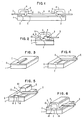
- FIGS. 1 and 2 there is shown a schematic cross sectional view of the external connection immobilization and environmental protection encapsulation of the invention as applied in FIG. 1 to a beam lead type structure and in FIG. 2 to a wire bond type structure.
- an integrated circuit chip 1 is provided with example contact pads 2 at opposite edges to which beam leads 3 are bonded.
- the bond between the beam lead 3 and the pad 2 is subject to vibrational stresses and shear stress due to different expansion performance of the parts in the package assembly.
- a connecting element 4 of wire is bonded both to the pad 2 and to an external conductor 5.
- the "wire bond" type structure 4 is subject to vibrational stresses and side "wire sweep" stresses that occur in injection molding.
- the chip 1 generally will have a passivated surface shown schematically as a single layer 6 through which the connecting pads 2 extend.
- the passivation protects the circuitry of the integrated circuit from environmental effects.
- the pads 2 are generally of a good conductor material such as copper, aluminum or solder, and frequently extend above the surface of the passivation 6 as bumps.
- the beam leads 3 or wires 4 are fused to the pads 2 at bonds 8.
- the effect of stress at the bond 8 is prevented by providing localized immobilizing material 9 at the location of the bonds 8 and in an area 10 of contact with the chip surface that is restricted to the vicinity of the pad 2 and extending vertically high enough to surround and cover the beam lead bond 8 or wire bonds 8 where contact is made to the pad 2.
- the immobilizing material 9 has a high Young's modulus thereby imparting reinforcement and immobilization, and, since the area of contact 10 is restricted to only the vicinity of the pads 2, the material 9 should have a low temperature coefficient of expansion (TCE) property.
- TCE temperature coefficient of expansion
- materials usable as the material 9, such as the "filled" epoxy plastic materials that have a high Young's modulus have a substantial mismatch with the temperature/expansion performance of semiconductors and hence produce stresses when used over a broad semiconductor surface 15, such as the area between the pads 2 in FIG. 1 or beyond the material 9 in FIG. 2.
- an environmental protection material 11 is provided over the entire surface including the localized immobilizing material 9.
- the material 11 protects from such environmental effects as water vapor and physical contact with objects such as could occur during shelf life.
- the material 11 has a low Young's modulus. In applications, such as one where an hermetically sealed container is employed, the function of the environmental protection material 11 would be performed in a different way by the container.
- Young's modulus which is also known as the modulus of elasticity is a constant that expresses the ratio of unit stress to unit deformation for all values to the proportional limit of the material. The greater the Young's modulus the less deformation will occur for any unit stress.
- Young's modulus Some materials including plastics which are brittle or are very hard, have their performance constants in terms of fiber stresses or flexural strength. This modulus is related to Young's modulus and is known as the flexural modulus. These moduli are well tabulated in the handbooks used in the art. For purposes of clarity in explanation, all performance moduli will be referred to as Young's modulus.
- TCE temperature coefficient of expansion
- the TCE of Silicon semiconductor material is 2.3 (parts per million per degree C)
- the TCE of filled Epoxy plastic is about 20
- the TCE of Silicone is about 200.
- the Young's modulus of Silicone is very low.
- FIGS. 3 to 6 the beam lead interconnection technology of the invention is shown in greater detail using the same reference numerals.
- the width of the beam leads and the spacing between them is approaching 1 micrometer in the art.
- a schematic illustration of the pad on the chip is provided.
- a pad 2 extends from the circuitry in the chip, not shown. Since the pad 2 serves as an electrical connection, it has the properties of high electrical conductivity and bondability with the beam leads to be used.
- a bump either on the pad or the beam lead is used for registration and to provide bonding material.
- the pad 2 is shown extending above the surface 6 as a bump.
- connection 8 is schematically shown as having fillets.
- the beam lead 3 to pad 2 connection 8 is immobilized by providing on a localized region surrounding the pad 2 and beam lead 3 a quantity of a material 9 that has a high Young's modulus.
- the material 9 is shown cutaway at 12 and 13 to show the location of the connection 8 within it.
- the material 9 extends for a distance 14 on each side of the pad 2 about the width of the beam lead 3, extending under and above the beam lead 3, but ending before the edge of the chip and not extending over the broad surface area of the chip. Under those conditions, the connection is fully immobilized yet residual stresses on the chip surface are avoided. Where the pads are in line at the edge of the chip, the material 9 can be an annulus.
- FIG. 6 a schematic three-dimensional view of the invention is shown with the environmental protecting material 11 extending from the chip edge over the immobilizing material 9 and then continuing over the broad chip face illustrated as region 15.
- the environmental protecting material has a high TCE, compatible with the chip and further has a low Young's modulus. These conditions permit the avoidance of residual stresses at the passivation 6 material 11 interface and failures due to chip cracking and loss of adhesion.
- FIG. 7 The invention is illustrated in FIG. 7 in a three-dimensional schematic cutaway view in the TAB type technology, again using the same reference numerals.
- the chip 1 is positioned in an aperture 16 in a tape 17 that supports the beam leads 3, the external circuit connection ends of which are positioned on non-conducting supports 18.
- the tape 17 is advanced using sprocket-like mating openings 19.
- the pads 2 are shown in a line at the vicinity of the chip edge and the immobilizing material 9 is in the form of an annulus. It will be apparent that in chips having pad configurations that are positioned further in from the edge of the chip, discrete areas or multiple annuluses can be provided.
- the immobilizing material may be any non-conducting material having a high Young's modulus. It should be sufficiently pliable in application to be able to go under the lead 3 next to the pad 2 as illustrated in FIG. 5. There are members of the class of plastic materials known as epoxy resins that provide satisfactory Young's modulus values.
- the immobilizing material 9 is applied after the bonding of the leads 3 to the pads 2 coating an area 10 around the pad 2 to a narrow dimension on the surface illustrated as 14 or where the pads 2 are in a line at the edge as an annulus but not extending as far as the chip edge or over the broad chip surface. Where the material 9 is applied in an uncured state, the curing next takes place. The resulting structure immobilizes the bond 8 from stresses in all directions.
- Equation 2 the shear stress ⁇ exerted by this force, that in the absence of this invention would have been concentrated on bond 8, will be as shown in Equation 2.
- a TOT is the total effective area, which in turn is the sum of the areas of the pad 3, assigned the symbol A PAD and the area of contact of the material 9 with the surface of the passivation 6, assigned the symbol A ENC .
- Equation 4 K EFF is the effective shear modulus and is as set forth in Equation 5.
- K PAD and K ENC are the shear moduli of the pad 2 and material 9, respectively, and are constants of the particular materials employed.
- Equation 6 which describes the effective shear strain.
- K ENC A ENC due to the material 9 describes the immobilization effect of the material 9 and decreases shear strain on the bond 8 because of this effect. Since the total shear force F EXP is a fixed relationship for a given chip, lead, support combination such immobilization reduces the effective deformation as processing and service cycles occur thereby enhancing fatigue life.
- the entire chip face, including over the localized area immobilizing material 9 is covered with a low Young's modulus, high TCE material 11 that provides environmental protection such as from moisture and some mechanical protection from particles and handling. Where an hermetic package is employed and no handling damage is anticipated, the material 11 could be omitted. However, the material 11 is conveniently applied shortly after the material 9 is cured and at that time frequently not all potential handling hazards or environmental considerations are fully envisioned so that the material 11 is also effective in damage prevention.
- the silicone type materials have the requisite characteristics to serve as the material 11.
- the chip 1 would be one of silicon (Si) with a passivation 6 of an oxide of silicon (SiO x ) or gallium arsenide (GaAs) with a passivation of silicon nitride (Si3N4).
- the pads 2 would have an area of about 4 micrometers with a pad to pad spacing of about 2 micrometers, they would be of lead-tin (PbSn) solder with a lead-tin (PbSn) solder coating on the end to be bonded of the beam lead 5 which is about 2 micrometer wide copper (Cu) thereby permitting a fused bond 8 at a temperature less than 300°C.
- the immobilizing material 9 is of filled epoxy such as that available in the art under the name Dexter-Hysol 4322 having a flexural modulus of 238,000 psi and a TCE of 30 parts per million per degree C.
- the environmental material 11 is of silicone such as that available in the art under the name Amicon 3622 having a flexural modulus of 61 psi and a TCE of 470 parts per million per degree C.
Landscapes
- Structures Or Materials For Encapsulating Or Coating Semiconductor Devices Or Solid State Devices (AREA)
- Wire Bonding (AREA)
Applications Claiming Priority (2)
| Application Number | Priority Date | Filing Date | Title |
|---|---|---|---|
| US36874089A | 1989-06-20 | 1989-06-20 | |
| US368740 | 1999-08-05 |
Publications (2)
| Publication Number | Publication Date |
|---|---|
| EP0403783A2 true EP0403783A2 (de) | 1990-12-27 |
| EP0403783A3 EP0403783A3 (de) | 1991-07-17 |
Family
ID=23452539
Family Applications (1)
| Application Number | Title | Priority Date | Filing Date |
|---|---|---|---|
| EP19900109006 Withdrawn EP0403783A3 (de) | 1989-06-20 | 1990-05-12 | Einkapselung hoher Festigkeit und niedriger Spannung für Halbleitervorrichtungen |
Country Status (2)
| Country | Link |
|---|---|
| EP (1) | EP0403783A3 (de) |
| JP (1) | JPH0758747B2 (de) |
Families Citing this family (1)
| Publication number | Priority date | Publication date | Assignee | Title |
|---|---|---|---|---|
| US6239489B1 (en) * | 1999-07-30 | 2001-05-29 | Micron Technology, Inc. | Reinforcement of lead bonding in microelectronics packages |
Family Cites Families (1)
| Publication number | Priority date | Publication date | Assignee | Title |
|---|---|---|---|---|
| JPH01238150A (ja) * | 1988-03-18 | 1989-09-22 | Fujitsu Ltd | 半導体装置 |
-
1990
- 1990-05-12 EP EP19900109006 patent/EP0403783A3/de not_active Withdrawn
- 1990-06-20 JP JP2160064A patent/JPH0758747B2/ja not_active Expired - Lifetime
Also Published As
| Publication number | Publication date |
|---|---|
| JPH0334447A (ja) | 1991-02-14 |
| JPH0758747B2 (ja) | 1995-06-21 |
| EP0403783A3 (de) | 1991-07-17 |
Similar Documents
| Publication | Publication Date | Title |
|---|---|---|
| US5136366A (en) | Overmolded semiconductor package with anchoring means | |
| US6709895B1 (en) | Packaged microelectronic elements with enhanced thermal conduction | |
| US5172213A (en) | Molded circuit package having heat dissipating post | |
| EP0660383B1 (de) | Gehäuse für elektronische Bauelemente | |
| US5106784A (en) | Method of making a post molded cavity package with internal dam bar for integrated circuit | |
| US6020219A (en) | Method of packaging fragile devices with a gel medium confined by a rim member | |
| EP0778617A2 (de) | Elektronische Packungsanordnung umhüllt von einem geschmeidigen Medium, lateral begrenzt durch einen Kunststoffrand | |
| US6927095B2 (en) | Low cost and compliant microelectronic packages for high I/O and fine pitch | |
| US5834835A (en) | Semiconductor device having an improved structure for storing a semiconductor chip | |
| KR20020079477A (ko) | 다중소자모듈 형태의 반도체 장치 | |
| US8487428B2 (en) | Method and system for providing a reliable semiconductor assembly | |
| US5053852A (en) | Molded hybrid IC package and lead frame therefore | |
| EP0520679A2 (de) | Verfahren zur Herstellung eines vorgeformten Verpackungssystems | |
| US6312972B1 (en) | Pre-bond encapsulation of area array terminated chip and wafer scale packages | |
| US5047834A (en) | High strength low stress encapsulation of interconnected semiconductor devices | |
| KR970007840B1 (ko) | 반도체 장치 | |
| US12119280B2 (en) | Semiconductor device package with reduced stress | |
| US3793474A (en) | Lead configurations for plastic encapsulated semiconductor devices | |
| EP0430204B1 (de) | Kunststoffumhüllte Halbleiteranordnung | |
| EP0403783A2 (de) | Einkapselung hoher Festigkeit und niedriger Spannung für Halbleitervorrichtungen | |
| US6265768B1 (en) | Chip scale package | |
| EP0778616A2 (de) | Verfahren zum Verpacken von Anordnungen mit einem Gel, begrenzt durch ein Randelement | |
| JP2982971B2 (ja) | インターナル・ダム・バーを有する集積回路用ポスト・モールド・キャビティ型パッケージ | |
| US6429517B1 (en) | Semiconductor device and fabrication method thereof | |
| KR100454774B1 (ko) | 반도체장치 |
Legal Events
| Date | Code | Title | Description |
|---|---|---|---|
| PUAI | Public reference made under article 153(3) epc to a published international application that has entered the european phase |
Free format text: ORIGINAL CODE: 0009012 |
|
| AK | Designated contracting states |
Kind code of ref document: A2 Designated state(s): DE FR GB |
|
| 17P | Request for examination filed |
Effective date: 19901213 |
|
| PUAL | Search report despatched |
Free format text: ORIGINAL CODE: 0009013 |
|
| AK | Designated contracting states |
Kind code of ref document: A3 Designated state(s): DE FR GB |
|
| 17Q | First examination report despatched |
Effective date: 19930630 |
|
| STAA | Information on the status of an ep patent application or granted ep patent |
Free format text: STATUS: THE APPLICATION IS DEEMED TO BE WITHDRAWN |
|
| 18D | Application deemed to be withdrawn |
Effective date: 19940618 |