EP0400643A2 - Amplifying apparatus with a differential amplifier stage - Google Patents
Amplifying apparatus with a differential amplifier stage Download PDFInfo
- Publication number
- EP0400643A2 EP0400643A2 EP90110362A EP90110362A EP0400643A2 EP 0400643 A2 EP0400643 A2 EP 0400643A2 EP 90110362 A EP90110362 A EP 90110362A EP 90110362 A EP90110362 A EP 90110362A EP 0400643 A2 EP0400643 A2 EP 0400643A2
- Authority
- EP
- European Patent Office
- Prior art keywords
- transistor
- base
- signal
- differential amplifier
- amplifier stage
- Prior art date
- Legal status (The legal status is an assumption and is not a legal conclusion. Google has not performed a legal analysis and makes no representation as to the accuracy of the status listed.)
- Granted
Links
- 230000005236 sound signal Effects 0.000 claims description 5
- 230000002401 inhibitory effect Effects 0.000 claims description 4
- 238000001514 detection method Methods 0.000 claims description 2
- 230000005764 inhibitory process Effects 0.000 claims 1
- 230000035939 shock Effects 0.000 description 19
- 239000003990 capacitor Substances 0.000 description 15
- 230000007423 decrease Effects 0.000 description 4
- 230000008878 coupling Effects 0.000 description 3
- 238000010168 coupling process Methods 0.000 description 3
- 238000005859 coupling reaction Methods 0.000 description 3
- 238000010586 diagram Methods 0.000 description 3
- 230000002411 adverse Effects 0.000 description 1
- 230000000694 effects Effects 0.000 description 1
- 239000007858 starting material Substances 0.000 description 1
Images
Classifications
-
- H—ELECTRICITY
- H03—ELECTRONIC CIRCUITRY
- H03F—AMPLIFIERS
- H03F3/00—Amplifiers with only discharge tubes or only semiconductor devices as amplifying elements
- H03F3/34—DC amplifiers in which all stages are DC-coupled
- H03F3/343—DC amplifiers in which all stages are DC-coupled with semiconductor devices only
-
- H—ELECTRICITY
- H03—ELECTRONIC CIRCUITRY
- H03F—AMPLIFIERS
- H03F1/00—Details of amplifiers with only discharge tubes, only semiconductor devices or only unspecified devices as amplifying elements
- H03F1/30—Modifications of amplifiers to reduce influence of variations of temperature or supply voltage or other physical parameters
- H03F1/305—Modifications of amplifiers to reduce influence of variations of temperature or supply voltage or other physical parameters in case of switching on or off of a power supply
Definitions
- the present invention generally relates to an amplifying apparatus with a differential amplifier stage located at the input stage. More particularly, this invention is directed to an amplifying apparatus suitable for a low frequency signal, which reduces shock noise that occurs when a power supply is switched on or off.
- an amplifying apparatus for amplifying a sound signal should meet severe requirements against shock noise that is generated in accordance with the ON/OFF action of the power supply.
- a power amplifying apparatus for driving loudspeakers according to an output signal from the mentioned amplifier apparatus there is a demand for an ability to suppress undesirable shock noise which is generated from loudspeakers when the power supply is switched on or off.
- this means uses a decoupling capacitor or ripple filter capacitor connected to a power circuit, and utilizes a time constant set by a circuit including such a capacitor to mute a sound signal output.
- Fig. 3 exemplifies a conventional amplifying apparatus which suppresses shock noise caused according to the ON/OFF action of a power supply.
- a capacitor 11 and resistors 12, 13 and 14 constitute a ripple filter circuit.
- a power supply voltage V CC is divided by the resistors 12 and 13, connected in series, and the divided voltage is supplied via the resistor 14 to the capacitor 11.
- the voltage V CC is further divided by resistors 15 and 16, and the divided voltage is supplied to the bases of transistors 17 and 18 whose emitters are supplied via the resistors 12 and 14 with the voltage V CC .
- the ratio of the resistances of the resistors 15 and 16 is so set that the base potential of the transistors 17 and 18 is equal to or higher than their emitter potential. That is, the transistors 17 and 18 are set off in the normal operational state.
- the transistor 17 thus controlled has its collector connected to the base of a transistor 19, which is connected in parallel to the capacitor 11, so that the transistor 17 when on sets the transistor 19 on to thereby discharge the capacitor 11.
- a signal from the collector of the transistor 18 is supplied to the base of the transistor 20, so that an output signal is output in the normal state where the former transistor 18 is rendered on.
- the transistor 17 is rendered off, so is the transistor 19, thus permitting the capacitor 11 to be charged by the voltage V CC via the resistors 12 and 14.
- the transistor 20 is rendered off and an output signal is properly output.
- an object of the present invention to provide an amplifying apparatus with a differential amplifier stage, which can effectively suppress generation of shock noise originating from an ON/OFF control of a power supply, particularly originating from the OFF operation of the power supply, so as to prevent the adverse influence of the shock noise from appearing on the output.
- the amplifying apparatus with a differential amplifier stage comprises power-off detecting means for detecting the stop of an amplifying operation caused by switching a power supply off, first input control means for inhibiting an input to a differential amplifier circuit in accordance with power-off detection by the power-off detecting means, differential input detecting means for detecting an input to the differential amplifier circuit, and second input control means for inhibiting an input to a negative feedback side of the differential amplifier circuit when the differential input detecting means detects a reduction in the input.
- the power-off detecting means detects the power-off of the power supply and the first input control means inhibits an input to the differential amplifier stage.
- the differential input detecting means detects the falling of the input signal and causes the second input control means to inhibit a negative feedback input to the differential input stage.
- the power supply is switched off, therefore, the input signal as well as the negative feedback input are inhibited from being input to the differential input stage.
- the unbalanced state of the differential amplifier stage is therefore corrected quickly with the power-off action of the power supply, thus effective suppressing shock noise originating from an amplified output even when the power supply is sequentially subjected to an ON/OFF control.
- Fig. 1 presents a low frequency amplifying apparatus with a differential amplifier stage 30, which amplifies a sound signal.
- the differential amplifier stage 30, which comprises a pair of PNP transistors 31 and 32, performs a differential operation.
- the transistors 31 and 32 have their emitters supplied with a power supply voltage V CC through a constant current circuit 33, and their collectors connected to the collectors of NPN transistors 34 and 35 which constitute a current mirror circuit.
- the transistors 34 and 35 have their emitters grounded through resistors 36 and 37, and their bases connected together to the collector of the transistor 35.
- An output signal from the collector of the transistor 34 is amplified by an amplifier 38 as needed, and supplied to an output terminal 39.
- This amplifying apparatus has the same circuit as the one shown in Fig. 3 for suppressing shock noises; the same reference numerals as given in Fig. 3 are used to specify the corresponding or identical elements.
- a capacitor 11, which is connected in parallel to a transistor 19, is always charged by the voltage V CC via resistors 12 and 14.
- the voltage V CC is divided by resistors 15 and 16, and transistors 17 and 18 are controlled with the divided voltage.
- the emitters of the transistors 17 and 18 are connected, together with the collector of a transistor 19, to a bias circuit (not shown).
- the transistors 17 and 18 are rendered on.
- the transistor 17 turns on the transistor 19 to discharge the capacitor 11, while the transistor 18 turns on a transistor 20, thus preventing shock noise from being output when the voltage V CC is turned off.
- the node between the resistors 15 and 16 is connected to the base of a PNP transistor 40.
- This transistor 40 has its emitter connected via the resistors 12 and 14 to the voltage V CC , and its collector connected to the base of an NPN transistor 41.
- the transistor 40 When the voltage V CC is in the normal state, the transistor 40 is rendered off together with the transistors 17 and 18.
- the transistor 40 is rendered on. In other words, this transistor 40 constitutes means of detecting the of the power supply voltage.
- the transistor 41 is turned on accordingly.
- the transistor 41 is connected between the ground and the base of the transistor 31 on the input side, one element of the differential amplifier stage 30.
- the transistor 41 When the transistor 41 is turned on, the input signal is grounded, and the level of an input signal to the differential amplifier stage 30 is reduced to the ground level. That is, the transistor 41 constitutes the first input control means for the differential amplifier stage 30.
- the input signal of the transistor 31 is further sent to the base of a PNP transistor 42.
- the transistor 42 has its emitter supplied with a signal that is supplied to the base of the transistor 32, and its collector connected to the base of a transistor 43.
- the transistor 42 is turned on, and it constitutes differential input detecting means which is controlled according to the status of the differential input.
- the transistor 43 is rendered on.
- the transistor 32 another element of the differential amplifier stage 30, has its base supplied with a signal for negative feedback (NF) from the output terminal 39 as a negative feedback signal through a feedback resistor 44.
- the transistor 43 has its collector connected to the base of the transistor 32, and its emitter grounded. In other words, the transistor 43 when on causes the base of the transistor 32 to have a ground potential, and constitutes the second input control means on the NF side.
- the base of the transistor 32 is further grounded via a feedback resistor 45 and an NF coupling capacitor 46.
- the transistor 19 is turned on by the transistor 17 so as to discharge the capacitor 11, and the transistor 20 is turned on by the transistor 18 so as to mute the output.
- the transistor 40 is turned on together with the transistors 17 and 18, so that the transistor 41 is turned on to thereby drastically decrease the level of an input signal IN of the input differential amplifier stage 30.
- the potential does not sharply decrease because of the presence of a coupling capacitor 46.
- the transistor 42 is turned on to render the transistor 43 on.
- the transistor 43 coupling capacitor 46 is then rapidly discharged by the transistor 43, which rapidly decreases the levels of the signals on both the input signal and the NF input side of the input differential amplifier stage 30.
- the unbalanced state after the power supply is switched off is quickly relieved. Even if the power supply is sequentially turned on and off, the differential amplifier stage 30 can surely prevent the shock noise originating from the power-off operation from being output.
- Fig. 2 illustrates the second embodiment of the amplifying apparatus as applied to a stand-by circuit.
- Transistors 52 and 53 are controlled by a command signal from a stand-by command terminal 51, and a switching transistor 54 is controlled by the transistor 52.
- the transistors 52 to 54 constitute a stand-by switching circuit; the transistors 52 and 53 are controlled on the basis of a stand-by command signal supplied to the stand-by command terminal 51, with the switching transistor 54 serving to control the supply and cutoff of the power supply voltage V CC supplied to a stand-by line 55.
- the transistor 53 is connected to a ripple filter line 57 through a resistor 56.
- the stand-by circuit is used to reduce power consumption which increases when the voltage V CC is kept supplied.
- This stand-by circuit controls the transistor 54 based on the command signal input to the stand-by command terminal 51, and cuts off the power from the power supply of the amplifying apparatus as needed to render the amplifying apparatus inoperative.
- the base of the transistor 41 is supplied with a signal from the collector of the transistor 53.
- the transistor 53 which has cut off the base current of the transistor 41 when the amplifying apparatus is operated, turns on the transistor 41 in the stand-by state and lowers the level of the input signal IN of the transistor 31 in the differential amplifier stage 30. Thereafter, the transistors 42 and 43 are controlled in the same manner as done in the embodiment shown in Fig. 1, and the unbalanced state of the differential amplifier stage 30 is quickly relieved.
- the present invention can apply other circuits than those of the aforementioned embodiments.
- the foregoing description of the embodiments has been given with a reference to the amplifier circuit which deals with a low-frequency signal, such as a sound signal, the present invention can also apply to a high frequency amplifier circuit.
Landscapes
- Engineering & Computer Science (AREA)
- Power Engineering (AREA)
- Amplifiers (AREA)
Abstract
Description
- The present invention generally relates to an amplifying apparatus with a differential amplifier stage located at the input stage. More particularly, this invention is directed to an amplifying apparatus suitable for a low frequency signal, which reduces shock noise that occurs when a power supply is switched on or off.
- For instance, an amplifying apparatus for amplifying a sound signal should meet severe requirements against shock noise that is generated in accordance with the ON/OFF action of the power supply. Particularly, regarding a power amplifying apparatus for driving loudspeakers according to an output signal from the mentioned amplifier apparatus, there is a demand for an ability to suppress undesirable shock noise which is generated from loudspeakers when the power supply is switched on or off.
- There is known means for suppressing such shock noise; this means uses a decoupling capacitor or ripple filter capacitor connected to a power circuit, and utilizes a time constant set by a circuit including such a capacitor to mute a sound signal output.
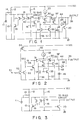
- Fig. 3 exemplifies a conventional amplifying apparatus which suppresses shock noise caused according to the ON/OFF action of a power supply. A
capacitor 11 andresistors resistors resistor 14 to thecapacitor 11. - The voltage VCC is further divided by
resistors transistors resistors resistors transistors transistors - The
transistor 17 thus controlled has its collector connected to the base of atransistor 19, which is connected in parallel to thecapacitor 11, so that thetransistor 17 when on sets thetransistor 19 on to thereby discharge thecapacitor 11. A signal from the collector of thetransistor 18 is supplied to the base of thetransistor 20, so that an output signal is output in the normal state where theformer transistor 18 is rendered on. - In other words, in the normal operational state where the power supply voltage VCC is set, the
transistor 17 is rendered off, so is thetransistor 19, thus permitting thecapacitor 11 to be charged by the voltage VCC via theresistors transistor 18 is off, thetransistor 20 is rendered off and an output signal is properly output. - When the power supply is switched off in such a state, the voltage VCC falls and the base potential of the
transistors transistors transistors transistor 19 being on permits thecapacitor 11 to be discharged. At the same time, the output signal is led to the ground by thetransistor 20 to cut off the output, thereby preventing shock noise from being generated by the power off of the power supply. - The use of the above-described circuit is effective in suppressing shock noise which is generated in accordance with the OFF operation of a single power supply, but cannot cope with a case where the ON/OFF operation of the power supply is sequentially repeated. When such an amplifier circuit is constituted by an integrated circuit, a differential amplifier circuit is provided at the input stage though not shown in Fig. 3. Such a differential amplifier circuit often has different time constants on one input side which is supplied with an input signal and the other input side which is supplied with an output signal as a negative feedback signal, and this circuit is in an unbalanced state. When the power supply is switched off, switched on again, then switched off again, therefore, the unbalanced state of this differential circuit would directly appear as a variation in the output and would be output as shock noise.
- For instance, in an amplifier circuit provided in a stereo system for an automobile, when a starter motor is operated to start the engine through operation of an ignition key, the power for the stereo system is cut off for a very short period of time, in which case, particularly, the generation of the aforementioned shock noise should be considered.
- Accordingly, it is an object of the present invention to provide an amplifying apparatus with a differential amplifier stage, which can effectively suppress generation of shock noise originating from an ON/OFF control of a power supply, particularly originating from the OFF operation of the power supply, so as to prevent the adverse influence of the shock noise from appearing on the output.
- It is another object of this invention to provide an amplifying apparatus which can effectively prevent generation of shock noise originating particularly from the power-off operation following the second one in a case where the ON/OFF operation of the power supply is repeated.
- It is a further object of this invention to provide an amplifying apparatus with a differential amplifier stage, which can surely suppress unpleasant shock noise to provide good sound outputs, when applied even to an audio apparatus that is installed in an automobile and has its power supply frequently switched on and off.
- The amplifying apparatus with a differential amplifier stage according to this invention comprises power-off detecting means for detecting the stop of an amplifying operation caused by switching a power supply off, first input control means for inhibiting an input to a differential amplifier circuit in accordance with power-off detection by the power-off detecting means, differential input detecting means for detecting an input to the differential amplifier circuit, and second input control means for inhibiting an input to a negative feedback side of the differential amplifier circuit when the differential input detecting means detects a reduction in the input.
- In the thus constituted amplifying apparatus having the differential amplifier stage, the power-off detecting means detects the power-off of the power supply and the first input control means inhibits an input to the differential amplifier stage. At the same time, the differential input detecting means detects the falling of the input signal and causes the second input control means to inhibit a negative feedback input to the differential input stage. When the power supply is switched off, therefore, the input signal as well as the negative feedback input are inhibited from being input to the differential input stage. The unbalanced state of the differential amplifier stage is therefore corrected quickly with the power-off action of the power supply, thus effective suppressing shock noise originating from an amplified output even when the power supply is sequentially subjected to an ON/OFF control.
- This invention can be more fully understood from the following detailed description when taken in conjunction with the accompanying drawings, in which:
- Fig. 1 is a circuit diagram for explaining the first embodiment of an amplifying apparatus of the present invention;
- Fig. 2 is a circuit diagram exemplifying the second embodiment of the present invention as applied to a stand-by circuit; and
- Fig. 3 is a circuit diagram exemplifying a shock noise preventing circuit applied to a conventional amplifying apparatus in order to avoid shock noises.
- Preferred embodiments of this invention will now be described referring to the accompanying drawings.
- Fig. 1 presents a low frequency amplifying apparatus with a differential amplifier stage 30, which amplifies a sound signal. The differential amplifier stage 30, which comprises a pair of
PNP transistors 31 and 32, performs a differential operation. Thetransistors 31 and 32 have their emitters supplied with a power supply voltage VCC through a constantcurrent circuit 33, and their collectors connected to the collectors ofNPN transistors transistors resistors transistor 35. An output signal from the collector of thetransistor 34 is amplified by anamplifier 38 as needed, and supplied to anoutput terminal 39. - This amplifying apparatus has the same circuit as the one shown in Fig. 3 for suppressing shock noises; the same reference numerals as given in Fig. 3 are used to specify the corresponding or identical elements. A
capacitor 11, which is connected in parallel to atransistor 19, is always charged by the voltage VCC viaresistors resistors transistors transistors transistor 19, to a bias circuit (not shown). When the power supply voltage falls, thetransistors transistor 17 turns on thetransistor 19 to discharge thecapacitor 11, while thetransistor 18 turns on atransistor 20, thus preventing shock noise from being output when the voltage VCC is turned off. - The node between the
resistors PNP transistor 40. Thistransistor 40 has its emitter connected via theresistors NPN transistor 41. When the voltage VCC is in the normal state, thetransistor 40 is rendered off together with thetransistors transistor 40 is rendered on. In other words, thistransistor 40 constitutes means of detecting the of the power supply voltage. When thetransistor 40 is turned on, thetransistor 41 is turned on accordingly. - The
transistor 41 is connected between the ground and the base of thetransistor 31 on the input side, one element of the differential amplifier stage 30. When thetransistor 41 is turned on, the input signal is grounded, and the level of an input signal to the differential amplifier stage 30 is reduced to the ground level. That is, thetransistor 41 constitutes the first input control means for the differential amplifier stage 30. - The input signal of the
transistor 31 is further sent to the base of aPNP transistor 42. Thetransistor 42 has its emitter supplied with a signal that is supplied to the base of the transistor 32, and its collector connected to the base of atransistor 43. In other words, when the level of the input signal to the differential amplifier stage 30 decreases, thetransistor 42 is turned on, and it constitutes differential input detecting means which is controlled according to the status of the differential input. When thetransistor 42 is turned on, thetransistor 43 is rendered on. - The transistor 32, another element of the differential amplifier stage 30, has its base supplied with a signal for negative feedback (NF) from the
output terminal 39 as a negative feedback signal through afeedback resistor 44. Thetransistor 43 has its collector connected to the base of the transistor 32, and its emitter grounded. In other words, thetransistor 43 when on causes the base of the transistor 32 to have a ground potential, and constitutes the second input control means on the NF side. The base of the transistor 32 is further grounded via afeedback resistor 45 and anNF coupling capacitor 46. - When the voltage VCC is turned off in the thus constituted circuit, the
transistor 19 is turned on by thetransistor 17 so as to discharge thecapacitor 11, and thetransistor 20 is turned on by thetransistor 18 so as to mute the output. - Further, the
transistor 40 is turned on together with thetransistors transistor 41 is turned on to thereby drastically decrease the level of an input signal IN of the input differential amplifier stage 30. - On the NF side of the differential amplifier stage 30, however, the potential does not sharply decrease because of the presence of a
coupling capacitor 46. However, if the potential on the side of the input IN of the differential amplifier stage 30 drastically drops by thetransistor 41, thetransistor 42 is turned on to render thetransistor 43 on. Thetransistor 43coupling capacitor 46 is then rapidly discharged by thetransistor 43, which rapidly decreases the levels of the signals on both the input signal and the NF input side of the input differential amplifier stage 30. Therefore, the unbalanced state after the power supply is switched off is quickly relieved. Even if the power supply is sequentially turned on and off, the differential amplifier stage 30 can surely prevent the shock noise originating from the power-off operation from being output. - Fig. 2 illustrates the second embodiment of the amplifying apparatus as applied to a stand-by circuit.
Transistors by command terminal 51, and a switchingtransistor 54 is controlled by thetransistor 52. In other words, thetransistors 52 to 54 constitute a stand-by switching circuit; thetransistors by command terminal 51, with the switchingtransistor 54 serving to control the supply and cutoff of the power supply voltage VCC supplied to a stand-by line 55. Thetransistor 53 is connected to aripple filter line 57 through aresistor 56. - The stand-by circuit is used to reduce power consumption which increases when the voltage VCC is kept supplied. This stand-by circuit controls the
transistor 54 based on the command signal input to the stand-by command terminal 51, and cuts off the power from the power supply of the amplifying apparatus as needed to render the amplifying apparatus inoperative. - The differential amplifier stage 30, which constitutes the input section of the amplifying apparatus, is supplied with the power over the stand-
by line 55. Since this section is the same as that of the first embodiment shown in Fig. 1, the same reference numerals as shown in Fig. 1 are used to specify the corresponding or identical elements in Fig. 2 and their otherwise redundant description will be omitted. The base of thetransistor 41 is supplied with a signal from the collector of thetransistor 53. - In the apparatus with such a structure, if the potential of the input signal to the stand-
by command terminal 51 falls down to or below a voltage VF in the forward PN direction of thetransistors transistors transistor 53, which has cut off the base current of thetransistor 41 when the amplifying apparatus is operated, turns on thetransistor 41 in the stand-by state and lowers the level of the input signal IN of thetransistor 31 in the differential amplifier stage 30. Thereafter, thetransistors - The present invention can apply other circuits than those of the aforementioned embodiments. For instance, although the foregoing description of the embodiments has been given with a reference to the amplifier circuit which deals with a low-frequency signal, such as a sound signal, the present invention can also apply to a high frequency amplifier circuit.
- Reference signs are added to the claims for reference purposes only and do not effect the scope".
Claims (9)
first input control means (41) for inhibiting an input to said differential amplifier stage (30) when a power-off state is detected by said power-off detecting means (40);
input detecting means (42), controlled based on an input signal to said differential amplifier stage (30), for detecting inhibition of said input signal; and
second input control means (43) for inhibiting said negative feedback signal to said differential amplifier stage (30) when said input detecting means (42) detects said input signal being inhibited.
a fourth transistor (41) of an NPN type, which is turned on based on a disabled-state detection signal from said third transistor (40), said fourth transistor (41) having a collector connected to said base of said first transistor (31) of said differential amplifier stage (30) and an emitter grounded;
a fifth transistor (42) of a PNP type having a base connected to said base of said first transistor (31) and an emitter connected to said base of said second transistor (32) of said differential amplifier stage (30); and
a sixth transistor (43) of an NPN type having a base connected to a collector of said fifth transistor (42), a collector connected to said base of said second transistor (32) and an emitter grounded.
Applications Claiming Priority (2)
| Application Number | Priority Date | Filing Date | Title |
|---|---|---|---|
| JP1138921A JP2609723B2 (en) | 1989-05-31 | 1989-05-31 | Amplifier circuit |
| JP138921/89 | 1989-05-31 |
Publications (3)
| Publication Number | Publication Date |
|---|---|
| EP0400643A2 true EP0400643A2 (en) | 1990-12-05 |
| EP0400643A3 EP0400643A3 (en) | 1991-05-22 |
| EP0400643B1 EP0400643B1 (en) | 1994-01-12 |
Family
ID=15233249
Family Applications (1)
| Application Number | Title | Priority Date | Filing Date |
|---|---|---|---|
| EP90110362A Expired - Lifetime EP0400643B1 (en) | 1989-05-31 | 1990-05-31 | Amplifying apparatus with a differential amplifier stage |
Country Status (5)
| Country | Link |
|---|---|
| US (1) | US5059919A (en) |
| EP (1) | EP0400643B1 (en) |
| JP (1) | JP2609723B2 (en) |
| KR (1) | KR960009445B1 (en) |
| DE (1) | DE69005903T2 (en) |
Families Citing this family (12)
| Publication number | Priority date | Publication date | Assignee | Title |
|---|---|---|---|---|
| JP2503112B2 (en) * | 1991-02-20 | 1996-06-05 | 新日本製鐵株式会社 | Manufacturing method of good electromagnetic plate |
| JP2503111B2 (en) * | 1991-02-20 | 1996-06-05 | 新日本製鐵株式会社 | Manufacturing method of non-oriented electromagnetic thick plate with excellent magnetic properties |
| JP2503110B2 (en) * | 1991-02-20 | 1996-06-05 | 新日本製鐵株式会社 | Method for manufacturing non-oriented electromagnetic thick plate with excellent magnetic properties |
| JPH04265580A (en) * | 1991-02-20 | 1992-09-21 | Fujitsu Ltd | Magnetic disk device |
| JP2503125B2 (en) * | 1991-05-09 | 1996-06-05 | 新日本製鐵株式会社 | Manufacturing method of good electromagnetic plate |
| JP2503123B2 (en) * | 1991-05-09 | 1996-06-05 | 新日本製鐵株式会社 | Manufacturing method of non-oriented electromagnetic thick plate with excellent magnetic properties |
| JP2503124B2 (en) * | 1991-05-09 | 1996-06-05 | 新日本製鐵株式会社 | Manufacturing method of good electromagnetic thick plate |
| JP2503122B2 (en) * | 1991-05-09 | 1996-06-05 | 新日本製鐵株式会社 | Method for manufacturing non-oriented electromagnetic thick plate with excellent magnetic properties |
| JP3112522B2 (en) * | 1991-09-11 | 2000-11-27 | ローム株式会社 | Audio signal amplifier circuit |
| JP2564994B2 (en) * | 1991-10-14 | 1996-12-18 | 日本鋼管株式会社 | Soft magnetic steel material excellent in direct current magnetization characteristics and corrosion resistance and method for producing the same |
| EP0576770B1 (en) * | 1992-05-22 | 1999-12-22 | STMicroelectronics S.r.l. | Audio Amplifier turn-off control circuit |
| FR2762504B1 (en) | 1997-04-29 | 1999-09-10 | Cird Galderma | HAIR REMOVAL PROCESS |
Citations (4)
| Publication number | Priority date | Publication date | Assignee | Title |
|---|---|---|---|---|
| JPS5471966A (en) * | 1977-11-18 | 1979-06-08 | Toshiba Corp | Low frequency amplifier circuit |
| JPS54139363A (en) * | 1978-04-20 | 1979-10-29 | Hitachi Ltd | Noise mute circuit |
| US4446441A (en) * | 1980-09-22 | 1984-05-01 | Olympus Optical Co., Ltd. | Transient noise free type amplifier circuit |
| EP0299665A2 (en) * | 1987-07-13 | 1989-01-18 | Kabushiki Kaisha Toshiba | Power amplifier circuit with a stand-by state |
-
1989
- 1989-05-31 JP JP1138921A patent/JP2609723B2/en not_active Expired - Fee Related
-
1990
- 1990-05-28 KR KR1019900007695A patent/KR960009445B1/en not_active IP Right Cessation
- 1990-05-30 US US07/530,619 patent/US5059919A/en not_active Expired - Lifetime
- 1990-05-31 DE DE69005903T patent/DE69005903T2/en not_active Expired - Fee Related
- 1990-05-31 EP EP90110362A patent/EP0400643B1/en not_active Expired - Lifetime
Patent Citations (4)
| Publication number | Priority date | Publication date | Assignee | Title |
|---|---|---|---|---|
| JPS5471966A (en) * | 1977-11-18 | 1979-06-08 | Toshiba Corp | Low frequency amplifier circuit |
| JPS54139363A (en) * | 1978-04-20 | 1979-10-29 | Hitachi Ltd | Noise mute circuit |
| US4446441A (en) * | 1980-09-22 | 1984-05-01 | Olympus Optical Co., Ltd. | Transient noise free type amplifier circuit |
| EP0299665A2 (en) * | 1987-07-13 | 1989-01-18 | Kabushiki Kaisha Toshiba | Power amplifier circuit with a stand-by state |
Non-Patent Citations (2)
| Title |
|---|
| PATENT ABSTRACTS OF JAPAN vol. 3, no. 159 (E-162)(31) 27 December 1979, & JP-A-54 139363 (HITACHI SEISAKUSHO K.K.) 29 October 1979, * |
| PATENT ABSTRACTS OF JAPAN vol. 3, no. 94 (E-129)(49) 10 August 1979, & JP-A-54 71966 (TOKYO SHIBAURA DENKI K.K.) 8 June 1979, * |
Also Published As
| Publication number | Publication date |
|---|---|
| DE69005903T2 (en) | 1994-06-16 |
| KR900019344A (en) | 1990-12-24 |
| KR960009445B1 (en) | 1996-07-19 |
| EP0400643A3 (en) | 1991-05-22 |
| JPH034606A (en) | 1991-01-10 |
| DE69005903D1 (en) | 1994-02-24 |
| US5059919A (en) | 1991-10-22 |
| JP2609723B2 (en) | 1997-05-14 |
| EP0400643B1 (en) | 1994-01-12 |
Similar Documents
| Publication | Publication Date | Title |
|---|---|---|
| KR100196258B1 (en) | Muting circuit for television | |
| EP0400643A2 (en) | Amplifying apparatus with a differential amplifier stage | |
| KR900007921B1 (en) | Sock noise prevention circuit of voice amp | |
| JP3315934B2 (en) | Series control type regulator | |
| EP0280327B1 (en) | Audio output amplifier | |
| JPH08213849A (en) | Audio mute circuit | |
| JPH0793537B2 (en) | Muting method | |
| US5317470A (en) | Control system including a switching circuit for ensuring proper operation when operating power is removed from a portion of the control system | |
| JP2869255B2 (en) | amplifier | |
| US6590446B2 (en) | Amplifier circuit and electronic apparatus using the same | |
| JPS6145622Y2 (en) | ||
| JP4483010B2 (en) | Power amplifier protection circuit | |
| JPH08148942A (en) | Amplifier | |
| JP2557628B2 (en) | Rituple Filter | |
| KR900010906Y1 (en) | Noice deduction circuit at power on-off | |
| JP2708982B2 (en) | Multipath noise detection circuit | |
| JPS6042644B2 (en) | power amplifier | |
| JP3332102B2 (en) | Shock noise prevention circuit | |
| JP2000244256A (en) | Protecting circuit | |
| KR20020069463A (en) | Popcorn noise rejection circuit of audio apparatus | |
| JPH0513047Y2 (en) | ||
| JPH11243323A (en) | Control circuit for amplifier circuit | |
| JP2008067187A (en) | Muting circuit and semiconductor integrated circuit equipped with the same | |
| JPH10160769A (en) | Overcurrent detection circuit | |
| JPS6113407B2 (en) |
Legal Events
| Date | Code | Title | Description |
|---|---|---|---|
| PUAI | Public reference made under article 153(3) epc to a published international application that has entered the european phase |
Free format text: ORIGINAL CODE: 0009012 |
|
| 17P | Request for examination filed |
Effective date: 19900531 |
|
| AK | Designated contracting states |
Kind code of ref document: A2 Designated state(s): DE FR GB NL |
|
| PUAL | Search report despatched |
Free format text: ORIGINAL CODE: 0009013 |
|
| AK | Designated contracting states |
Kind code of ref document: A3 Designated state(s): DE FR GB NL |
|
| 17Q | First examination report despatched |
Effective date: 19930217 |
|
| RAP1 | Party data changed (applicant data changed or rights of an application transferred) |
Owner name: TOSHIBA AUDIO VIDEO ENGINEERING CO., LTD. Owner name: KABUSHIKI KAISHA TOSHIBA |
|
| GRAA | (expected) grant |
Free format text: ORIGINAL CODE: 0009210 |
|
| AK | Designated contracting states |
Kind code of ref document: B1 Designated state(s): DE FR GB NL |
|
| REF | Corresponds to: |
Ref document number: 69005903 Country of ref document: DE Date of ref document: 19940224 |
|
| ET | Fr: translation filed | ||
| PLBE | No opposition filed within time limit |
Free format text: ORIGINAL CODE: 0009261 |
|
| STAA | Information on the status of an ep patent application or granted ep patent |
Free format text: STATUS: NO OPPOSITION FILED WITHIN TIME LIMIT |
|
| RAP2 | Party data changed (patent owner data changed or rights of a patent transferred) |
Owner name: TOSHIBA AVE CO., LTD Owner name: KABUSHIKI KAISHA TOSHIBA |
|
| 26N | No opposition filed | ||
| NLT2 | Nl: modifications (of names), taken from the european patent patent bulletin |
Owner name: KABUSHIKI KAISHA TOSHIBA TE KAWASAKI EN TOSHIBA AV |
|
| PGFP | Annual fee paid to national office [announced via postgrant information from national office to epo] |
Ref country code: FR Payment date: 19970513 Year of fee payment: 8 |
|
| PGFP | Annual fee paid to national office [announced via postgrant information from national office to epo] |
Ref country code: GB Payment date: 19970522 Year of fee payment: 8 |
|
| PGFP | Annual fee paid to national office [announced via postgrant information from national office to epo] |
Ref country code: DE Payment date: 19970606 Year of fee payment: 8 |
|
| PG25 | Lapsed in a contracting state [announced via postgrant information from national office to epo] |
Ref country code: GB Free format text: LAPSE BECAUSE OF NON-PAYMENT OF DUE FEES Effective date: 19980531 Ref country code: FR Free format text: LAPSE BECAUSE OF NON-PAYMENT OF DUE FEES Effective date: 19980531 |
|
| GBPC | Gb: european patent ceased through non-payment of renewal fee |
Effective date: 19980531 |
|
| PG25 | Lapsed in a contracting state [announced via postgrant information from national office to epo] |
Ref country code: DE Free format text: LAPSE BECAUSE OF NON-PAYMENT OF DUE FEES Effective date: 19990302 |
|
| REG | Reference to a national code |
Ref country code: FR Ref legal event code: ST |
|
| PGFP | Annual fee paid to national office [announced via postgrant information from national office to epo] |
Ref country code: NL Payment date: 20070503 Year of fee payment: 18 |
|
| PG25 | Lapsed in a contracting state [announced via postgrant information from national office to epo] |
Ref country code: NL Free format text: LAPSE BECAUSE OF NON-PAYMENT OF DUE FEES Effective date: 20081201 |