EP0397304B1 - Method and structure for wiring connection of a display device - Google Patents
Method and structure for wiring connection of a display device Download PDFInfo
- Publication number
- EP0397304B1 EP0397304B1 EP90302758A EP90302758A EP0397304B1 EP 0397304 B1 EP0397304 B1 EP 0397304B1 EP 90302758 A EP90302758 A EP 90302758A EP 90302758 A EP90302758 A EP 90302758A EP 0397304 B1 EP0397304 B1 EP 0397304B1
- Authority
- EP
- European Patent Office
- Prior art keywords
- electrodes
- substrate
- display
- display substrate
- display device
- Prior art date
- Legal status (The legal status is an assumption and is not a legal conclusion. Google has not performed a legal analysis and makes no representation as to the accuracy of the status listed.)
- Expired - Lifetime
Links
Images

Classifications
-
- G—PHYSICS
- G02—OPTICS
- G02F—OPTICAL DEVICES OR ARRANGEMENTS FOR THE CONTROL OF LIGHT BY MODIFICATION OF THE OPTICAL PROPERTIES OF THE MEDIA OF THE ELEMENTS INVOLVED THEREIN; NON-LINEAR OPTICS; FREQUENCY-CHANGING OF LIGHT; OPTICAL LOGIC ELEMENTS; OPTICAL ANALOGUE/DIGITAL CONVERTERS
- G02F1/00—Devices or arrangements for the control of the intensity, colour, phase, polarisation or direction of light arriving from an independent light source, e.g. switching, gating or modulating; Non-linear optics
- G02F1/01—Devices or arrangements for the control of the intensity, colour, phase, polarisation or direction of light arriving from an independent light source, e.g. switching, gating or modulating; Non-linear optics for the control of the intensity, phase, polarisation or colour
- G02F1/13—Devices or arrangements for the control of the intensity, colour, phase, polarisation or direction of light arriving from an independent light source, e.g. switching, gating or modulating; Non-linear optics for the control of the intensity, phase, polarisation or colour based on liquid crystals, e.g. single liquid crystal display cells
- G02F1/133—Constructional arrangements; Operation of liquid crystal cells; Circuit arrangements
- G02F1/1333—Constructional arrangements; Manufacturing methods
- G02F1/1345—Conductors connecting electrodes to cell terminals
- G02F1/13452—Conductors connecting driver circuitry and terminals of panels
-
- H—ELECTRICITY
- H01—ELECTRIC ELEMENTS
- H01R—ELECTRICALLY-CONDUCTIVE CONNECTIONS; STRUCTURAL ASSOCIATIONS OF A PLURALITY OF MUTUALLY-INSULATED ELECTRICAL CONNECTING ELEMENTS; COUPLING DEVICES; CURRENT COLLECTORS
- H01R4/00—Electrically-conductive connections between two or more conductive members in direct contact, i.e. touching one another; Means for effecting or maintaining such contact; Electrically-conductive connections having two or more spaced connecting locations for conductors and using contact members penetrating insulation
- H01R4/04—Electrically-conductive connections between two or more conductive members in direct contact, i.e. touching one another; Means for effecting or maintaining such contact; Electrically-conductive connections having two or more spaced connecting locations for conductors and using contact members penetrating insulation using electrically conductive adhesives
-
- H—ELECTRICITY
- H05—ELECTRIC TECHNIQUES NOT OTHERWISE PROVIDED FOR
- H05K—PRINTED CIRCUITS; CASINGS OR CONSTRUCTIONAL DETAILS OF ELECTRIC APPARATUS; MANUFACTURE OF ASSEMBLAGES OF ELECTRICAL COMPONENTS
- H05K3/00—Apparatus or processes for manufacturing printed circuits
- H05K3/22—Secondary treatment of printed circuits
- H05K3/225—Correcting or repairing of printed circuits
-
- H—ELECTRICITY
- H05—ELECTRIC TECHNIQUES NOT OTHERWISE PROVIDED FOR
- H05K—PRINTED CIRCUITS; CASINGS OR CONSTRUCTIONAL DETAILS OF ELECTRIC APPARATUS; MANUFACTURE OF ASSEMBLAGES OF ELECTRICAL COMPONENTS
- H05K3/00—Apparatus or processes for manufacturing printed circuits
- H05K3/36—Assembling printed circuits with other printed circuits
- H05K3/361—Assembling flexible printed circuits with other printed circuits
-
- H—ELECTRICITY
- H05—ELECTRIC TECHNIQUES NOT OTHERWISE PROVIDED FOR
- H05K—PRINTED CIRCUITS; CASINGS OR CONSTRUCTIONAL DETAILS OF ELECTRIC APPARATUS; MANUFACTURE OF ASSEMBLAGES OF ELECTRICAL COMPONENTS
- H05K1/00—Printed circuits
- H05K1/02—Details
- H05K1/11—Printed elements for providing electric connections to or between printed circuits
- H05K1/117—Pads along the edge of rigid circuit boards, e.g. for pluggable connectors
-
- H—ELECTRICITY
- H05—ELECTRIC TECHNIQUES NOT OTHERWISE PROVIDED FOR
- H05K—PRINTED CIRCUITS; CASINGS OR CONSTRUCTIONAL DETAILS OF ELECTRIC APPARATUS; MANUFACTURE OF ASSEMBLAGES OF ELECTRICAL COMPONENTS
- H05K2201/00—Indexing scheme relating to printed circuits covered by H05K1/00
- H05K2201/09—Shape and layout
- H05K2201/09209—Shape and layout details of conductors
- H05K2201/09654—Shape and layout details of conductors covering at least two types of conductors provided for in H05K2201/09218 - H05K2201/095
- H05K2201/0979—Redundant conductors or connections, i.e. more than one current path between two points
-
- H—ELECTRICITY
- H05—ELECTRIC TECHNIQUES NOT OTHERWISE PROVIDED FOR
- H05K—PRINTED CIRCUITS; CASINGS OR CONSTRUCTIONAL DETAILS OF ELECTRIC APPARATUS; MANUFACTURE OF ASSEMBLAGES OF ELECTRICAL COMPONENTS
- H05K2203/00—Indexing scheme relating to apparatus or processes for manufacturing printed circuits covered by H05K3/00
- H05K2203/16—Inspection; Monitoring; Aligning
- H05K2203/166—Alignment or registration; Control of registration
-
- H—ELECTRICITY
- H05—ELECTRIC TECHNIQUES NOT OTHERWISE PROVIDED FOR
- H05K—PRINTED CIRCUITS; CASINGS OR CONSTRUCTIONAL DETAILS OF ELECTRIC APPARATUS; MANUFACTURE OF ASSEMBLAGES OF ELECTRICAL COMPONENTS
- H05K3/00—Apparatus or processes for manufacturing printed circuits
- H05K3/30—Assembling printed circuits with electric components, e.g. with resistors
- H05K3/32—Assembling printed circuits with electric components, e.g. with resistors electrically connecting electric components or wires to printed circuits
- H05K3/321—Assembling printed circuits with electric components, e.g. with resistors electrically connecting electric components or wires to printed circuits by conductive adhesives
- H05K3/323—Assembling printed circuits with electric components, e.g. with resistors electrically connecting electric components or wires to printed circuits by conductive adhesives by applying an anisotropic conductive adhesive layer over an array of pads
Definitions
- the present invention relates to a method and structure for wiring connection of a display device such as a liquid crystal display device.
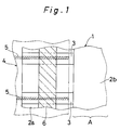
- Fig. 1 is a partially enlarged plan view showing a wiring connection structure in which an electrode 5 formed on such a film-like printed circuit substrate 4 as a tape carrier (tape automated bonding, hereinafter merely called “TAB”) and a flexible printed circuit substrate (hereinafter merely called “FPC”) is connected to another electrode 3 formed on a substrate 2a at the side of a display cell 1 of a liquid crystal display device.
- TAB tape automated bonding
- FPC flexible printed circuit substrate
- the electrode 3 on one substrate 2a which is so formed as to be partially overhung from the display area A of the display cell 1 is, for example, a common electrode, and a segment electrode (not illustrated) is formed on another substrate 2b so arranged as to confront, through a liquid crystal layer (not illustrated), the substrate 2a.
- An anisotropic conductive film 6 is so adhered to the intermediate position on the surface of the portion of the substrate 2a overhung from the display area A that it lies across the electrode 3.
- the film-like printed circuit substrate 4 is so laminated as to secure matching between the electrode 5 and the electrode 3.
- the electrode 3 at the side of the substrate 2a and the electrode 5 at the side of the film-like printed circuit substrate 4 are electrically connected by way of the anisotropic conductive film 6.
- This anisotropic conductive film 6 is a conductive film which can permit the conductivity only in the vertical direction in Fig. 1. Therefore, the adjacent electrodes 3 and 5 are never short-circuited through this anisotropic conductive film 6.
- the electrode 3 on the substrate 2a at the side of the display cell 1 is likely to be peeled off.
- the electrode 3 is not directly formed on the substrate 2a but rather the electrode 3 is formed on an overcoat film comprising resin to shield the colour filter in the case of a colour liquid crystal display device, the electrode 3 is much more likely to be peeled off.
- the electrode 5 of the film-like printed circuit substrate 4 may be reconnected to the electrode 3 of the substrate 2a at the side of the display cell 1 after correcting the positional error or repairing such a fault as wire break, the reliability of the connected portion may be remarkably lowered. Conventionally, re-connection has not been carried out.
- the invention provides a method of wiring connection of a display device in which an array of first electrodes formed on a display substrate of said display device are connected to a corresponding array of second electrodes formed on a wiring substrate by performing a procedure involving positioning the substrates with their said arrays confronting one another and bringing the substrates together to interconnect the respective first and second electrodes thereof, characterized in that the electrode connection position on the display substrate is spaced from the edge of a display section of the display substrate by a space which is sufficient to permit, if necessary, re-connection of the first and second electrodes in the same manner at a different electrode connection position on the display substrate in said space.
- the present invention thus solves the problem of the tendency of the display substrate electrodes to be peeled off, by performing the initial connection at a position suitably removed from the edge of the display area. In this way, there is reserved a part of the display substrate having the electrodes intact for making a new connection, if necessary.
- the substrates previously brought together may be separated.
- the substrates may then be brought together again to form a new connection at said different electrode connection position.
- the invention provides a display device in which an array of first electrodes formed on a display substrate of the display device are connected to a corresponding array of second electrodes formed on a wiring substrate confronting a portion of the display substrate, characterized in that the electrode connection position on the display substrate is spaced from the edge of a display section of the display substrate by a space which is sufficient to permit, if necessary, re-connection of the first and second electrodes at a different electrode connection position on the display substrate in said space.
- Electrode connection position There may be formed on the display substrate, or its associated electrodes, a sign indicating said different electrode connection position.
- the first and second electrodes are interconnected through intermediary anisotropic conductive material.
- the array of second electrodes are distributed among a plurality of said wiring substrates which are individually attachable to the display substrate.
- the wiring substrate affected by the abnormality can be separated from the display substrate.
- the first electrodes formed on the display substrate may be peeled off.
- a connection position which is different from the previous connection position can be used. Therefore, for instance, even though a previously connected portion of the first electrode may have become peeled off, the second electrode can be normally connected to another portion that is not peeled off, in subsequent connection.
- an electrode of a film-like printed circuit substrate can be electrically connected to a portion which is not peeled off of the electrode on the display substrate at the side of the display cell in subsequent connections. So, the reliability of the connected portion is not lowered at all even in subsequent connections. Therefore, it becomes possible to repair the connected points, thereby causing the ratio of completeness of the products to be much heightened.
- the display cell 11 of a colour liquid crystal display device comprises a pair of glass substrates 12a and 12b which confront each other through a liquid crystal layer 16.
- a colour filter 17 is provided on one of the glass substrates 12a, and the colour filter 17 is shielded by an overcoat film 18 consisting of resin.
- An oxidization film 19a such as SiO2, is formed on the overcoat film 18.
- a transparent electrode 20a consisting of ITO (indium tin oxide) film, etc. is formed on this oxidization film 19a, and further a Mo (molybdenum) electrode 21 is formed over the transparent electrode 20a, thereby causing a common electrode 15 to be constituted.
- a plurality of the common electrodes 15 are so formed as to be arranged in parallel with each other on the glass substrate 12a. Then, in the display area A in which the above pair of glass substrates 12a and 12b overlap one another, an orientation film 22a is formed on the front surface of the common electrodes 15.
- a plurality of the transparent electrodes 20b which constitute segment electrodes are formed on the glass substrate 12b in parallel with each other extending in such a direction that they intersect at a right angle the common electrodes 15.
- An oxidization film 19b, such as SiO2 is formed on the transparent electrode 20b, and an orientation film 22b is also formed on the oxidization film 19b.
- a liquid crystal layer 16 is interposed between the orientation film 22a on the glass substrate 12a and the orientation film 22b on the glass substrate 12b and is sealed by means of a sealing member 22.
- the common electrode 15 is formed also on the portion of the glass substrate 12a which extends beyond (i.e. overhangs at) the periphery of the display area A (in the horizontal direction of Fig. 2).
- the segment electrode 20b is formed also on the portion of the glass substrate 12b which extends beyond (i.e. overhangs at) the periphery of the display area A (in the vertical direction of Fig. 2).
- Electrodes 24a formed on a set of such film-like printed circuit substrates 23a as the aforementioned TAB and FPC types are connected by way of an anisotropic conductive film 25a to the common electrodes 15 on the portion of the glass substrate 12a which extends beyond the display area A of the cell 11.
- Chips 26a of integrated circuit hereinafter merely called "IC"
- IC integrated circuit
- the anisotropic conductive film 25a may be such that thin conductor lines are built in, for instance, rubber in parallel with the direction of thickness, or may be such that thin metal particles are uniformly buried in resin and respective metal particles are insulated from each other.
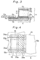
- Fig. 4 shows a structure of connection between the electrodes 24a of the film-like printed circuit substrate 23a and the common electrodes 15 on the glass substrate 12a.
- the anisotropic conductive film 25a is so located that it can be intercrossed with the common electrodes 15 and is adhered thereon.
- the position of attachment of the anisotropic conductive film 25a is set at the edge side of the glass substrate 12a, that is, remotely apart from the display area A, as shown with a one-dashed line in Fig. 4.
- the film-like printed circuit substrate 23a is so overlapped on the glass substrate 12a that the electrodes 24a thereof can be matched to the corresponding common electrodes 15, thereby causing the electrodes 15 and 24a to be connected by means of the anisotropic conductive film 25a.
- the anisotropic conductive film 25a can permit the conductivity only in the vertical direction of Fig. 4. Therefore, it is common to the prior art that the adjacent electrodes 15 and the adjacent electrodes 24a are not short-circuited. In this case, at least such a spacer as to adhere another anisotropic conductive film 25a is secured between the attachment position of the anisotropic conductive film 25a and the edge of the display area A in the first wiring and connection.
- electrodes formed on another set of film-like printed circuit substrates 23b are connected through an anisotropic conductive film 25b to the transparent segment electrodes 20b on the glass substrate 12b.
- IC chips 26b internally having peripheral circuits by which the segment electrodes 20b corresponding to the display cells 11 are driven, are mounted on the film-like printed circuit substrates 23b.
- the film-like printed circuit substrate 23a is peeled off once from the connections thereof, the positional error is corrected and/or the wire break or current leakage is repaired, and the electrodes 15 and 24a are connected again by way of an anisotropic conductive film 25a.
- the attachment position of the anisotropic conductive film 25a on the common electrodes 15 is set to a position (shown with the oblique lines in Fig. 4) closer toward the display area A, thereby avoiding the previous connected portion.
- the setting of a different position, distinguishing the attachment position of the anisotropic conductive film 25a in the first connection from that of the subsequent connection, may be effected by adding a sign at each attachment position to the glass substrate 12a or by forming a part of a sign showing the attachment positions on the pattern of the common electrodes 15.
- connection method can be effected also between the segment electrodes (transparent electrodes) 20b and the electrodes of the other film-like printed circuit substrates 23b.
Landscapes
- Engineering & Computer Science (AREA)
- Physics & Mathematics (AREA)
- Manufacturing & Machinery (AREA)
- Microelectronics & Electronic Packaging (AREA)
- Nonlinear Science (AREA)
- Crystallography & Structural Chemistry (AREA)
- Chemical & Material Sciences (AREA)
- Mathematical Physics (AREA)
- General Physics & Mathematics (AREA)
- Optics & Photonics (AREA)
- Devices For Indicating Variable Information By Combining Individual Elements (AREA)
- Liquid Crystal (AREA)
- Combinations Of Printed Boards (AREA)
Description
- The present invention relates to a method and structure for wiring connection of a display device such as a liquid crystal display device.
- Fig. 1 is a partially enlarged plan view showing a wiring connection structure in which an
electrode 5 formed on such a film-like printed circuit substrate 4 as a tape carrier (tape automated bonding, hereinafter merely called "TAB") and a flexible printed circuit substrate (hereinafter merely called "FPC") is connected to anotherelectrode 3 formed on asubstrate 2a at the side of a display cell 1 of a liquid crystal display device. - In Fig. 1, the
electrode 3 on onesubstrate 2a which is so formed as to be partially overhung from the display area A of the display cell 1 is, for example, a common electrode, and a segment electrode (not illustrated) is formed on anothersubstrate 2b so arranged as to confront, through a liquid crystal layer (not illustrated), thesubstrate 2a. An anisotropicconductive film 6 is so adhered to the intermediate position on the surface of the portion of thesubstrate 2a overhung from the display area A that it lies across theelectrode 3. The film-like printed circuit substrate 4 is so laminated as to secure matching between theelectrode 5 and theelectrode 3. That is, theelectrode 3 at the side of thesubstrate 2a and theelectrode 5 at the side of the film-like printed circuit substrate 4 are electrically connected by way of the anisotropicconductive film 6. This anisotropicconductive film 6 is a conductive film which can permit the conductivity only in the vertical direction in Fig. 1. Therefore, theadjacent electrodes conductive film 6. - In such a wiring connection structure, if the film-like printed circuit substrate 4 is once peeled off from the
substrate 2a at the side of the display cell 1 in order to correct for positional error or to carry out repair, because of, for example, wire break or current leakage, theelectrode 3 on thesubstrate 2a at the side of the display cell 1 is likely to be peeled off. Especially, if theelectrode 3 is not directly formed on thesubstrate 2a but rather theelectrode 3 is formed on an overcoat film comprising resin to shield the colour filter in the case of a colour liquid crystal display device, theelectrode 3 is much more likely to be peeled off. - For this reason, even though the
electrode 5 of the film-like printed circuit substrate 4 may be reconnected to theelectrode 3 of thesubstrate 2a at the side of the display cell 1 after correcting the positional error or repairing such a fault as wire break, the reliability of the connected portion may be remarkably lowered. Conventionally, re-connection has not been carried out. - Actually however, substrates in which positional error or wire break occurs in the connected portions thereof as in the conventional examples are disposed of as defective; the ratio of completeness of the products is thus remarkably lowered, causing the cost of production to be much increased.
- From US-A-4,640,581, it is known to connect a flexible printed circuit board to a terminal section of a display device by carrying out a soldering operation.
- It is therefore an object of the invention to provide a method and structure for wiring connection of a display device by which an electrode of a substrate at the side of a display cell can be reconnected to another electrode of a film-like printed circuit substrate without spoiling the reliability of connection therebetween.
- In one aspect, the invention provides a method of wiring connection of a display device in which an array of first electrodes formed on a display substrate of said display device are connected to a corresponding array of second electrodes formed on a wiring substrate by performing a procedure involving positioning the substrates with their said arrays confronting one another and bringing the substrates together to interconnect the respective first and second electrodes thereof, characterized in that the electrode connection position on the display substrate is spaced from the edge of a display section of the display substrate by a space which is sufficient to permit, if necessary, re-connection of the first and second electrodes in the same manner at a different electrode connection position on the display substrate in said space.
- The present invention thus solves the problem of the tendency of the display substrate electrodes to be peeled off, by performing the initial connection at a position suitably removed from the edge of the display area. In this way, there is reserved a part of the display substrate having the electrodes intact for making a new connection, if necessary.
- When an abnormal connection is formed at the initial electrode connection position, the substrates previously brought together may be separated. The substrates may then be brought together again to form a new connection at said different electrode connection position.
- In another aspect, the invention provides a display device in which an array of first electrodes formed on a display substrate of the display device are connected to a corresponding array of second electrodes formed on a wiring substrate confronting a portion of the display substrate, characterized in that the electrode connection position on the display substrate is spaced from the edge of a display section of the display substrate by a space which is sufficient to permit, if necessary, re-connection of the first and second electrodes at a different electrode connection position on the display substrate in said space.
- There may be formed on the display substrate, or its associated electrodes, a sign indicating said different electrode connection position.
- According to a preferred embodiment of both aspects of the invention, the first and second electrodes are interconnected through intermediary anisotropic conductive material.
- According to a preferred embodiment of both aspects of the invention, the array of second electrodes are distributed among a plurality of said wiring substrates which are individually attachable to the display substrate.
- According to the invention, in the case that any positional error, wire break or current leakage should occur between the first electrodes and the second electrodes when one or more wiring substrates are connected to the display substrate, the wiring substrate affected by the abnormality can be separated from the display substrate. At this time, the first electrodes formed on the display substrate may be peeled off. However, thereafter, a connection position which is different from the previous connection position can be used. Therefore, for instance, even though a previously connected portion of the first electrode may have become peeled off, the second electrode can be normally connected to another portion that is not peeled off, in subsequent connection.
- Thus, according to the method for wiring connection of the display device of the invention, as a repeated connection can be effected at a position different from that of the previously connected portion, an electrode of a film-like printed circuit substrate can be electrically connected to a portion which is not peeled off of the electrode on the display substrate at the side of the display cell in subsequent connections. So, the reliability of the connected portion is not lowered at all even in subsequent connections. Therefore, it becomes possible to repair the connected points, thereby causing the ratio of completeness of the products to be much heightened.
- An embodiment of the invention will now be described, by way of example only, with reference to the accompanying drawings, in which:
- Fig. 1 is a plan view showing an enlarged part of a liquid crystal display device for explanation of a conventional method for wiring connection;
- Fig. 2 is a plan view showing the outline of the composition of a colour liquid crystal display device to which a method for wiring connection according to a preferred embodiment of the invention can be applied;
- Fig. 3 is a sectional view taken along line III - III of Fig. 2; and
- Fig. 4 is an enlarged plan view showing a part marked "IV" in Fig. 2.
- As shown in Fig. 3, the
display cell 11 of a colour liquid crystal display device comprises a pair ofglass substrates liquid crystal layer 16. Acolour filter 17 is provided on one of theglass substrates 12a, and thecolour filter 17 is shielded by anovercoat film 18 consisting of resin. Anoxidization film 19a, such as SiO₂, is formed on theovercoat film 18. Atransparent electrode 20a consisting of ITO (indium tin oxide) film, etc. is formed on thisoxidization film 19a, and further a Mo (molybdenum)electrode 21 is formed over thetransparent electrode 20a, thereby causing acommon electrode 15 to be constituted. A plurality of thecommon electrodes 15 are so formed as to be arranged in parallel with each other on theglass substrate 12a. Then, in the display area A in which the above pair ofglass substrates orientation film 22a is formed on the front surface of thecommon electrodes 15. - A plurality of the
transparent electrodes 20b which constitute segment electrodes are formed on theglass substrate 12b in parallel with each other extending in such a direction that they intersect at a right angle thecommon electrodes 15. Anoxidization film 19b, such as SiO₂, is formed on thetransparent electrode 20b, and anorientation film 22b is also formed on theoxidization film 19b. Aliquid crystal layer 16 is interposed between theorientation film 22a on theglass substrate 12a and theorientation film 22b on theglass substrate 12b and is sealed by means of a sealingmember 22. - The
common electrode 15 is formed also on the portion of theglass substrate 12a which extends beyond (i.e. overhangs at) the periphery of the display area A (in the horizontal direction of Fig. 2). Thesegment electrode 20b is formed also on the portion of theglass substrate 12b which extends beyond (i.e. overhangs at) the periphery of the display area A (in the vertical direction of Fig. 2). -
Electrodes 24a formed on a set of such film-like printedcircuit substrates 23a as the aforementioned TAB and FPC types are connected by way of an anisotropicconductive film 25a to thecommon electrodes 15 on the portion of theglass substrate 12a which extends beyond the display area A of thecell 11.Chips 26a of integrated circuit (hereinafter merely called "IC"), internally having peripheral circuits by which thecommon electrodes 15 corresponding to thedisplay cells 11 are driven, are mounted as shown in Fig. 2. TheseIC chips 26a are connected to thecommon electrodes 15 of thedisplay cell 11 by way of theelectrodes 24a and the anisotropicconductive films 25a. - The anisotropic
conductive film 25a may be such that thin conductor lines are built in, for instance, rubber in parallel with the direction of thickness, or may be such that thin metal particles are uniformly buried in resin and respective metal particles are insulated from each other. - Fig. 4 shows a structure of connection between the
electrodes 24a of the film-likeprinted circuit substrate 23a and thecommon electrodes 15 on theglass substrate 12a. The anisotropicconductive film 25a is so located that it can be intercrossed with thecommon electrodes 15 and is adhered thereon. In the first wiring and connection, the position of attachment of the anisotropicconductive film 25a is set at the edge side of theglass substrate 12a, that is, remotely apart from the display area A, as shown with a one-dashed line in Fig. 4. The film-likeprinted circuit substrate 23a is so overlapped on theglass substrate 12a that theelectrodes 24a thereof can be matched to the correspondingcommon electrodes 15, thereby causing theelectrodes conductive film 25a. The anisotropicconductive film 25a can permit the conductivity only in the vertical direction of Fig. 4. Therefore, it is common to the prior art that theadjacent electrodes 15 and theadjacent electrodes 24a are not short-circuited. In this case, at least such a spacer as to adhere another anisotropicconductive film 25a is secured between the attachment position of the anisotropicconductive film 25a and the edge of the display area A in the first wiring and connection. - Referring to Fig. 2, electrodes formed on another set of film-like printed
circuit substrates 23b are connected through an anisotropicconductive film 25b to thetransparent segment electrodes 20b on theglass substrate 12b.IC chips 26b, internally having peripheral circuits by which thesegment electrodes 20b corresponding to thedisplay cells 11 are driven, are mounted on the film-like printedcircuit substrates 23b. - In the case that any positional error should occur at the connections of the
electrodes circuit substrate 23a is peeled off once from the connections thereof, the positional error is corrected and/or the wire break or current leakage is repaired, and theelectrodes conductive film 25a. At this time, the attachment position of the anisotropicconductive film 25a on thecommon electrodes 15 is set to a position (shown with the oblique lines in Fig. 4) closer toward the display area A, thereby avoiding the previous connected portion. The setting of a different position, distinguishing the attachment position of the anisotropicconductive film 25a in the first connection from that of the subsequent connection, may be effected by adding a sign at each attachment position to theglass substrate 12a or by forming a part of a sign showing the attachment positions on the pattern of thecommon electrodes 15. - In a subsequent connection, even if the
common electrode 15 should become peeled off from theglass substrate 12a at the connected portion when having peeled off the film-like printedcircuit substrate 23a therefrom, in the case that theelectrodes circuit substrate 23a. - The above connection method can be effected also between the segment electrodes (transparent electrodes) 20b and the electrodes of the other film-like printed
circuit substrates 23b. - Also, the preferred embodiment has been described in detail, in relation to the case of a liquid crystal display device. The method of the invention can be applied also to other display devices.
- The invention can be effected in other various modifications and variations without departing from the scope thereof. Therefore, the above mentioned preferred embodiment is merely an example in every aspect.
Claims (8)
- A method of wiring connection of a display device in which an array of first electrodes (15;20b) formed on a display substrate (12a;12b) of said display device are connected to a corresponding array of second electrodes (24a) formed on a wiring substrate (23a;23b) by performing a procedure involving positioning the substrates (12a,23a;12b,23b) with their said arrays confronting one another and bringing the substrates (12a,23a) together to interconnect the respective first and second electrodes (15,24a) thereof, characterized in that the electrode connection position on the display substrate (12a) is spaced from the edge of a display section (A) of the display substrate (12a) by a space which is sufficient to permit, if necessary, re-connection of the first and second electrodes in the same manner at a different electrode connection position on the display substrate in said space.
- The method of claim 1, in which the substrates (12a, 23a) previously brought together are separated because of an abnormal connection formed at the initial electrode connection position on the display substrate (12a), and the substrates (12a,23a) are subsequently brought together again to interconnect the respective first and second electrodes (15,24a) thereof at said different electrode connection position on the display substrate (12a).
- The method of claim 1 or claim 2, wherein the arrays of first (15;20b) and second (24a) electrodes are interconnected through intermediary anisotropic conductive material (25a;25b).
- The method of any one of claims 1 to 3, wherein said array of second electrodes (24a) are distributed among a plurality of said wiring substrates (23a;23b) which are individually attachable to said display substrate (12a;12b).
- A display device in which an array of first electrodes (15;20b) formed on a display substrate (12a;12b) of the display device are connected to a corresponding array of second electrodes (24a) formed on a wiring substrate (23a;23b) confronting a portion of the display substrate, characterized in that the electrode connection position on the display substrate (12a) is spaced from the edge of a display section (A) of the display substrate (12a) by a space which is sufficient to permit, if necessary, re-connection of the first and second electrodes at a different electrode connection position on the display substrate in said space.
- The display device of claim 5, wherein the arrays of first (15;20b) and second (24a) electrodes are interconnected through intermediary anisotropic conductive material (25a;25b).
- The display device of claim 5 or claim 6, wherein said array of second electrodes (24a) are distributed among a plurality of said wiring substrates (23a;23b) which are individually attachable to said display substrate (12a;12b).
- The display device of any one of claims 5 to 7, comprising a sign formed on the display substrate, or its associated electrodes, indicating said different electrode connection position.
Applications Claiming Priority (2)
| Application Number | Priority Date | Filing Date | Title |
|---|---|---|---|
| JP64161/89 | 1989-03-15 | ||
| JP1064161A JP2710977B2 (en) | 1989-03-15 | 1989-03-15 | Display device wiring connection structure and connection method |
Publications (2)
| Publication Number | Publication Date |
|---|---|
| EP0397304A1 EP0397304A1 (en) | 1990-11-14 |
| EP0397304B1 true EP0397304B1 (en) | 1994-08-31 |
Family
ID=13250068
Family Applications (1)
| Application Number | Title | Priority Date | Filing Date |
|---|---|---|---|
| EP90302758A Expired - Lifetime EP0397304B1 (en) | 1989-03-15 | 1990-03-15 | Method and structure for wiring connection of a display device |
Country Status (5)
| Country | Link |
|---|---|
| US (1) | US5112262A (en) |
| EP (1) | EP0397304B1 (en) |
| JP (1) | JP2710977B2 (en) |
| CA (1) | CA2012029C (en) |
| DE (1) | DE69011940T2 (en) |
Families Citing this family (7)
| Publication number | Priority date | Publication date | Assignee | Title |
|---|---|---|---|---|
| JP2814155B2 (en) * | 1990-08-13 | 1998-10-22 | キヤノン株式会社 | Method of forming ITO film pattern and method of manufacturing substrate for liquid crystal display element |
| JP2667744B2 (en) * | 1991-02-28 | 1997-10-27 | ローム株式会社 | Display device electrode connection method |
| JP3018640B2 (en) * | 1991-08-29 | 2000-03-13 | ソニー株式会社 | Circuit connection board structure |
| DE4310112A1 (en) * | 1993-03-27 | 1994-09-29 | Licentia Gmbh | Liquid-crystal display device |
| JPH09148731A (en) * | 1995-11-17 | 1997-06-06 | Fujitsu Ltd | Method for manufacturing connection structure between wiring boards |
| JPH09331142A (en) * | 1996-06-12 | 1997-12-22 | Matsushita Electric Ind Co Ltd | Electronic component mounting method |
| US6379053B1 (en) | 2000-05-30 | 2002-04-30 | Infineon Technologies North America Corp. | Multi-fiber fiber optic connectors |
Family Cites Families (9)
| Publication number | Priority date | Publication date | Assignee | Title |
|---|---|---|---|---|
| JPS5840728B2 (en) * | 1978-08-23 | 1983-09-07 | 株式会社日立製作所 | liquid crystal display device |
| US4304450A (en) * | 1979-12-17 | 1981-12-08 | International Business Machines Corporation | Repair of open circuited gas discharge display panel conductors |
| JPS57135977A (en) * | 1981-02-16 | 1982-08-21 | Canon Kk | Photoelectrical indicator |
| EP0110382A3 (en) * | 1982-12-01 | 1987-01-07 | Asahi Glass Company Ltd. | Display device and process for its production and decal for forming a display panel terminal |
| EP0140619B1 (en) * | 1983-10-14 | 1993-03-17 | Hitachi Chemical Co., Ltd. | Anisotropic-electroconductive adhesive film and circuit connecting method using the same |
| JPS60111068U (en) * | 1983-12-28 | 1985-07-27 | アルプス電気株式会社 | flexible printed circuit board |
| FR2572805A1 (en) * | 1984-11-06 | 1986-05-09 | Thomson Csf | METHOD FOR MEASURING THE CENTERING OF A CYLINDRICAL BAR IN A TRANSPARENT CYLINDRICAL COATING AND DEVICE FOR IMPLEMENTING SAID METHOD |
| KR920000601B1 (en) * | 1986-10-13 | 1992-01-16 | 세미콘덕터 에너지 라보라터리 캄파니 리미티드 | Liquid crystal device manufacturing method |
| JPS63135918A (en) * | 1986-11-27 | 1988-06-08 | Seiko Epson Corp | LCD panel structure |
-
1989
- 1989-03-15 JP JP1064161A patent/JP2710977B2/en not_active Expired - Lifetime
-
1990
- 1990-03-13 US US07/492,915 patent/US5112262A/en not_active Expired - Lifetime
- 1990-03-13 CA CA002012029A patent/CA2012029C/en not_active Expired - Lifetime
- 1990-03-15 EP EP90302758A patent/EP0397304B1/en not_active Expired - Lifetime
- 1990-03-15 DE DE69011940T patent/DE69011940T2/en not_active Expired - Fee Related
Also Published As
| Publication number | Publication date |
|---|---|
| DE69011940T2 (en) | 1995-04-13 |
| EP0397304A1 (en) | 1990-11-14 |
| CA2012029C (en) | 1994-01-04 |
| US5112262A (en) | 1992-05-12 |
| JP2710977B2 (en) | 1998-02-10 |
| CA2012029A1 (en) | 1990-09-15 |
| JPH02242288A (en) | 1990-09-26 |
| DE69011940D1 (en) | 1994-10-06 |
Similar Documents
| Publication | Publication Date | Title |
|---|---|---|
| EP0772073B1 (en) | Liquid crystal display | |
| JP3643110B2 (en) | Manufacturing method of liquid crystal display device | |
| JP3511861B2 (en) | Liquid crystal display panel, inspection method thereof, and method of manufacturing liquid crystal display panel | |
| JP2004095756A (en) | Semiconductor package, method of manufacturing the same, and electronic device | |
| US5112262A (en) | Apparatus and method for electrical connections of a display device | |
| US4934045A (en) | Method of producing electric circuit patterns | |
| CN87107022A (en) | Manufacturing method of liquid crystal device | |
| EP0762137A2 (en) | Liquid crystal display and testing method thereof | |
| JPS6251450B2 (en) | ||
| JPH05203986A (en) | Liquid crystal display device | |
| US7049527B1 (en) | Conductor-pattern testing method, and electro-optical device | |
| JPH07183634A (en) | Panel mounting structure, mounting method, flexible wiring board, and drive IC replacement method | |
| JPS60237431A (en) | Positioning method of display cell | |
| JP3999844B2 (en) | Liquid crystal panel and manufacturing method thereof | |
| GB2180698A (en) | Bonding integrated circuit chips to substrates | |
| KR100477129B1 (en) | Liquid crystal display device with repair line | |
| JPH09113562A (en) | Inspecting method for liquid crystal matrix display panel | |
| KR960000262B1 (en) | LCD with driving integrated circuit mounted on film | |
| JP3846240B2 (en) | Liquid crystal panel inspection apparatus and liquid crystal panel inspection method | |
| JPH01201984A (en) | Wiring substrate | |
| JPH02254422A (en) | Manufacture of active matrix display device | |
| JP2000162632A (en) | Liquid crystal display device | |
| JP2971777B2 (en) | Method for manufacturing cell for liquid crystal display element | |
| JP3610976B2 (en) | Liquid crystal display panel and inspection method thereof | |
| JPH01266585A (en) | Manufacture of electric connecting device |
Legal Events
| Date | Code | Title | Description |
|---|---|---|---|
| PUAI | Public reference made under article 153(3) epc to a published international application that has entered the european phase |
Free format text: ORIGINAL CODE: 0009012 |
|
| AK | Designated contracting states |
Kind code of ref document: A1 Designated state(s): DE GB |
|
| 17P | Request for examination filed |
Effective date: 19901019 |
|
| 17Q | First examination report despatched |
Effective date: 19930224 |
|
| GRAA | (expected) grant |
Free format text: ORIGINAL CODE: 0009210 |
|
| AK | Designated contracting states |
Kind code of ref document: B1 Designated state(s): DE GB |
|
| REF | Corresponds to: |
Ref document number: 69011940 Country of ref document: DE Date of ref document: 19941006 |
|
| PLBE | No opposition filed within time limit |
Free format text: ORIGINAL CODE: 0009261 |
|
| STAA | Information on the status of an ep patent application or granted ep patent |
Free format text: STATUS: NO OPPOSITION FILED WITHIN TIME LIMIT |
|
| 26N | No opposition filed | ||
| REG | Reference to a national code |
Ref country code: GB Ref legal event code: IF02 |
|
| PGFP | Annual fee paid to national office [announced via postgrant information from national office to epo] |
Ref country code: GB Payment date: 20020313 Year of fee payment: 13 |
|
| PGFP | Annual fee paid to national office [announced via postgrant information from national office to epo] |
Ref country code: DE Payment date: 20020327 Year of fee payment: 13 |
|
| PG25 | Lapsed in a contracting state [announced via postgrant information from national office to epo] |
Ref country code: GB Free format text: LAPSE BECAUSE OF NON-PAYMENT OF DUE FEES Effective date: 20030315 |
|
| PG25 | Lapsed in a contracting state [announced via postgrant information from national office to epo] |
Ref country code: DE Free format text: LAPSE BECAUSE OF NON-PAYMENT OF DUE FEES Effective date: 20031001 |
|
| GBPC | Gb: european patent ceased through non-payment of renewal fee |
Effective date: 20030315 |