EP0396332A1 - Process for depositing a ceramic coating on a filament - Google Patents
Process for depositing a ceramic coating on a filament Download PDFInfo
- Publication number
- EP0396332A1 EP0396332A1 EP90304542A EP90304542A EP0396332A1 EP 0396332 A1 EP0396332 A1 EP 0396332A1 EP 90304542 A EP90304542 A EP 90304542A EP 90304542 A EP90304542 A EP 90304542A EP 0396332 A1 EP0396332 A1 EP 0396332A1
- Authority
- EP
- European Patent Office
- Prior art keywords
- indium
- filament
- mercury
- mixture
- amalgam
- Prior art date
- Legal status (The legal status is an assumption and is not a legal conclusion. Google has not performed a legal analysis and makes no representation as to the accuracy of the status listed.)
- Granted
Links
Images
Classifications
-
- C—CHEMISTRY; METALLURGY
- C23—COATING METALLIC MATERIAL; COATING MATERIAL WITH METALLIC MATERIAL; CHEMICAL SURFACE TREATMENT; DIFFUSION TREATMENT OF METALLIC MATERIAL; COATING BY VACUUM EVAPORATION, BY SPUTTERING, BY ION IMPLANTATION OR BY CHEMICAL VAPOUR DEPOSITION, IN GENERAL; INHIBITING CORROSION OF METALLIC MATERIAL OR INCRUSTATION IN GENERAL
- C23C—COATING METALLIC MATERIAL; COATING MATERIAL WITH METALLIC MATERIAL; SURFACE TREATMENT OF METALLIC MATERIAL BY DIFFUSION INTO THE SURFACE, BY CHEMICAL CONVERSION OR SUBSTITUTION; COATING BY VACUUM EVAPORATION, BY SPUTTERING, BY ION IMPLANTATION OR BY CHEMICAL VAPOUR DEPOSITION, IN GENERAL
- C23C16/00—Chemical coating by decomposition of gaseous compounds, without leaving reaction products of surface material in the coating, i.e. chemical vapour deposition [CVD] processes
- C23C16/44—Chemical coating by decomposition of gaseous compounds, without leaving reaction products of surface material in the coating, i.e. chemical vapour deposition [CVD] processes characterised by the method of coating
- C23C16/46—Chemical coating by decomposition of gaseous compounds, without leaving reaction products of surface material in the coating, i.e. chemical vapour deposition [CVD] processes characterised by the method of coating characterised by the method used for heating the substrate
-
- C—CHEMISTRY; METALLURGY
- C23—COATING METALLIC MATERIAL; COATING MATERIAL WITH METALLIC MATERIAL; CHEMICAL SURFACE TREATMENT; DIFFUSION TREATMENT OF METALLIC MATERIAL; COATING BY VACUUM EVAPORATION, BY SPUTTERING, BY ION IMPLANTATION OR BY CHEMICAL VAPOUR DEPOSITION, IN GENERAL; INHIBITING CORROSION OF METALLIC MATERIAL OR INCRUSTATION IN GENERAL
- C23C—COATING METALLIC MATERIAL; COATING MATERIAL WITH METALLIC MATERIAL; SURFACE TREATMENT OF METALLIC MATERIAL BY DIFFUSION INTO THE SURFACE, BY CHEMICAL CONVERSION OR SUBSTITUTION; COATING BY VACUUM EVAPORATION, BY SPUTTERING, BY ION IMPLANTATION OR BY CHEMICAL VAPOUR DEPOSITION, IN GENERAL
- C23C16/00—Chemical coating by decomposition of gaseous compounds, without leaving reaction products of surface material in the coating, i.e. chemical vapour deposition [CVD] processes
- C23C16/44—Chemical coating by decomposition of gaseous compounds, without leaving reaction products of surface material in the coating, i.e. chemical vapour deposition [CVD] processes characterised by the method of coating
- C23C16/54—Apparatus specially adapted for continuous coating
- C23C16/545—Apparatus specially adapted for continuous coating for coating elongated substrates
Definitions
- the present invention relates to a process for depositing a ceramic coating on a filament.
- the present invention provides a process for depositing a ceramic coating on a filament, which comprises heating the filament by passage of an electric current via at least two electrodes, and passing the heated filament through a deposition chamber containing gases which on contact with the hot filament deposit the required coating; characterised in that after deposition of the coating, the coated filament passes through an electrode containing a liquid metal mixture which is a mercury/indium or mercury/cadmium amalgam or a gallium/indium mixture.
- the amount of indium or cadmium present in the amalgam is preferably in the range of from 0.5 to 8%, preferably from 1 to 6%, by weight. If the liquid metal mixture is a gallium/indium mixture, this preferably contains from 10 to 25% w of indium, and is preferably the eutectic mixture. Preferably the liquid metal mixture is a mercury/indium amalgam.
- the design of electrode is not important, any known design being suitable for use with a metal mixture in accordance with the invention.
- the process of the present invention may be used for depositing any desired ceramic coating on a filament.
- the filament may for example be tungsten or carbon.
- Typical ceramic coatings include boron and silicon carbide.
- the process may of course be used to deposit an additional ceramic layer over an existing ceramic layer, for example boron over silicon carbide or silicon carbide over boron.
- US Patents 4068037, 4315968, 4340636, 4481257, 4628002 and 4702960 describe various ceramic-coated filaments which can be produced by the process of the present invention. The process is particularly advantageous when depositing silicon carbide on a tungsten filament.
- Suitable gases used to deposit silicon carbide include haloalkylsilanes, such as methyltrichlorosilane, methyldichlorosilane or dimethyldichlorosilane, together with hydrogen.
- silicon tetrachloride or monosilane together with a hydrocarbon, for example methane, and hydrogen may be used.
- a minor amount of carbon dioxide is included in the gases.
- the gases Preferably the gases contain less than 2%, especially less than 1%, but more than 0.05%, preferably more than 0.1%, by volume of carbon dioxide.
- At least one electrode through which the coated filament passes contains the defined liquid metal mixture.
- An apparatus for carrying out the deposition process may of course contain a number of electrodes, any or all of which may contain the defined liquid metal mixture.
- a particular process may involve a number of discrete deposition zones.
- a process may incorporate one or more cleaning zones in which the filament is cleaned prior to deposition of a coating. If in such a process, a filament having a ceramic coating passes through more than one electrode, each such electrode may contain the defined liquid metal mixture.
- the invention also provides an apparatus for depositing a ceramic coating on a filament, which comprises a deposition chamber and at least two electrodes, the arrangement being such that in use, a filament is heated by passage of an electric current via the electrodes, the heated filament being passed through the deposition chamber containing gases which on contact with the hot filament deposit the required coating; characterized in that the electrode through which, in use, the filament passes after deposition, contains a liquid metal mixture which is a mercury/indium or mercury/cadmium amalgam or a gallium/indium mixture.
- the products produced by the process of the invention are of high quality.
- the use of the defined metal mixture leads to a product with improved tensile strength.
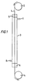
- FIG. 1 shows an apparatus which may be used to carry out the process of the invention.
- a filament 1 for example tungsten, is fed from a supply 2 via a tube 3 to a store 4.
- the filament 1 passes through a mercury electrode 5 at the upper end of the tube 3, and an electrode 6 at the lower end of the tube 3, which contains a mercury/indium or mercury/cadmium amalgam or a liquid gallium/indium mixture.
- the electrodes 5 and 6 form part of an electric current circuit (not shown) which supplies an electric heating current to the filament 1. Gases which on contact with the hot filament deposit the desired ceramic coating, are fed into the tube 2 via inlet 7, and removed via outlet 8.
- the liquid metal mixture in electrode 6 may be replaced by pure mercury.
- arcing occurs at electrode 6. In some runs, this causes the filament 1 to break. In other runs, the coating deposited on the finished product is pitted and of much reduced tensile strength.
Landscapes
- Chemical & Material Sciences (AREA)
- General Chemical & Material Sciences (AREA)
- Chemical Kinetics & Catalysis (AREA)
- Engineering & Computer Science (AREA)
- Materials Engineering (AREA)
- Mechanical Engineering (AREA)
- Metallurgy (AREA)
- Organic Chemistry (AREA)
- Chemical Vapour Deposition (AREA)
- Chemical Or Physical Treatment Of Fibers (AREA)
- Battery Electrode And Active Subsutance (AREA)
- Physical Vapour Deposition (AREA)
Abstract
Description
- The present invention relates to a process for depositing a ceramic coating on a filament.
- It is well known to deposit ceramic coatings on filaments using chemical vapour deposition (CVD) techniques. In a typical process, a heated filament is passed continuously through a deposition chamber. Conveniently, the filament is heated by passage of an electric current, and the electric current is supplied via mercury electrodes through which the wire passes. Such processes are described in, for example, US 4127659 and US 3622369.
- Problems can arise when the surface of the filament presented to mercury in an electrode is of low conductivity. For example, in the case where a tungsten filament is coated with silicon carbide, it is generally easy to pass current to the tungsten filament at an electrode at the entry to the deposition chamber, and much more difficult to pass current at an electrode at the exit from the deposition chamber, when the tungsten filament carries a layer of silicon carbide.
- We have now found that the problems can be reduced and a high quality product produced by using a defined metal mixture rather than pure mercury in an electrode.
- Accordingly, the present invention provides a process for depositing a ceramic coating on a filament, which comprises heating the filament by passage of an electric current via at least two electrodes, and passing the heated filament through a deposition chamber containing gases which on contact with the hot filament deposit the required coating; characterised in that after deposition of the coating, the coated filament passes through an electrode containing a liquid metal mixture which is a mercury/indium or mercury/cadmium amalgam or a gallium/indium mixture.
- If the liquid metal mixture is a mercury/indium or mercury/cadmium amalgam, the amount of indium or cadmium present in the amalgam is preferably in the range of from 0.5 to 8%, preferably from 1 to 6%, by weight. If the liquid metal mixture is a gallium/indium mixture, this preferably contains from 10 to 25% w of indium, and is preferably the eutectic mixture. Preferably the liquid metal mixture is a mercury/indium amalgam.
- The design of electrode is not important, any known design being suitable for use with a metal mixture in accordance with the invention. In some designs of CVD reactor, there is a pressure difference between the upper and lower surfaces of the conducting pool. In such a case, it is desirable for the design of the electrode to incorporate a pressure equalisation device, to stop gases bubbling through the pool.
- The process of the present invention may be used for depositing any desired ceramic coating on a filament. The filament may for example be tungsten or carbon. Typical ceramic coatings include boron and silicon carbide. The process may of course be used to deposit an additional ceramic layer over an existing ceramic layer, for example boron over silicon carbide or silicon carbide over boron. US Patents 4068037, 4315968, 4340636, 4481257, 4628002 and 4702960 describe various ceramic-coated filaments which can be produced by the process of the present invention. The process is particularly advantageous when depositing silicon carbide on a tungsten filament. Suitable gases used to deposit silicon carbide include haloalkylsilanes, such as methyltrichlorosilane, methyldichlorosilane or dimethyldichlorosilane, together with hydrogen. Alternatively, silicon tetrachloride or monosilane together with a hydrocarbon, for example methane, and hydrogen, may be used. Advantageously, a minor amount of carbon dioxide is included in the gases. Preferably the gases contain less than 2%, especially less than 1%, but more than 0.05%, preferably more than 0.1%, by volume of carbon dioxide.
- In the process according to the invention, at least one electrode through which the coated filament passes contains the defined liquid metal mixture. An apparatus for carrying out the deposition process may of course contain a number of electrodes, any or all of which may contain the defined liquid metal mixture. A particular process may involve a number of discrete deposition zones. In addition, a process may incorporate one or more cleaning zones in which the filament is cleaned prior to deposition of a coating. If in such a process, a filament having a ceramic coating passes through more than one electrode, each such electrode may contain the defined liquid metal mixture.
- The invention also provides an apparatus for depositing a ceramic coating on a filament, which comprises a deposition chamber and at least two electrodes, the arrangement being such that in use, a filament is heated by passage of an electric current via the electrodes, the heated filament being passed through the deposition chamber containing gases which on contact with the hot filament deposit the required coating; characterized in that the electrode through which, in use, the filament passes after deposition, contains a liquid metal mixture which is a mercury/indium or mercury/cadmium amalgam or a gallium/indium mixture.
- The products produced by the process of the invention are of high quality. In particular, the use of the defined metal mixture leads to a product with improved tensile strength.
- The process and apparatus of the invention are illustrated in the accompanying drawing, Figure 1, which shows an apparatus which may be used to carry out the process of the invention. A filament 1, for example tungsten, is fed from a supply 2 via a tube 3 to a store 4. The filament 1 passes through a
mercury electrode 5 at the upper end of the tube 3, and an electrode 6 at the lower end of the tube 3, which contains a mercury/indium or mercury/cadmium amalgam or a liquid gallium/indium mixture. Theelectrodes 5 and 6 form part of an electric current circuit (not shown) which supplies an electric heating current to the filament 1. Gases which on contact with the hot filament deposit the desired ceramic coating, are fed into the tube 2 via inlet 7, and removed via outlet 8. - In comparison experiments, the liquid metal mixture in electrode 6 may be replaced by pure mercury. On start-up of the process, arcing occurs at electrode 6. In some runs, this causes the filament 1 to break. In other runs, the coating deposited on the finished product is pitted and of much reduced tensile strength.
Claims (11)
Applications Claiming Priority (2)
| Application Number | Priority Date | Filing Date | Title |
|---|---|---|---|
| GB898910181A GB8910181D0 (en) | 1989-05-04 | 1989-05-04 | Process for depositing a ceramic coating on a filament |
| GB8910181 | 1989-05-04 |
Publications (2)
| Publication Number | Publication Date |
|---|---|
| EP0396332A1 true EP0396332A1 (en) | 1990-11-07 |
| EP0396332B1 EP0396332B1 (en) | 1993-02-03 |
Family
ID=10656164
Family Applications (1)
| Application Number | Title | Priority Date | Filing Date |
|---|---|---|---|
| EP90304542A Expired - Lifetime EP0396332B1 (en) | 1989-05-04 | 1990-04-26 | Process for depositing a ceramic coating on a filament |
Country Status (7)
| Country | Link |
|---|---|
| US (1) | US5156883A (en) |
| EP (1) | EP0396332B1 (en) |
| JP (1) | JP2966034B2 (en) |
| AU (1) | AU618671B2 (en) |
| CA (1) | CA2015126C (en) |
| DE (1) | DE69000850T2 (en) |
| GB (1) | GB8910181D0 (en) |
Cited By (4)
| Publication number | Priority date | Publication date | Assignee | Title |
|---|---|---|---|---|
| AU655033B2 (en) * | 1991-06-27 | 1994-12-01 | Scientific Ecology Group, Inc., The | Method for decontaminating soil containing resins |
| RU2471885C1 (en) * | 2011-12-27 | 2013-01-10 | Российская Федерация, от имени которой выступает Министерство промышленности и торговли Российской Федерации (МИНПРОМТОРГ РОССИИ ) | Device to produce silicon-carbide fibers |
| RU2477338C1 (en) * | 2011-12-28 | 2013-03-10 | Федеральное государственное унитарное предприятие "Государственный ордена Трудового Красного Знамени научно-исследовательский институт химии и технологии элементоорганических соединений" (ФГУП ГНИИХТЭОС) | Device for obtaining boron fibres |
| US9187828B2 (en) | 2008-08-22 | 2015-11-17 | Tisics Limited | Coated filaments and their manufacture |
Families Citing this family (1)
| Publication number | Priority date | Publication date | Assignee | Title |
|---|---|---|---|---|
| US5609912A (en) * | 1995-09-08 | 1997-03-11 | Georgia Tech Research Corp. | Ceramic fabric forming method |
Citations (6)
| Publication number | Priority date | Publication date | Assignee | Title |
|---|---|---|---|---|
| DE1696621A1 (en) * | 1967-02-24 | 1971-11-18 | United Aircraft Corp | Process for the production of coatings and wires from stoechiometric silicon carbide |
| FR2170952A1 (en) * | 1972-02-09 | 1973-09-21 | Armines | Coating a wire with silicon carbide - by joule heating in a gaseous atmosphere of precursors |
| US4068037A (en) * | 1976-01-02 | 1978-01-10 | Avco Corporation | Silicon carbide filaments and method |
| US4315968A (en) * | 1980-02-06 | 1982-02-16 | Avco Corporation | Silicon coated silicon carbide filaments and method |
| DE3130117A1 (en) * | 1980-07-30 | 1982-06-09 | Avco Corp., 06830 Greenwich, Conn. | SURFACE TREATMENT OF SILICON CARBIDE |
| US4481257A (en) * | 1979-11-26 | 1984-11-06 | Avco Corporation | Boron coated silicon carbide filaments |
Family Cites Families (5)
| Publication number | Priority date | Publication date | Assignee | Title |
|---|---|---|---|---|
| US3479205A (en) * | 1966-10-14 | 1969-11-18 | Gen Electric | Process for producing boron filament |
| US3367304A (en) * | 1967-03-13 | 1968-02-06 | Dow Corning | Deposition chamber for manufacture of refractory coated filaments |
| US4415609A (en) * | 1980-07-30 | 1983-11-15 | Avco Corporation | Method of applying a carbon-rich surface layer to a silicon carbide filament |
| US4358473A (en) * | 1981-05-22 | 1982-11-09 | Avco Corporation | Process control system |
| US4437041A (en) * | 1981-11-12 | 1984-03-13 | General Electric Company | Amalgam heating system for solenoidal electric field lamps |
-
1989
- 1989-05-04 GB GB898910181A patent/GB8910181D0/en active Pending
-
1990
- 1990-04-18 AU AU53299/90A patent/AU618671B2/en not_active Ceased
- 1990-04-23 CA CA002015126A patent/CA2015126C/en not_active Expired - Lifetime
- 1990-04-26 EP EP90304542A patent/EP0396332B1/en not_active Expired - Lifetime
- 1990-04-26 DE DE9090304542T patent/DE69000850T2/en not_active Expired - Fee Related
- 1990-04-27 JP JP2110686A patent/JP2966034B2/en not_active Expired - Fee Related
-
1991
- 1991-07-02 US US07/727,318 patent/US5156883A/en not_active Expired - Lifetime
Patent Citations (6)
| Publication number | Priority date | Publication date | Assignee | Title |
|---|---|---|---|---|
| DE1696621A1 (en) * | 1967-02-24 | 1971-11-18 | United Aircraft Corp | Process for the production of coatings and wires from stoechiometric silicon carbide |
| FR2170952A1 (en) * | 1972-02-09 | 1973-09-21 | Armines | Coating a wire with silicon carbide - by joule heating in a gaseous atmosphere of precursors |
| US4068037A (en) * | 1976-01-02 | 1978-01-10 | Avco Corporation | Silicon carbide filaments and method |
| US4481257A (en) * | 1979-11-26 | 1984-11-06 | Avco Corporation | Boron coated silicon carbide filaments |
| US4315968A (en) * | 1980-02-06 | 1982-02-16 | Avco Corporation | Silicon coated silicon carbide filaments and method |
| DE3130117A1 (en) * | 1980-07-30 | 1982-06-09 | Avco Corp., 06830 Greenwich, Conn. | SURFACE TREATMENT OF SILICON CARBIDE |
Cited By (4)
| Publication number | Priority date | Publication date | Assignee | Title |
|---|---|---|---|---|
| AU655033B2 (en) * | 1991-06-27 | 1994-12-01 | Scientific Ecology Group, Inc., The | Method for decontaminating soil containing resins |
| US9187828B2 (en) | 2008-08-22 | 2015-11-17 | Tisics Limited | Coated filaments and their manufacture |
| RU2471885C1 (en) * | 2011-12-27 | 2013-01-10 | Российская Федерация, от имени которой выступает Министерство промышленности и торговли Российской Федерации (МИНПРОМТОРГ РОССИИ ) | Device to produce silicon-carbide fibers |
| RU2477338C1 (en) * | 2011-12-28 | 2013-03-10 | Федеральное государственное унитарное предприятие "Государственный ордена Трудового Красного Знамени научно-исследовательский институт химии и технологии элементоорганических соединений" (ФГУП ГНИИХТЭОС) | Device for obtaining boron fibres |
Also Published As
| Publication number | Publication date |
|---|---|
| JP2966034B2 (en) | 1999-10-25 |
| EP0396332B1 (en) | 1993-02-03 |
| DE69000850D1 (en) | 1993-03-18 |
| CA2015126C (en) | 1999-08-31 |
| GB8910181D0 (en) | 1989-06-21 |
| US5156883A (en) | 1992-10-20 |
| JPH0320471A (en) | 1991-01-29 |
| AU618671B2 (en) | 1992-01-02 |
| CA2015126A1 (en) | 1990-11-04 |
| AU5329990A (en) | 1990-11-08 |
| DE69000850T2 (en) | 1993-05-19 |
Similar Documents
| Publication | Publication Date | Title |
|---|---|---|
| US5439492A (en) | Fine grain diamond workpieces | |
| US5425842A (en) | Method of manufacturing a semiconductor device using a chemical vapour deposition process with plasma cleaning of the reactor chamber | |
| EP1127955B1 (en) | Low resistivity silicon carbide | |
| KR940011007B1 (en) | Plasma processing method and products thereof | |
| WO1996018756A1 (en) | A PA-CVD PROCESS FOR DEPOSITION OF A SOLID METAL-CONTAINING FILM ONTO A SUBSTRATE CONTAINING AT LEAST 50 % of Fe or WC | |
| EP0396332B1 (en) | Process for depositing a ceramic coating on a filament | |
| US20030021595A1 (en) | Apparatus and method for vaporizing a liquid chemical | |
| Rie et al. | Investigation of PA-CVD of TiN: relations between process parameters, spectroscopic measurements and layer properties | |
| JPH0710519A (en) | Method for preparation of disilane and reactor for use in said method | |
| WO2003017737A2 (en) | Cascade arc plasma and abrasion resistant coatings made therefrom | |
| RU2114932C1 (en) | Ceramic coated threads and method of coating deposition | |
| EP0396333B1 (en) | Process for depositing a silicon carbide coating on a filament | |
| US5221353A (en) | Apparatus for depositing a ceramic coating on a filament | |
| GB2169443A (en) | Apparatus for processing semiconductors wafers | |
| US3985917A (en) | Method of depositing material on a heated substrate | |
| US3536522A (en) | Method for purification of reaction gases | |
| EP0574075B1 (en) | Method of manufacturing a semiconductor device by means of a chemical vapour deposition | |
| JP2825992B2 (en) | Manufacturing method of ceramic fiber | |
| US3479205A (en) | Process for producing boron filament | |
| EP0443659B1 (en) | A process for applying a coating on powdery particles and a process for the production of metallic objects by using these particles | |
| US6623802B1 (en) | Process and installation for forming a layer on a substrate | |
| KR100284630B1 (en) | Method of manufacturing semiconductor device by chemical vapor deposition | |
| JPS58174568A (en) | Formation of film of metal compound | |
| AU782275B2 (en) | Method and implementing device for a chemical reaction | |
| CN1092820A (en) | The apparatus and method of sedimentation of solid material, particularly fine particles and the application of this method |
Legal Events
| Date | Code | Title | Description |
|---|---|---|---|
| PUAI | Public reference made under article 153(3) epc to a published international application that has entered the european phase |
Free format text: ORIGINAL CODE: 0009012 |
|
| AK | Designated contracting states |
Kind code of ref document: A1 Designated state(s): DE FR GB IT NL SE |
|
| 17P | Request for examination filed |
Effective date: 19901227 |
|
| 17Q | First examination report despatched |
Effective date: 19920519 |
|
| GRAA | (expected) grant |
Free format text: ORIGINAL CODE: 0009210 |
|
| AK | Designated contracting states |
Kind code of ref document: B1 Designated state(s): DE FR GB IT NL SE |
|
| ITF | It: translation for a ep patent filed | ||
| REF | Corresponds to: |
Ref document number: 69000850 Country of ref document: DE Date of ref document: 19930318 |
|
| ET | Fr: translation filed | ||
| PLBE | No opposition filed within time limit |
Free format text: ORIGINAL CODE: 0009261 |
|
| 26N | No opposition filed | ||
| REG | Reference to a national code |
Ref country code: GB Ref legal event code: 732E |
|
| EAL | Se: european patent in force in sweden |
Ref document number: 90304542.5 |
|
| REG | Reference to a national code |
Ref country code: GB Ref legal event code: 732E |
|
| REG | Reference to a national code |
Ref country code: GB Ref legal event code: IF02 |
|
| PGFP | Annual fee paid to national office [announced via postgrant information from national office to epo] |
Ref country code: SE Payment date: 20080319 Year of fee payment: 19 Ref country code: GB Payment date: 20080320 Year of fee payment: 19 |
|
| PGFP | Annual fee paid to national office [announced via postgrant information from national office to epo] |
Ref country code: DE Payment date: 20080320 Year of fee payment: 19 Ref country code: FR Payment date: 20080313 Year of fee payment: 19 |
|
| PGFP | Annual fee paid to national office [announced via postgrant information from national office to epo] |
Ref country code: IT Payment date: 20080329 Year of fee payment: 19 |
|
| PGFP | Annual fee paid to national office [announced via postgrant information from national office to epo] |
Ref country code: NL Payment date: 20080325 Year of fee payment: 19 |
|
| EUG | Se: european patent has lapsed | ||
| GBPC | Gb: european patent ceased through non-payment of renewal fee |
Effective date: 20090426 |
|
| NLV4 | Nl: lapsed or anulled due to non-payment of the annual fee |
Effective date: 20091101 |
|
| REG | Reference to a national code |
Ref country code: FR Ref legal event code: ST Effective date: 20091231 |
|
| PG25 | Lapsed in a contracting state [announced via postgrant information from national office to epo] |
Ref country code: DE Free format text: LAPSE BECAUSE OF NON-PAYMENT OF DUE FEES Effective date: 20091103 |
|
| PG25 | Lapsed in a contracting state [announced via postgrant information from national office to epo] |
Ref country code: NL Free format text: LAPSE BECAUSE OF NON-PAYMENT OF DUE FEES Effective date: 20091101 |
|
| PG25 | Lapsed in a contracting state [announced via postgrant information from national office to epo] |
Ref country code: FR Free format text: LAPSE BECAUSE OF NON-PAYMENT OF DUE FEES Effective date: 20091222 Ref country code: GB Free format text: LAPSE BECAUSE OF NON-PAYMENT OF DUE FEES Effective date: 20090426 |
|
| PG25 | Lapsed in a contracting state [announced via postgrant information from national office to epo] |
Ref country code: IT Free format text: LAPSE BECAUSE OF NON-PAYMENT OF DUE FEES Effective date: 20090426 |
|
| PG25 | Lapsed in a contracting state [announced via postgrant information from national office to epo] |
Ref country code: SE Free format text: LAPSE BECAUSE OF NON-PAYMENT OF DUE FEES Effective date: 20090427 |