US4415609A - Method of applying a carbon-rich surface layer to a silicon carbide filament - Google Patents
Method of applying a carbon-rich surface layer to a silicon carbide filament Download PDFInfo
- Publication number
- US4415609A US4415609A US06/374,992 US37499282A US4415609A US 4415609 A US4415609 A US 4415609A US 37499282 A US37499282 A US 37499282A US 4415609 A US4415609 A US 4415609A
- Authority
- US
- United States
- Prior art keywords
- carbon
- silicon carbide
- filament
- silane
- rich
- Prior art date
- Legal status (The legal status is an assumption and is not a legal conclusion. Google has not performed a legal analysis and makes no representation as to the accuracy of the status listed.)
- Expired - Lifetime
Links
Images

Classifications
-
- H—ELECTRICITY
- H05—ELECTRIC TECHNIQUES NOT OTHERWISE PROVIDED FOR
- H05B—ELECTRIC HEATING; ELECTRIC LIGHT SOURCES NOT OTHERWISE PROVIDED FOR; CIRCUIT ARRANGEMENTS FOR ELECTRIC LIGHT SOURCES, IN GENERAL
- H05B6/00—Heating by electric, magnetic or electromagnetic fields
- H05B6/64—Heating using microwaves
- H05B6/78—Arrangements for continuous movement of material
- H05B6/788—Arrangements for continuous movement of material wherein an elongated material is moved by applying a mechanical tension to it
-
- C—CHEMISTRY; METALLURGY
- C04—CEMENTS; CONCRETE; ARTIFICIAL STONE; CERAMICS; REFRACTORIES
- C04B—LIME, MAGNESIA; SLAG; CEMENTS; COMPOSITIONS THEREOF, e.g. MORTARS, CONCRETE OR LIKE BUILDING MATERIALS; ARTIFICIAL STONE; CERAMICS; REFRACTORIES; TREATMENT OF NATURAL STONE
- C04B41/00—After-treatment of mortars, concrete, artificial stone or ceramics; Treatment of natural stone
- C04B41/45—Coating or impregnating, e.g. injection in masonry, partial coating of green or fired ceramics, organic coating compositions for adhering together two concrete elements
- C04B41/4584—Coating or impregnating of particulate or fibrous ceramic material
-
- C—CHEMISTRY; METALLURGY
- C04—CEMENTS; CONCRETE; ARTIFICIAL STONE; CERAMICS; REFRACTORIES
- C04B—LIME, MAGNESIA; SLAG; CEMENTS; COMPOSITIONS THEREOF, e.g. MORTARS, CONCRETE OR LIKE BUILDING MATERIALS; ARTIFICIAL STONE; CERAMICS; REFRACTORIES; TREATMENT OF NATURAL STONE
- C04B41/00—After-treatment of mortars, concrete, artificial stone or ceramics; Treatment of natural stone
- C04B41/80—After-treatment of mortars, concrete, artificial stone or ceramics; Treatment of natural stone of only ceramics
- C04B41/81—Coating or impregnation
-
- C—CHEMISTRY; METALLURGY
- C23—COATING METALLIC MATERIAL; COATING MATERIAL WITH METALLIC MATERIAL; CHEMICAL SURFACE TREATMENT; DIFFUSION TREATMENT OF METALLIC MATERIAL; COATING BY VACUUM EVAPORATION, BY SPUTTERING, BY ION IMPLANTATION OR BY CHEMICAL VAPOUR DEPOSITION, IN GENERAL; INHIBITING CORROSION OF METALLIC MATERIAL OR INCRUSTATION IN GENERAL
- C23C—COATING METALLIC MATERIAL; COATING MATERIAL WITH METALLIC MATERIAL; SURFACE TREATMENT OF METALLIC MATERIAL BY DIFFUSION INTO THE SURFACE, BY CHEMICAL CONVERSION OR SUBSTITUTION; COATING BY VACUUM EVAPORATION, BY SPUTTERING, BY ION IMPLANTATION OR BY CHEMICAL VAPOUR DEPOSITION, IN GENERAL
- C23C16/00—Chemical coating by decomposition of gaseous compounds, without leaving reaction products of surface material in the coating, i.e. chemical vapour deposition [CVD] processes
- C23C16/22—Chemical coating by decomposition of gaseous compounds, without leaving reaction products of surface material in the coating, i.e. chemical vapour deposition [CVD] processes characterised by the deposition of inorganic material, other than metallic material
- C23C16/30—Deposition of compounds, mixtures or solid solutions, e.g. borides, carbides, nitrides
- C23C16/32—Carbides
- C23C16/325—Silicon carbide
Definitions
- silicon carbide shall mean stoichiometric silicon carbide.
- Carbon-rich silicon carbide shall mean deposits in which the ratio of silicon to carbon shall be in the range of 0+to 1.
- High-strength and/or high-modulus filaments or strips shall mean structures having a tensile strength of 300 ksi or greater and a tensile modulus of 40,000 ksi or greater.
- the present invention is applicable to silicon carbide and carbon surfaces of all shapes and sizes. It is particularly important for filaments, thin strips, and the like. The following discussion will be directed to filaments as a typical example.
- Composite materials in plastic or metal matrices reinforced with high-strength, high-modulus filaments such as boron and silicon carbide are finding increased popularity in structural applications.
- these types of composites are useful where high-strength and stiffness with accompanying low weight is desired.
- the present state-of-the-art silicon carbide filament or thin strip contains a refractory core, generally tungsten or carbon.
- the core may include an intermediate buffer zone followed by a relatively thick layer of silicon carbide.
- the silicon carbide and buffer zone are made by means of hydrogen reduction and chemical vapor deposition processes wherein gases containing silicon and carbon are decomposed and deposited on the core.
- the thickness of the silicon carbide coating is directly related to the deposition time and temperature.
- silicon carbide coatings are in connection with high-strength, high-modulus silicon carbide filaments of the type described in U.S. Pat. No. 4,068,037.
- this patent there is described a silicon carbide filament formed on a carbonaceous core.
- the silicon carbide coating is deposited on a tungsten core.
- the aforementioned referenced patent U.S. Pat. No. 4,068,037, is the closest art known to Applicants in relation to the present invention.
- the filament described in the referenced patent represents the state of the art.
- the filament described in the patent contains a carbon-rich silicon carbide outer coating which is important for maintaining overall filament strength and stiffness.
- this outer coating makes it very difficult to incorporate these filaments within metal matrices such as aluminum, titanium, as well as epoxy matrices because the matrix material does not bond well to the carbon-rich outer layer.
- the outer carbon-rich silicon carbide layer of the state-of-the-art silicon carbide filament discussed above has been physically characterized as a layer where the ratio of silicon to carbon varies from one at the interface of the carbon-rich layer with the stoichiometric silicon carbide layer to zero at the exterior surface of the filament.
- the exterior surface of the carbon-rich layer is essentially pure carbon.
- a surface treatment for stoichiometric silicon carbide and/or carbon comprising a carbon-rich silicon carbide layer overcoating the stoichiometric silicon carbide or carbon.
- the ratio of silicon to carbon of the carbon-rich layer varies from one at the interface with stoichiometric silicon carbide to near zero at the interior to a value substantially greater than zero at the surface remote from said interface.
- the carbon rich silicon carbide treatment for carbon surface has a silicon to carbon ratio of zero at the carbon surface to a value greater than zero in the remote surface.
- silicon carbide is particularly sensitive to the presence of non-stoichiometric silicon carbide or impurities.
- I. T. Kendall Journal of Chemical Physics, Vol. 21, pg. 821 (1953). Since both Kendall and K. Arnt & E. Hausmanne in Zeits Anorg Chem., Vol. 215, pg. 66 (1933) have found no evidence of non-stoichiometric silicon carbide, it is hypothesized that the excess carbon appears in the silicon carbide as an impurity.
- the properties of silicon carbide are particularly sensitive to the presence of impurities such as carbon.
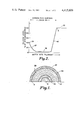
- FIG. 1 is a cross-sectional representation of silicon carbide filament embodying the principals of the present invention
- FIG. 2 is a curve which is useful in describing the invention.
- FIG. 3 is a schematic representation of a reactor for making silicon carbide filament.
- This invention will be described within the context of making silicon carbide filament.
- the invention is operative, irrespective of the structure and composition of the core used to make the filament.
- the invention has particular application to very thin strips of silicon carbide and/or carbon where it is desired to preserve the high-strength and high-modulus properties of thin strips.
- the filament contains a core 15 which may be tungsten, carbon, etc.
- the FIG. 1 filament contains a carbon-rich buffer layer 30 on which a stoichiometric silicon carbon deposit 32 is provided.
- the core 15 is a carbonaceous core, it is sometimes desirable to include a thin layer of pyrolitic graphite (not shown) between the core 15 and the carbon-rich layer 30.
- the silicon carbide filament in FIG. 1 includes a surface deposit 34 of carbon-rich silicon carbide in accordance with the teachings of this invention.
- the cross section of the carbon-rich deposit 34 does not contain a uniform composition.
- the silicon to carbon ratio across the cross section of deposit 34 varies essentially radially in the case of this type of filament. The particular variation is shown in the Auger profile in FIG. 2.
- FIG. 2 is an Auger profile of the carbon-rich surface deposit 34.
- the composition of the surface deposit 34 is not uniform. Three regions 37, 38 and 40 are apparent. At the surface 39 of region 37, the ratio of silicon to carbon is shown as 0.4 or 40%. The ratio of silicon to carbon in this region 37 drops rapidly away from the surface 39 and merges with a near pure carbon region 38. The ratio of silicon to carbon then rises almost precipitously in region 40 until it achieves stoichiometric proportion at the interface between the layers 34 and deposit 32 at point A.
- the silicon content is generally combined with carbon to form SiC in the carbon-rich surface layer.
- Some free silicon may exist however without detriment as aluminum and titanium matrices, in particular, wet silicon.
- the overall depth of the carbon-rich surface layer 34 is from 0.7 to 1.3 microns.
- the depth of region 37 is about 0.25 microns ⁇ 20%, while the depth of region 38 is about 0.5 microns.
- a minimum of 0.15 microns depth is recommended for region 40. Clearly, some variation in depth is permitted.
- a worktable ratio at the surface 39 is in the range of 0.3 to 0.5. This is not necessarily the optimum range. However, experimental data indicates that between 0.3 and 0.5 a commercially viable filament results. In a broad sense it is believed that any ratio more than zero will perform satisfactorily either from a strength point of view or a wetting point of view, or both.
- FIG. 3 of the drawings there is shown schematically a reactor 10 which comprises a generally closed tubular cylinder 11 containing a pair of oppositely disposed closed ends 12 and 14. Central apertures containing mercury contacts 16 and 18 are defined in each of the ends 12 and 14. The mercury contacts are coupled through terminals a--a to a source of electrical power not otherwise shown.
- the core 15 is obtained from a supply reel 20. The core 15 passes into the cylinder 11 into the mercury contact 16 and out of the cylinder 11 through the mercury contact 18 to a take-up reel 22. Briefly, the core 15 is raised to a deposition temperature by means of electrical resistance heating through terminals a--a in a conventional way.
- a number of ports through which gas is fed to the cylinder 11 or exhausted from cylinder 11 are provided.
- the process for making a state-of-the-art silicon carbide filament shown in FIG. 1 is fully described in U.S. Pat. No. 4,068,037, and such teaching is incorporated by reference herein.
- a silane blend, hydrogen, argon, and propane are fed to the reactor in quantities to deposit on the core 15 the carbon-rich silicon carbide layer 30.
- Additional silane blend and hydrogen are added to dilute the mixture of gases in contact with the core 15 through the port 26.
- the mixture of gases is exhausted through port 28. Between ports 26 and 28 the silicon carbide deposit 33 is formed.
- the carbon-rich surface deposit 34 is produced by introducing argon, a silane gas, and propane through port 29. These gases are also exhausted through port 28. A baffle 31 may be provided to insure that the gases introduced in port 29 make contact with the filament; it is not a required structure.
- the preferred composition of the blend entering port 29 is 4 parts argon, 1 part propane and 0.02 parts dichlorosilane.
- the silane gas is highly reactive relative to the propane so that it decomposes and deposits a carbon-rich silicon carbide deposit on the SiC 32 adjacent to the port 29.
- the silane gas decomposes in the region identified by the symbol x. Since the propane is less reactive than the silane, it will decompose further up the reactor, and for purposes of illustration, we will assume that the propane decomposes in the range y.
- the filament moves from the supply reel 20 toward the take-up reel 22, it reaches the propane deposition region y first, and there is deposited on the surface of the filament at this point a carbon-rich deposit where the silicon to carbon ratio varies from one to essentially zero.
- the ratio of silicon carbide increases from essentially zero to a value greater than zero as discussed above.
- the deposition conditions in this lower end of the reactor are similar to those set out in the patent referenced above.
Abstract
Description
__________________________________________________________________________
PROPERTIES
                 Prior Art    New
__________________________________________________________________________
Filament Tensile Strength
                 560-600 ksi (scatter)
                              720 ksi average
Surface Strength (Loop Dia)
                 8-10 mm      8-10 mm
Castable         No - 60-80 ksi
                              Greater than 200 ksi
Diffusion-bonding - 5000 psi
                 <200 ksi; 30 min. cycle
                              Greater than 200 ksi;
                              30 min. cycle
Hot-molding - 400-800 psi
                 No consolidation
                              Greater than 200 ksi
Dipped in molten aluminum 1250F
                 Degradation after 15 min.
                              3 hrs. - no degradation
Dipped in molten aluminum 1400F
                 Degradation after 5 min.
                              30-60 min. - no degradation
__________________________________________________________________________
Claims (5)
Priority Applications (1)
| Application Number | Priority Date | Filing Date | Title |
|---|---|---|---|
| US06/374,992 US4415609A (en) | 1980-07-30 | 1982-05-05 | Method of applying a carbon-rich surface layer to a silicon carbide filament |
Applications Claiming Priority (2)
| Application Number | Priority Date | Filing Date | Title |
|---|---|---|---|
| US06/173,773 US4340636A (en) | 1980-07-30 | 1980-07-30 | Coated stoichiometric silicon carbide |
| US06/374,992 US4415609A (en) | 1980-07-30 | 1982-05-05 | Method of applying a carbon-rich surface layer to a silicon carbide filament |
Related Parent Applications (1)
| Application Number | Title | Priority Date | Filing Date |
|---|---|---|---|
| US06/173,773 Division US4340636A (en) | 1980-07-30 | 1980-07-30 | Coated stoichiometric silicon carbide |
Publications (1)
| Publication Number | Publication Date |
|---|---|
| US4415609A true US4415609A (en) | 1983-11-15 |
Family
ID=26869516
Family Applications (1)
| Application Number | Title | Priority Date | Filing Date |
|---|---|---|---|
| US06/374,992 Expired - Lifetime US4415609A (en) | 1980-07-30 | 1982-05-05 | Method of applying a carbon-rich surface layer to a silicon carbide filament |
Country Status (1)
| Country | Link |
|---|---|
| US (1) | US4415609A (en) |
Cited By (7)
| Publication number | Priority date | Publication date | Assignee | Title |
|---|---|---|---|---|
| AU618671B2 (en) * | 1989-05-04 | 1992-01-02 | Secretary Of State For Defence Acting Through The Defence Research Agency, The | Process for depositing a ceramic coating on a filament |
| US5238741A (en) * | 1989-10-19 | 1993-08-24 | United Kingdom Atomic Energy Authority | Silicon carbide filaments bearing a carbon layer and a titanium carbide or titanium boride layer |
| US5368882A (en) * | 1993-08-25 | 1994-11-29 | Minnesota Mining And Manufacturing Company | Process for forming a radiation detector |
| WO2015086290A1 (en) * | 2013-12-13 | 2015-06-18 | Schunk Kohlenstofftechnik Gmbh | Method for producing a pyrolytic carbon layer/carbon fiber composite component |
| US9512044B2 (en) | 2013-03-15 | 2016-12-06 | Rolls-Royce Corporation | Ceramic matrix composites and methods for producing ceramic matrix composites |
| CN106756873A (en) * | 2016-11-15 | 2017-05-31 | 中国科学院金属研究所 | A kind of DC heating method prepares the short route integrated apparatus and method of continuous tungsten core SiC fibers |
| US9708226B2 (en) | 2013-03-15 | 2017-07-18 | Rolls-Royce Corporation | Method for producing high strength ceramic matrix composites |
Citations (5)
| Publication number | Priority date | Publication date | Assignee | Title |
|---|---|---|---|---|
| US3382113A (en) * | 1964-07-25 | 1968-05-07 | Ibm | Method of epitaxially growing silicon carbide by pyrolytically decomposing sih4 and ch4 |
| US3386866A (en) * | 1964-12-05 | 1968-06-04 | Ibm | Method of epitaxially growing a layer of silicon carbide on a seed by pyrolytic decomposition of hydrocarbons or mixtures of silanes and hydrocarbons |
| US3577285A (en) * | 1968-03-28 | 1971-05-04 | Ibm | Method for epitaxially growing silicon carbide onto a crystalline substrate |
| US4068037A (en) * | 1976-01-02 | 1978-01-10 | Avco Corporation | Silicon carbide filaments and method |
| US4194028A (en) * | 1977-08-31 | 1980-03-18 | Wacher-Chemitronic Gesellschaft fur Elektronik-Grundstoffe mbH | Process for applying a protective layer to shaped carbon bodies |
-
1982
- 1982-05-05 US US06/374,992 patent/US4415609A/en not_active Expired - Lifetime
Patent Citations (5)
| Publication number | Priority date | Publication date | Assignee | Title |
|---|---|---|---|---|
| US3382113A (en) * | 1964-07-25 | 1968-05-07 | Ibm | Method of epitaxially growing silicon carbide by pyrolytically decomposing sih4 and ch4 |
| US3386866A (en) * | 1964-12-05 | 1968-06-04 | Ibm | Method of epitaxially growing a layer of silicon carbide on a seed by pyrolytic decomposition of hydrocarbons or mixtures of silanes and hydrocarbons |
| US3577285A (en) * | 1968-03-28 | 1971-05-04 | Ibm | Method for epitaxially growing silicon carbide onto a crystalline substrate |
| US4068037A (en) * | 1976-01-02 | 1978-01-10 | Avco Corporation | Silicon carbide filaments and method |
| US4194028A (en) * | 1977-08-31 | 1980-03-18 | Wacher-Chemitronic Gesellschaft fur Elektronik-Grundstoffe mbH | Process for applying a protective layer to shaped carbon bodies |
Cited By (10)
| Publication number | Priority date | Publication date | Assignee | Title |
|---|---|---|---|---|
| AU618671B2 (en) * | 1989-05-04 | 1992-01-02 | Secretary Of State For Defence Acting Through The Defence Research Agency, The | Process for depositing a ceramic coating on a filament |
| US5238741A (en) * | 1989-10-19 | 1993-08-24 | United Kingdom Atomic Energy Authority | Silicon carbide filaments bearing a carbon layer and a titanium carbide or titanium boride layer |
| US5368882A (en) * | 1993-08-25 | 1994-11-29 | Minnesota Mining And Manufacturing Company | Process for forming a radiation detector |
| US9512044B2 (en) | 2013-03-15 | 2016-12-06 | Rolls-Royce Corporation | Ceramic matrix composites and methods for producing ceramic matrix composites |
| US9708226B2 (en) | 2013-03-15 | 2017-07-18 | Rolls-Royce Corporation | Method for producing high strength ceramic matrix composites |
| WO2015086290A1 (en) * | 2013-12-13 | 2015-06-18 | Schunk Kohlenstofftechnik Gmbh | Method for producing a pyrolytic carbon layer/carbon fiber composite component |
| WO2015086291A1 (en) * | 2013-12-13 | 2015-06-18 | Schunk Kohlenstofftechnik Gmbh | Method for producing a composite component formed by carbon fibers coated with pyrolitic carbon |
| US20160319410A1 (en) * | 2013-12-13 | 2016-11-03 | Schunk Kohlenstofftecnik Gmbh | Device for producing a composite component formed from carbon fibers coated with pyrolytic carbon |
| CN106756873A (en) * | 2016-11-15 | 2017-05-31 | 中国科学院金属研究所 | A kind of DC heating method prepares the short route integrated apparatus and method of continuous tungsten core SiC fibers |
| CN106756873B (en) * | 2016-11-15 | 2019-01-25 | 中国科学院金属研究所 | A kind of DC heating method prepares the short route integrated apparatus and method of continuous tungsten core SiC fiber |
Similar Documents
| Publication | Publication Date | Title |
|---|---|---|
| US4340636A (en) | Coated stoichiometric silicon carbide | |
| US4702960A (en) | Surface treatment for carbon and product | |
| CA1094890A (en) | Silicon carbide filaments and method | |
| US4731298A (en) | Carbon fiber-reinforced light metal composites | |
| US4376803A (en) | Carbon-reinforced metal-matrix composites | |
| US4425407A (en) | CVD SiC pretreatment for carbon-carbon composites | |
| US4476178A (en) | Composite silicon carbide coatings for carbon-carbon materials | |
| US4472476A (en) | Composite silicon carbide/silicon nitride coatings for carbon-carbon materials | |
| US4376804A (en) | Pyrolyzed pitch coatings for carbon fiber | |
| US4487799A (en) | Pyrolytic graphite pretreatment for carbon-carbon composites | |
| US4072516A (en) | Graphite fiber/metal composites | |
| US7687114B2 (en) | Method for metallic coating of fibres by liquid technique | |
| US4481257A (en) | Boron coated silicon carbide filaments | |
| US4560589A (en) | Method for providing a coating layer of silicon carbide on substrate surface | |
| JPH1121116A (en) | Carbonaceous powder and carbonaceous fiber, coated with boron nitride | |
| US4415609A (en) | Method of applying a carbon-rich surface layer to a silicon carbide filament | |
| EP0295635A2 (en) | A preform wire for a carbon fiber reinforced aluminum composite material and a method for manufacturing the same | |
| US4319803A (en) | Optical fiber coating | |
| US4031851A (en) | Apparatus for producing improved high strength filaments | |
| US3967029A (en) | Boron-carbon alloy tape | |
| GB2236540A (en) | Boron nitride coated fibres | |
| Honjo et al. | Influence of carbide formation on the strength of carbon fibres on which silicon and titanium have been deposited | |
| US4737382A (en) | Carbide coatings for fabrication of carbon-fiber-reinforced metal matrix composites | |
| US5024889A (en) | Surface treatment for silicon carbide filaments and product | |
| JPH02305933A (en) | Production of preform for carbon fiber-reinforced metallic composite material |
Legal Events
| Date | Code | Title | Description |
|---|---|---|---|
| STCF | Information on status: patent grant |
Free format text: PATENTED CASE |
|
| CC | Certificate of correction | ||
| MAFP | Maintenance fee payment |
Free format text: PAYMENT OF MAINTENANCE FEE, 4TH YEAR, PL 96-517 (ORIGINAL EVENT CODE: M170); ENTITY STATUS OF PATENT OWNER: LARGE ENTITY Year of fee payment: 4 |
|
| FEPP | Fee payment procedure |
Free format text: PAYOR NUMBER ASSIGNED (ORIGINAL EVENT CODE: ASPN); ENTITY STATUS OF PATENT OWNER: LARGE ENTITY |
|
| FEPP | Fee payment procedure |
Free format text: PAYOR NUMBER ASSIGNED (ORIGINAL EVENT CODE: ASPN); ENTITY STATUS OF PATENT OWNER: LARGE ENTITY Free format text: PAYER NUMBER DE-ASSIGNED (ORIGINAL EVENT CODE: RMPN); ENTITY STATUS OF PATENT OWNER: LARGE ENTITY |
|
| MAFP | Maintenance fee payment |
Free format text: PAYMENT OF MAINTENANCE FEE, 8TH YEAR, PL 96-517 (ORIGINAL EVENT CODE: M171); ENTITY STATUS OF PATENT OWNER: LARGE ENTITY Year of fee payment: 8 |
|
| MAFP | Maintenance fee payment |
Free format text: PAYMENT OF MAINTENANCE FEE, 12TH YEAR, LARGE ENTITY (ORIGINAL EVENT CODE: M185); ENTITY STATUS OF PATENT OWNER: LARGE ENTITY Year of fee payment: 12 |
|
| AS | Assignment |
Owner name: TEXTRON SYSTEMS CORPORATION, MASSACHUSETTS Free format text: ASSIGNMENT OF ASSIGNORS INTEREST;ASSIGNOR:AVCO CORPORATION;REEL/FRAME:008283/0109 Effective date: 19961113 |