EP0394490B1 - Audio signal demodulation circuit - Google Patents
Audio signal demodulation circuit Download PDFInfo
- Publication number
- EP0394490B1 EP0394490B1 EP89911612A EP89911612A EP0394490B1 EP 0394490 B1 EP0394490 B1 EP 0394490B1 EP 89911612 A EP89911612 A EP 89911612A EP 89911612 A EP89911612 A EP 89911612A EP 0394490 B1 EP0394490 B1 EP 0394490B1
- Authority
- EP
- European Patent Office
- Prior art keywords
- circuit
- signal
- audio
- audio signal
- ternary
- Prior art date
- Legal status (The legal status is an assumption and is not a legal conclusion. Google has not performed a legal analysis and makes no representation as to the accuracy of the status listed.)
- Expired - Lifetime
Links
Images




Classifications
-
- H—ELECTRICITY
- H04—ELECTRIC COMMUNICATION TECHNIQUE
- H04N—PICTORIAL COMMUNICATION, e.g. TELEVISION
- H04N5/00—Details of television systems
- H04N5/44—Receiver circuitry for the reception of television signals according to analogue transmission standards
- H04N5/60—Receiver circuitry for the reception of television signals according to analogue transmission standards for the sound signals
-
- H—ELECTRICITY
- H04—ELECTRIC COMMUNICATION TECHNIQUE
- H04N—PICTORIAL COMMUNICATION, e.g. TELEVISION
- H04N5/00—Details of television systems
- H04N5/44—Receiver circuitry for the reception of television signals according to analogue transmission standards
- H04N5/60—Receiver circuitry for the reception of television signals according to analogue transmission standards for the sound signals
- H04N5/602—Receiver circuitry for the reception of television signals according to analogue transmission standards for the sound signals for digital sound signals
-
- H—ELECTRICITY
- H04—ELECTRIC COMMUNICATION TECHNIQUE
- H04N—PICTORIAL COMMUNICATION, e.g. TELEVISION
- H04N7/00—Television systems
- H04N7/015—High-definition television systems
-
- H—ELECTRICITY
- H04—ELECTRIC COMMUNICATION TECHNIQUE
- H04N—PICTORIAL COMMUNICATION, e.g. TELEVISION
- H04N7/00—Television systems
- H04N7/08—Systems for the simultaneous or sequential transmission of more than one television signal, e.g. additional information signals, the signals occupying wholly or partially the same frequency band, e.g. by time division
- H04N7/087—Systems for the simultaneous or sequential transmission of more than one television signal, e.g. additional information signals, the signals occupying wholly or partially the same frequency band, e.g. by time division with signal insertion during the vertical blanking interval only
- H04N7/088—Systems for the simultaneous or sequential transmission of more than one television signal, e.g. additional information signals, the signals occupying wholly or partially the same frequency band, e.g. by time division with signal insertion during the vertical blanking interval only the inserted signal being digital
Definitions
- the present invention relates to an audio signal demodulating circuit for demodulating an audio signal from a high definition television signal (MUSE signal).
- MUSE signal high definition television signal
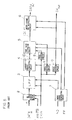
- Fig. 5 is a block diagram of a conventional audio signal demodulating circuit
- Fig. 6 is a timing chart of an audio signal in the circuit
- Fig. 7 is a MUSE transmission signal format.
- numeral 2 is an input changing circuit for changing the gain of an input data signal depending on whether the input data signal is in an AM mode or an FM mode.
- Numeral 3 is an audio low pass filter (LPF) circuit for producing an audio data signal upon receipt of an output signal of the input changing circuit 2.
- Numeral 4 is a ternary-to-binary converting circuit for converting an audio data signal output from the LPF circuit, which is a ternary two symbol audio data signal, into a binary three symbol audio data signal.
- Numeral 5 is a time-base extension circuit for receiving an audio data signal multiplexed during vertical blanking periods of a video signal and extending the time base of the received audio data signal to restore it to a continuous audio signal.
- Numeral 6 is an inter-frame de-interleave circuit for canceling the inter-frame de-interleave applied to an audio data signal at the transmission side.
- Numeral 7 is a timing signal generating circuit for producing several kinds of timing signals on the basis of a frame pulse (FP) and a horizontal pulse (HD) supplied from an image synchronization circuit (not shown).
- Numerals 8, 9 and 10 are frequency division circuits for frequency-dividing an input clock.
- an n-bit input audio data signal supplied to a data input terminal is changed in its gain corresponding to its mode by the input changing circuit 2, since the multiplexing level of an audio data signal differs between the AM mode and the FM mode, and the data signal, which has thus been changed to have an audio multiplexing level common to the AM mode and the FM mode, is supplied to the LPF circuit 3.
- the LPF circuit 3 constitutes a digital LPF circuit having a 6 MHz root cosine roll-off characteristic which serves as an audio low pass filter.
- the ternary-to-binary converting circuit 4 converts the audio data signal from a ternary two symbol signal into a binary three symbol signal.
- an audio signal has been time-multiplexed during the vertical blanking periods of a video signal, as illustrated in the MUSE transmission signal format shown in Fig. 7, to have a time-base arrangement shown at (E) of Fig. 6.
- the time-base extension circuit 5 extracts this time-multiplexed audio signal and extends its time base to provide a continuous audio signal as shown at (D) of Fig. 6.
- the inter-frame de-interleave circuit 6 operates to cancel the inter-frame interleave at the receiving side.
- a continuous audio signal is outputted from a data output terminal as an output data.
- FP frame pulse
- HD horizontal pulse
- a conventional audio signal demodulating circuit of the above construction comprises many components operating at a higher clock frequency (16.2 MHz), so that it consumes undesired excessive electrical power.
- An object of the present invention is to provide an audio signal demodulating circuit which can reduce electrical power consumption.
- the audio signal demodulating circuit according to the present invention attains this object.
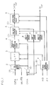
- Fig. 1 is a block diagram showing the audio signal demodulating circuit according to an embodiment of the present invention.
- Fig. 2 is a timing chart for signals appearing in the audio signal demodulating circuit.
- numeral 2 is an input changing circuit
- numeral 3 is an LPF circuit
- numeral 4 is a ternary-to-binary converting circuit
- numeral 5 is a time-base extension circuit
- numeral 6 is an inter-frame de-interleave circuit
- numeral 7 is a timing generating circuit.
- an input data signal shown at (A) of Fig. 2 is applied to the input changing circuit 2, whose gain is changed in accordance with the AM mode and the FM mode having different audio signal multiplexing levels, so that the audio signal multiplexing levels may be made equal to each other.
- the audio signal thus changed passes through a low-pass filter for audio signals having a 6 MHz root cosine roll-off characteristic.
- the audio signal is converted from a ternary two symbol signal into a binary three symbol signal through the ternary-to-binary converting circuit 4.
- timing signals synchronized with a video signal are generated through the timing generating circuit 7 on the basis of a frame pulse (FP) and a horizontal pulse (HD) supplied from a video synchronization circuit (not shown).
- One of the timing signals is a pulse such as shown at Fig. 2(B) which is synchronized with the period of the audio signal.
- the logic circuit 1 fixes the clocks to a low (or high) level as shown in Fig. 2(E) during a time period for processing signals other than an audio signal.
- the resultant clocks are used as a clock signal for the input changing circuit 2, the LPF circuit 3 and the ternary-to-binary converting circuit 4. Therefore, the output from the ternary-to-binary converting circuit 4 is substantially fixed to the low (or high) level during the period other than the audio signal period, as shown at Fig. 2(C).
- the time-base extension circuit 5 extracts the audio signal, which has been time-multiplexed during a video vertical blanking period, and extends its time-base to -form a continuous audio signal as shown at Fig. 2(D).
- inter-frame de-interleave circuit 6 cancels the inter-frame interleave applied to the audio signal at the transmission side to produce an output data.
- the logic circuit 1 is provided to fix the clock signal to a low (or high) level during the period other than the audio signal period, so that the clock signal and the input data signal are fixed during the period other than the audio signal period, thereby greatly reducing electric power consumption.
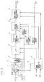
- Figs. 3 and 4 show the second embodiment of the present invention.
- the timing generating circuit 7 generates a timing signal such as shown at Fig. 4(B) which is synchronized with the period of the audio signal.
- a logic circuit 1′ operates to fix only MSB of the n-bits signal during the period other than the audio signal period to a high level and the remaining (n-l)-bits to a low level as shown at Fig. 4(C).
- the level of the signal during the period other than the audio signal period is fixed, so that electric power consumption can be reduced.
- a logic circuit which uses a timing signal generated in the timing generating circuit in synchronism with a video signal so as to fix the clock signal or input data signal to be supplied to the circuits, which process a signal before it is subjected to time-base extension, to a high level or a low level.
- the clock signal or input data signal during the period other than the audio signal period can be fixed to a high level or a low level, so that electric power consumption of the entire audio signal demodulating circuit can be remarkably reduced.
Landscapes
- Engineering & Computer Science (AREA)
- Multimedia (AREA)
- Signal Processing (AREA)
- Television Receiver Circuits (AREA)
- Television Systems (AREA)
- Circuits Of Receivers In General (AREA)
Abstract
Description
- The present invention relates to an audio signal demodulating circuit for demodulating an audio signal from a high definition television signal (MUSE signal).
- In recent years, high definition television ("high vision"), which provides more impression and deeper presence feeling and higher audio quality than convention television, has been developed. The MUSE system proposed by NIHON HOSO KYOKAI (NHK) is an example of the associated transmission system. The MUSE system is described in more detail in the NHK Technical Research Report (SHO-62), Vol. 39, No. 2, Consecutive Volume Number 172, Development of MUSE system, Pages 18-53. In the MUSE system, an audio signal is time-division multiplexed during a video V-blanking period.
- Referring now to the drawings, an explanation will be given of a circuit for demodulating an audio signal in the MUSE system.
- Fig. 5 is a block diagram of a conventional audio signal demodulating circuit, Fig. 6 is a timing chart of an audio signal in the circuit, and Fig. 7 is a MUSE transmission signal format.
- In Fig. 5,
numeral 2 is an input changing circuit for changing the gain of an input data signal depending on whether the input data signal is in an AM mode or an FM mode. -
Numeral 3 is an audio low pass filter (LPF) circuit for producing an audio data signal upon receipt of an output signal of theinput changing circuit 2.Numeral 4 is a ternary-to-binary converting circuit for converting an audio data signal output from the LPF circuit, which is a ternary two symbol audio data signal, into a binary three symbol audio data signal.Numeral 5 is a time-base extension circuit for receiving an audio data signal multiplexed during vertical blanking periods of a video signal and extending the time base of the received audio data signal to restore it to a continuous audio signal.Numeral 6 is an inter-frame de-interleave circuit for canceling the inter-frame de-interleave applied to an audio data signal at the transmission side.Numeral 7 is a timing signal generating circuit for producing several kinds of timing signals on the basis of a frame pulse (FP) and a horizontal pulse (HD) supplied from an image synchronization circuit (not shown).Numerals - The operation of the audio signal demodulating circuit as constructed above will be explained below.
- First, an n-bit input audio data signal supplied to a data input terminal is changed in its gain corresponding to its mode by the
input changing circuit 2, since the multiplexing level of an audio data signal differs between the AM mode and the FM mode, and the data signal, which has thus been changed to have an audio multiplexing level common to the AM mode and the FM mode, is supplied to theLPF circuit 3. TheLPF circuit 3 constitutes a digital LPF circuit having a 6 MHz root cosine roll-off characteristic which serves as an audio low pass filter. The ternary-to-binary converting circuit 4 converts the audio data signal from a ternary two symbol signal into a binary three symbol signal. In this case, an audio signal has been time-multiplexed during the vertical blanking periods of a video signal, as illustrated in the MUSE transmission signal format shown in Fig. 7, to have a time-base arrangement shown at (E) of Fig. 6. The time-base extension circuit 5 extracts this time-multiplexed audio signal and extends its time base to provide a continuous audio signal as shown at (D) of Fig. 6. - Then, since the input audio signal has been previously inter-frame interleaved at the transmission side in order to disperse a possible burst error occurring in the transmission system, the
inter-frame de-interleave circuit 6 operates to cancel the inter-frame interleave at the receiving side. Thus, a continuous audio signal is outputted from a data output terminal as an output data. - Additionally, the timing
signal generating circuit 7 generates and supplies several kinds of timing signals synchronized with frames of a video signal, such as used for extracting an audio signal in the time-base extension circuit 5, on the basis of a frame pulse (FP) and a horizontal pulse (HD) supplied from the video synchronization circuit (not shown). Further, thefrequency division circuits - However, a conventional audio signal demodulating circuit of the above construction comprises many components operating at a higher clock frequency (16.2 MHz), so that it consumes undesired excessive electrical power.
- An object of the present invention is to provide an audio signal demodulating circuit which can reduce electrical power consumption.
- The audio signal demodulating circuit according to the present invention, and as defined by
Claim 1, attains this object. -
- Fig. 1 is a block diagram showing the audio signal demodulating circuit according to an embodiment of the present invention;
- Fig. 2 is a timing chart for signals appearing in the audio signal demodulating circuit shown in Fig. 1;
- Fig. 3 is a block diagram showing the audio signal demodulating circuit according to another embodiment of the present invention;
- Fig. 4 is a timing chart for signals appearing in the audio signal demodulating circuit shown in Fig. 3;
- Fig. 5 is a block diagram showing a conventional audio signal demodulating circuit;
- Fig. 6 is a timing chart for an audio signal appearing in the audio signal demodulating circuit shown i Fig. 5; and
- Fig. 7 is a drawing showing a MUSE transmission signal format.
- Now referring to the drawings, an explanation will be given of an audio signal demodulating circuit according to one embodiment of the present invention. Fig. 1 is a block diagram showing the audio signal demodulating circuit according to an embodiment of the present invention. Fig. 2 is a timing chart for signals appearing in the audio signal demodulating circuit.
- In Fig. 1,
numeral 2 is an input changing circuit;numeral 3 is an LPF circuit;numeral 4 is a ternary-to-binary converting circuit;numeral 5 is a time-base extension circuit;numeral 6 is an inter-frame de-interleave circuit; andnumeral 7 is a timing generating circuit. These constituent circuits are identical to those of the conventional audio signal demodulating circuit. The audio signal demodulating circuit according to the present invention is characterized by the provision of alogic circuit 1 for fixing a clock signal to a low level during a time period for processing a signal other than an audio signal by using an output signal from the timing generating circuit. - In the above arrangement, an input data signal shown at (A) of Fig. 2 is applied to the
input changing circuit 2, whose gain is changed in accordance with the AM mode and the FM mode having different audio signal multiplexing levels, so that the audio signal multiplexing levels may be made equal to each other. Then, in theLPF circuit 3, the audio signal thus changed passes through a low-pass filter for audio signals having a 6 MHz root cosine roll-off characteristic. Then, the audio signal is converted from a ternary two symbol signal into a binary three symbol signal through the ternary-to-binary converting circuit 4. - On the other hand, several kinds of timing signals synchronized with a video signal are generated through the
timing generating circuit 7 on the basis of a frame pulse (FP) and a horizontal pulse (HD) supplied from a video synchronization circuit (not shown). One of the timing signals is a pulse such as shown at Fig. 2(B) which is synchronized with the period of the audio signal. By using this timing signal such as shown at Fig. 2(E), thelogic circuit 1 fixes the clocks to a low (or high) level as shown in Fig. 2(E) during a time period for processing signals other than an audio signal. The resultant clocks are used as a clock signal for theinput changing circuit 2, theLPF circuit 3 and the ternary-to-binary converting circuit 4. Therefore, the output from the ternary-to-binary converting circuit 4 is substantially fixed to the low (or high) level during the period other than the audio signal period, as shown at Fig. 2(C). - The time-
base extension circuit 5 extracts the audio signal, which has been time-multiplexed during a video vertical blanking period, and extends its time-base to -form a continuous audio signal as shown at Fig. 2(D). - Further, the
inter-frame de-interleave circuit 6 cancels the inter-frame interleave applied to the audio signal at the transmission side to produce an output data. - Additionally, the
frequency division circuits base extension circuit 5 and the inter-frame de-interleavecircuit 6. - In accordance with the present invention, the
logic circuit 1 is provided to fix the clock signal to a low (or high) level during the period other than the audio signal period, so that the clock signal and the input data signal are fixed during the period other than the audio signal period, thereby greatly reducing electric power consumption. - Figs. 3 and 4 show the second embodiment of the present invention. In this embodiment, the
timing generating circuit 7 generates a timing signal such as shown at Fig. 4(B) which is synchronized with the period of the audio signal. By using this timing pulse signal, alogic circuit 1′ operates to fix only MSB of the n-bits signal during the period other than the audio signal period to a high level and the remaining (n-l)-bits to a low level as shown at Fig. 4(C). Thus, in this embodiment, the level of the signal during the period other than the audio signal period is fixed, so that electric power consumption can be reduced. - In accordance with the present invention, a logic circuit is provided which uses a timing signal generated in the timing generating circuit in synchronism with a video signal so as to fix the clock signal or input data signal to be supplied to the circuits, which process a signal before it is subjected to time-base extension, to a high level or a low level. Thus, the clock signal or input data signal during the period other than the audio signal period can be fixed to a high level or a low level, so that electric power consumption of the entire audio signal demodulating circuit can be remarkably reduced.
Claims (3)
- A demodulating circuit for a MUSE television signal, the circuit including:
a gain changing circuit (2) having a signal input for receiving the MUSE signal, and a gain which depends on whether an audio signal, in the MUSE signal, is in an AM or FM mode;
an audio low pass filter (3) for receiving the output of the gain changing circuit (2);
a ternary-to-binary converting circuit (4) for converting the output of the audio low pass filter (3) from a ternary two symbol signal to a binary three symbol signal, the output of said converting circuit (4) being in the form of time multiplexed audio signals;
a time-base extension circuit (5) for extending the time base of the time multiplexed audio signals so as to provide a continuous audio signal;
an inter-frame de-interleave circuit (6) for cancelling an inter-frame interleave in the continuous audio signal;
a clock pulse input for external clock pulses;
a timing signal generating circuit (7) for generating a plurality of timing signals in response to frame and horizontal pulses in the MUSE signal; and
frequency division circuits (8,9,10) for frequency dividing the external clock pulse input,
the components of the demodulating circuit, which includes said gain changing circuit (2), said audio low pass filter (3), said ternary-to-binary converting circuit (4), said time-base extension circuit (5) and said inter-frame de-interleave circuit (6), being controlled by said clock pulse input, said timing signals and said frequency divided clock pulse input,
characterised in that the demodulator circuit further includes a logic circuit (1), which receives one of said timing signals, and which generates a high or low level signal which inhibits high frequency operation of said components, during periods other than when the time-multiplexed audio signals are output from said ternary-to-binary converting circuit (4) so as to reduce power consumption of said components in said periods. - A circuit according to Claim 1, wherein the logic circuit (1) and the frequency division circuits (8,9,10) receive said clock input, and wherein an output of the logic circuit (1) is supplied to said gain changing circuit (2), said low pass filter (3) and said ternary-to-binary converting circuit (4).
- A circuit according to Claim 1 wherein the logic circuit is connected to the input of said gain changing circuit (2).
Applications Claiming Priority (3)
| Application Number | Priority Date | Filing Date | Title |
|---|---|---|---|
| JP267453/88 | 1988-10-24 | ||
| JP63267453A JP2635388B2 (en) | 1988-10-24 | 1988-10-24 | Audio signal demodulation circuit |
| PCT/JP1989/001087 WO1990004901A1 (en) | 1988-10-24 | 1989-10-24 | Voice signal demodulation circuit |
Publications (3)
| Publication Number | Publication Date |
|---|---|
| EP0394490A1 EP0394490A1 (en) | 1990-10-31 |
| EP0394490A4 EP0394490A4 (en) | 1991-04-03 |
| EP0394490B1 true EP0394490B1 (en) | 1994-12-14 |
Family
ID=17445057
Family Applications (1)
| Application Number | Title | Priority Date | Filing Date |
|---|---|---|---|
| EP89911612A Expired - Lifetime EP0394490B1 (en) | 1988-10-24 | 1989-10-24 | Audio signal demodulation circuit |
Country Status (6)
| Country | Link |
|---|---|
| US (1) | US5121212A (en) |
| EP (1) | EP0394490B1 (en) |
| JP (1) | JP2635388B2 (en) |
| KR (1) | KR930004802B1 (en) |
| DE (1) | DE68920029T2 (en) |
| WO (1) | WO1990004901A1 (en) |
Families Citing this family (3)
| Publication number | Priority date | Publication date | Assignee | Title |
|---|---|---|---|---|
| CA2128835C (en) * | 1993-08-03 | 1999-04-06 | Daniel F. Daly | Modular digital recording logger |
| JPH08205105A (en) * | 1995-01-26 | 1996-08-09 | Hitachi Denshi Ltd | Digital signal transmission system |
| US6631606B2 (en) * | 2000-01-18 | 2003-10-14 | Dell Products L.P. | System and method for accommodating atypical customer requirements in a mass customization manufacturing facility |
Family Cites Families (5)
| Publication number | Priority date | Publication date | Assignee | Title |
|---|---|---|---|---|
| JPH0799871B2 (en) * | 1985-07-10 | 1995-10-25 | 日本電気ホームエレクトロニクス株式会社 | MUSE audio demodulator |
| JPH0750928B2 (en) * | 1985-07-10 | 1995-05-31 | 日本電気ホームエレクトロニクス株式会社 | MUSE audio information modulator |
| US4821097A (en) * | 1987-03-05 | 1989-04-11 | General Instrument Corporation | Apparatus and method for providing digital audio on the sound carrier of a standard television signal |
| KR930002640A (en) * | 1991-07-03 | 1993-02-23 | 정해영 | Scroll fluid gas |
| JPH06213177A (en) * | 1993-01-13 | 1994-08-02 | Kobe Steel Ltd | Scroll compressor |
-
1988
- 1988-10-24 JP JP63267453A patent/JP2635388B2/en not_active Expired - Fee Related
-
1989
- 1989-10-24 KR KR1019900701320A patent/KR930004802B1/en not_active Expired - Fee Related
- 1989-10-24 DE DE68920029T patent/DE68920029T2/en not_active Expired - Fee Related
- 1989-10-24 EP EP89911612A patent/EP0394490B1/en not_active Expired - Lifetime
- 1989-10-24 US US07/499,353 patent/US5121212A/en not_active Expired - Lifetime
- 1989-10-24 WO PCT/JP1989/001087 patent/WO1990004901A1/en not_active Ceased
Also Published As
| Publication number | Publication date |
|---|---|
| EP0394490A4 (en) | 1991-04-03 |
| DE68920029T2 (en) | 1995-07-20 |
| DE68920029D1 (en) | 1995-01-26 |
| US5121212A (en) | 1992-06-09 |
| EP0394490A1 (en) | 1990-10-31 |
| KR900702709A (en) | 1990-12-08 |
| WO1990004901A1 (en) | 1990-05-03 |
| JPH02113728A (en) | 1990-04-25 |
| JP2635388B2 (en) | 1997-07-30 |
| KR930004802B1 (en) | 1993-06-08 |
Similar Documents
| Publication | Publication Date | Title |
|---|---|---|
| US5550589A (en) | Method of adaptively multiplexing a plurality of video channel data using channel data assignment information obtained from a look-up table | |
| JP2625102B2 (en) | Encoder, decoder, communication method and apparatus for MAC television signal | |
| US3921204A (en) | Digital encoding system | |
| JP3369359B2 (en) | Digital high definition television signal receiver with imaginary sample presence detector for quadrature amplitude modulation / vestigial sideband mode selection | |
| EP0181189A2 (en) | Video signal processing system | |
| US4965820A (en) | Cellular telephone apparatus | |
| US4858008A (en) | Apparatus for the digital generation of vertical synchronizing and field identification signals | |
| US5121212A (en) | Audio signal demodulating circuit with reduced power consumption | |
| JP2548766B2 (en) | Compander for digital video signals | |
| EP0021132B1 (en) | Sampling clock reproducing apparatus | |
| US3825680A (en) | Receiver for video signals | |
| US5835158A (en) | Analog signal process with dither pattern | |
| US5252972A (en) | Codec having controllable frame synchronizing and clocking signals | |
| EP0543220A1 (en) | Method and apparatus for A/D and D/A conversion | |
| US4204163A (en) | Minimum group pulse code modem having shape and amplitude codes | |
| JP2783008B2 (en) | Frame synchronizer | |
| EP0341989B1 (en) | Apparatus for simultaneously outputting plural image signals derived from a video signal, comprising a single digital-to- analogue converter | |
| JP3021966B2 (en) | Synchronous signal generation circuit and video signal processing device | |
| US4977452A (en) | Sampled-value code processing device | |
| KR100213002B1 (en) | Sampling frequency conversion circuit | |
| JPS61148986A (en) | Television signal sampling device | |
| JPH0733500Y2 (en) | Television phone | |
| JPH089940Y2 (en) | Digital signal decoder | |
| JPH0349384A (en) | Video signal encoding device | |
| JPS6341471B2 (en) |
Legal Events
| Date | Code | Title | Description |
|---|---|---|---|
| PUAI | Public reference made under article 153(3) epc to a published international application that has entered the european phase |
Free format text: ORIGINAL CODE: 0009012 |
|
| 17P | Request for examination filed |
Effective date: 19900703 |
|
| AK | Designated contracting states |
Kind code of ref document: A1 Designated state(s): DE FR GB |
|
| RIN1 | Information on inventor provided before grant (corrected) |
Inventor name: OHTSUKA, YOSHIMICHI 10-10, IKUTA 6-CHOME Inventor name: ARITA, HISASHI 3-7, WAKABA 2-CHOME Inventor name: IWAMOTO, TAKUSHI Inventor name: OKUMURA, NAOJI Inventor name: NINOMIYA, YUICHI 17-4, TAKAISHI 2-CHOME Inventor name: KAWASHIMA, TADASHI |
|
| A4 | Supplementary search report drawn up and despatched |
Effective date: 19910215 |
|
| AK | Designated contracting states |
Kind code of ref document: A4 Designated state(s): DE FR GB |
|
| RAP1 | Party data changed (applicant data changed or rights of an application transferred) |
Owner name: MATSUSHITA ELECTRIC INDUSTRIAL CO., LTD. Owner name: NIPPON HOSO KYOKAI |
|
| 17Q | First examination report despatched |
Effective date: 19930503 |
|
| GRAA | (expected) grant |
Free format text: ORIGINAL CODE: 0009210 |
|
| AK | Designated contracting states |
Kind code of ref document: B1 Designated state(s): DE FR GB |
|
| REF | Corresponds to: |
Ref document number: 68920029 Country of ref document: DE Date of ref document: 19950126 |
|
| ET | Fr: translation filed | ||
| PLBE | No opposition filed within time limit |
Free format text: ORIGINAL CODE: 0009261 |
|
| STAA | Information on the status of an ep patent application or granted ep patent |
Free format text: STATUS: NO OPPOSITION FILED WITHIN TIME LIMIT |
|
| 26N | No opposition filed | ||
| REG | Reference to a national code |
Ref country code: GB Ref legal event code: IF02 |
|
| PGFP | Annual fee paid to national office [announced via postgrant information from national office to epo] |
Ref country code: FR Payment date: 20051010 Year of fee payment: 17 |
|
| PGFP | Annual fee paid to national office [announced via postgrant information from national office to epo] |
Ref country code: GB Payment date: 20051019 Year of fee payment: 17 |
|
| PGFP | Annual fee paid to national office [announced via postgrant information from national office to epo] |
Ref country code: DE Payment date: 20051020 Year of fee payment: 17 |
|
| PG25 | Lapsed in a contracting state [announced via postgrant information from national office to epo] |
Ref country code: DE Free format text: LAPSE BECAUSE OF NON-PAYMENT OF DUE FEES Effective date: 20070501 |
|
| GBPC | Gb: european patent ceased through non-payment of renewal fee |
Effective date: 20061024 |
|
| REG | Reference to a national code |
Ref country code: FR Ref legal event code: ST Effective date: 20070629 |
|
| PG25 | Lapsed in a contracting state [announced via postgrant information from national office to epo] |
Ref country code: GB Free format text: LAPSE BECAUSE OF NON-PAYMENT OF DUE FEES Effective date: 20061024 |
|
| PG25 | Lapsed in a contracting state [announced via postgrant information from national office to epo] |
Ref country code: FR Free format text: LAPSE BECAUSE OF NON-PAYMENT OF DUE FEES Effective date: 20061031 |