EP0390651B1 - Fiberoptic techniques for measuring the magnitude of local microwave fields and power - Google Patents
Fiberoptic techniques for measuring the magnitude of local microwave fields and power Download PDFInfo
- Publication number
- EP0390651B1 EP0390651B1 EP90400787A EP90400787A EP0390651B1 EP 0390651 B1 EP0390651 B1 EP 0390651B1 EP 90400787 A EP90400787 A EP 90400787A EP 90400787 A EP90400787 A EP 90400787A EP 0390651 B1 EP0390651 B1 EP 0390651B1
- Authority
- EP
- European Patent Office
- Prior art keywords
- sensor
- microwave
- optical fiber
- microwave absorbing
- further characterized
- Prior art date
- Legal status (The legal status is an assumption and is not a legal conclusion. Google has not performed a legal analysis and makes no representation as to the accuracy of the status listed.)
- Expired - Lifetime
Links
Images




Classifications
-
- G—PHYSICS
- G01—MEASURING; TESTING
- G01R—MEASURING ELECTRIC VARIABLES; MEASURING MAGNETIC VARIABLES
- G01R21/00—Arrangements for measuring electric power or power factor
- G01R21/02—Arrangements for measuring electric power or power factor by thermal methods, e.g. calorimetric
-
- G—PHYSICS
- G01—MEASURING; TESTING
- G01K—MEASURING TEMPERATURE; MEASURING QUANTITY OF HEAT; THERMALLY-SENSITIVE ELEMENTS NOT OTHERWISE PROVIDED FOR
- G01K17/00—Measuring quantity of heat
- G01K17/003—Measuring quantity of heat for measuring the power of light beams, e.g. laser beams
-
- G—PHYSICS
- G01—MEASURING; TESTING
- G01R—MEASURING ELECTRIC VARIABLES; MEASURING MAGNETIC VARIABLES
- G01R1/00—Details of instruments or arrangements of the types included in groups G01R5/00 - G01R13/00 and G01R31/00
- G01R1/02—General constructional details
- G01R1/06—Measuring leads; Measuring probes
- G01R1/067—Measuring probes
- G01R1/07—Non contact-making probes
- G01R1/071—Non contact-making probes containing electro-optic elements
-
- G—PHYSICS
- G01—MEASURING; TESTING
- G01R—MEASURING ELECTRIC VARIABLES; MEASURING MAGNETIC VARIABLES
- G01R29/00—Arrangements for measuring or indicating electric quantities not covered by groups G01R19/00 - G01R27/00
- G01R29/08—Measuring electromagnetic field characteristics
- G01R29/0864—Measuring electromagnetic field characteristics characterised by constructional or functional features
- G01R29/0878—Sensors; antennas; probes; detectors
- G01R29/0885—Sensors; antennas; probes; detectors using optical probes, e.g. electro-optical, luminescent, glow discharge, or optical interferometers
Definitions
- This invention relates generally to methods, sensors and instrumentation for measuring the strength of electromagnetic fields and power, particularly in the microwave region of the spectrum.
- electromagnetic radiation within the microwave and radio frequency ranges is being used increasingly in industry for processing various dielectric materials -- e.g., plastics, rubber, wood products and ceramics.
- the primary desired result is to produce throughout the product volume very rapid heating and thereby quick drying, curing, firing and so on.
- the primary variable under the control of the user or operator is the average applied power which in turn relates directly to the average strength of the fields present in the processing chamber.
- the incident electromagnetic waves in these and similar processes consist of time-varying E (electric) and H (magnetic) fields oriented at right angles to one another and to the direction of propagation.
- Either the E-field or H-field can produce heating but normally the E-field produces the dominant effects.
- the E-field produces oscillating current flow and thereby resistive heating if the medium is conductive.
- the E-field can also produce oscillating motion of bound charges (polarization) and reorientation of permanently polar molecules (such as water), and these effects also lead ultimately to heating.
- Interest in H-field measurements is limited primarily to the processing of magnetic materials or, occasionally, to the indirect measurement of currents induced by electromagnetic waves in processing chamber walls.
- the power available at a given point in a processing chamber is proportional to the square of the effective field, either E or H.
- the material being processed will further alter the microwave field and power distributions within the material because of the larger dielectric constant of the material relative to free space or air and the absorption of microwaves by the material. Knowledge of these effects can be further utilized to optimize the size, composition, and shape of the product and/or the speed of processing.
- a remote sensor can either be located elsewhere within the processing chamber or in a waveguide leading from the chamber to a dummy load.
- a particular problem of interest involves optimizing the design of a microwave food product utilizing "active" packaging -- i.e. packaging which either preferentially concentrates or homogenizes the microwave energy distribution incident on the food product or, in the case of metallic susceptor films, absorbs additional microwave energy locally in the film to provide preferential heating of adjacent portions of the food product (e.g., the crust of a pizza or sausage roll).
- active packaging i.e. packaging which either preferentially concentrates or homogenizes the microwave energy distribution incident on the food product or, in the case of metallic susceptor films, absorbs additional microwave energy locally in the film to provide preferential heating of adjacent portions of the food product (e.g., the crust of a pizza or sausage roll).
- a very small probe capable of measuring local fields within the package or food product would be useful in evaluating the degree to which the microwave power distribution internal to the product has been altered by the specific package design.
- a fifth reason for measuring the level of such fields pertains to computer modeling. As better computer models are developed for analyzing and eventually optimizing food product designs, good input data, including local microwave fields, will be needed for these models. Field probes will therefore be needed to provide this information internal to the product.
- Present field measurement techniques are electrical and utilize electrically-conducting antennas of various designs. These antennas have typically been developed for measuring weak fields, as for example the leakage of microwaves from a closed, operating oven. Such antennas cannot survive, let alone measure, the intense heating fields inside of an operating oven or processing chamber.
- Such leakage field monitoring antennas have been designed for the most efficient coupling to the fields being measured.
- a dipole antenna is typically designed with a length that is one-half the wavelength of the radiation being measured.
- the microwave oven operates at 245 ⁇ MHz.
- the wavelength corresponding to this frequency in free space (or air) is about 12 cm.
- a half wavelength dipole is a little over 2 inches in length.
- An orthogonal array of three crossed dipoles is normally used to provide orientation-independent measurements.
- This array is typically contained in a polystyrene foam sphere, both for protection and for insulation.
- the outer sphere then has a diameter of about 2 1/2" or greater, a size which is too large to allow detailed mapping within the oven and which would be impossible to use for measurements internal to a typical food product.
- the field measurements be made by thermal techniques, using a small, minimally-perturbing sensor designed to be heated predictably by the oscillating fields with the resultant temperature rise then being measured by passive fiberoptic techniques.
- a small, minimally-perturbing sensor designed to be heated predictably by the oscillating fields with the resultant temperature rise then being measured by passive fiberoptic techniques.
- Luxtron Corporation assignee of the present application, has perfected a phosphor-based temperature sensing technology which can be used with either remote viewing or with the phosphor sensor attached to the end of an optical fiber. By monitoring the fluorescent decay time of the phosphor, one can determine its temperature.
- EEDs electroexplosive devices
- the bridge wire of the EED is a resistive conductor whose current is raised by the high frequency induced current flowing through it.
- the temperature rise is proportional to the resistance and to the square of the induced current.
- the EED thus becomes a current sensor for detecting currents induced in the cabling of the firing circuit connected to it. Calibration of the sensor is performed by injecting known currents and noting the resultant temperature rises.
- a sensor is provided at an end of a length of optical fiber, and has two primary elements, namely: a first element adapted to be heated by either or both of the electrical field or the magnetic field components of the microwave radiation environment in which the sensor is placed, and a second element in thermal contact with the first element having at least one optical characteristic that changes as a function of its temperature and which is detectable at an opposite end of the optical fiber by an instrument provided for that purpose.
- the first element can include one or more short electrically resistive wires, in either a one-dimensional, two-dimensional or a three-dimensional arrangement, a sphere made from a resistively conductive material, or a quantity of a polar dielectric material.
- a magnetic (H) field sensor either an electrically resistive current loop, such as one provided by a sphere made from a material cf adequately high electrical conductivity, or a quantity of electrically non-conductive, magnetizable (i.e., ferrimagnetic) material is provided.
- the sensors are made to be quite small in physical size in order to make detailed field and power mapping possible.
- the sensors are intentionally made to have a poor coupling with the high power microwave fields in order that the sensors will not be damaged and the fields will not be unduly perturbed by the presence of the sensors.
- the sensors may even be imbedded in materials being heated by the microwave fields, or may be positioned outside of the material but within the chamber (such as a microwave oven) that confines the microwave energy.
- the sensors can also be used for making free field measurements of power or field strength, such as in the mapping of high power antenna beam patterns.
- an apparatus for measuring the strength of a microwave field comprising a sensor carried by one end of a length of an optical fiber communication medium, the sensor including a microwave absorbing element that becomes heated when positioned within a microwave field, and luminescent material positioned in thermal contact with the microwave absorbing element and in optical communication with one optical fiber medium end, the luminescent material, in response to receiving excitation radiation, emitting radiation that is within a visible or near-visible portion of the electromagnetic radiation spectrum and which has at least one detectable optical characteristic that is dependent upon its temperature.
- This invention is characterized by the fact that the microwave absorbing element has a symmetrical three-dimensional shape. A corresponding method is claimed in method claim 12.
- an enclosure 11 contains an item 13 in a space 15 within the enclosure 11 that is being heated by high frequency electromagnetic radiation 17.
- the radiation is generated by a power source 21 outside of the chamber which transmits electromagnetic radiation by means of a waveguide to the chamber.
- the system shown in Figure 1 is representative of the usual home microwave oven, a similar type of oven used commercially, or an industrial processing chamber where microwave energy is used to dry, fire or cure a larger quantity of material as part of an industrial process.
- the material 13 being heated is usually an item of food, while in an industrial process, the material being heated may be a food, plastic, rubber, wood product or ceramic object.
- a sensor 23 is positioned within the chamber.
- the sensor 23 is attached to one end of a length of optical fiber 25, another end of the optical fiber 25 being connected to a measuring instrument 27 that is outside of the chamber 15.
- the sensor 23 can be embedded in the material 13 being processed, or can be positioned in space anywhere within the chamber 15, depending upon the goal of the measurement that is to be made.
- the sensor 23 is built on an end 31 of the length of optical fiber 25, and includes two primary elements.
- a first such element 33 is characterized by being heated by the strong microwave field 17.
- the element 33 can be one of several specific types of microwave absorbers described hereinafter, including an electrically resistive wire or array of wires, a polar dielectric medium, a resistively conducting sphere, a quantity of ferrimagnetic material, and the like, depending upon the application and whether the electric field or magnetic field is desired to be measured.
- the sensing element 33 operates by elevating its temperature by an amount proportional to the power absorbed which in turn is proportional to the square of the field that is being measured.
- a second primary element 35 of the sensor 23 measures that temperature rise by optical means.
- the temperature sensing element 35 is placed in thermal communication with the sensing element 33, as indicated by the heat waves 37, usually by close physical contact that allows unimpeded heat conduction between them.
- a heat conductive medium is provided between them.
- the optical temperature sensing element 35 may be of any type that is characterized by exhibiting a change in at least one optical property as a function of temperature that can be detected and measured by the instrument 27 through the optical fiber 25.
- a preferred optical temperature sensing element 35 is formed from a luminescent material.
- the preferred luminescent material for the element 35 and the method used by the instrument 27 to measure temperature of that element is described in U.S. Patent No. 4,652,143 - Wickersheim et al. (1987), which is expressly incorporated herein by reference.
- a luminescent element 35 is excited to fluoresce by a pulse of exciting radiation 39 developed in the instrument 27. This is followed by a decaying pulse of fluorescent radiation 41 from the element 35. It is that rate of decay of this fluorescent light pulse that is measured by the instrument 27 as a measure of the temperature of the element 35.
- the optical temperature sensing element 35 is chosen to be of a type that is not itself heated directly by the microwave radiation. Specifically, the temperature sensing element 35 and its signal transmitting leads do not incorporate any electrically conductive materials, any strongly polar dielectric materials, or any magnetic materials. (An exception to this is where the functions of the elements 33 and 35 are performed by a single material or a composite element.)
- a separate temperature sensor made of an optical temperature sensing element 43, preferably including a luminescent material, and a second optical fiber 45 that optically communicates between the sensor 43 and the instrument 27.
- the optical temperature sensing element 43 is positioned to measure the ambient temperature of the environment in which the sensor 23 is positioned.
- the second temperature reading provides a base from which the elevated temperature measured by the optical element 35 may be determined at any instant in time. It is that temperature difference that is proportional to the energy absorbed from the incident microwave field 17, and thus to the local power, since the temperature sensor 43 is chosen to be unaffected by the field 17.
- the temperatures of each of the sensors 35 and 43 are measured by the instrument 27 discussed previously. Calculation of the local microwave power density or strength can be accomplished by a personal computer (not shown) connected to the instrument 27 used to determine the two temperatures. A difference between the two temperatures is first calculated, and that difference is then used to calculate the microwave quantity being measured according to an empirically determined calibration inputed into computer memory. If it is desired to provide an instrument that is dedicated to such microwave measurements, the optical temperature measuring and computer functions can be integrated into a single device.
- the various aspects of the present invention can be applied to a number of specific microwave frequencies, and even to electromagnetic frequencies in radio frequency ranges outside of the microwave spectrum.
- Home and industrial microwave ovens usually operate at about 2450 MHz., a frequency allocated for industrial, scientific and medical use by the Federal Communications Commission of the United States government.
- Other commonly used frequencies allocated for that purpose are at approximately 13, 27 and 915 MHz.
- Most industrial, scientific and medical microwave heating systems operate within these allocated frequency ranges, since to operate at other frequencies would require the use of heavily shielded rooms to contain any strong radiation.
- microwave sensing techniques of the present invention is to measure the strength of microwave fields produced by radar or communications equipment, medical hyperthermia equipment, military electromagnetic radiation testing facilities, and any other application where strong electromagnetic radiation within or near the microwave frequency range is being utilized.
- the small size and easy positioning of the sensors being described herein make them especially convenient to measure the power of field distribution across a microwave field.
- An example is to measure the profile of a microwave antenna beam pattern. A profile can be obtained by either taking a plurality of measurements across a beam with a single sensor or by simultaneously using a plurality of sensors positioned across the beam.
- the microwave frequency range is considered to extend from about 300 MHz. to 300 GHz.
- the sensors being described are specially adapted for use in high power microwave environments, such as occur inside a microwave oven or directly in the path of a microwave beam from a transmitter, and are not specifically designed for detecting low level radiation, such as may be found to be leaking from such devices.
- Other, more conventional techniques are better suited for measuring low-level, leakage radiation.
- FIG 3 illustrates a sensor for measuring the intensity of the electric field component of microwave radiation.
- a cylindrically shaped housing 47 is provided.
- the housing 47 has a cylindrically shaped bore 49 in one end thereof.
- an optical fiber 51 extends along the axis of the cylinder of the housing 47, into the bore 49 and terminating at a position 53.
- the radiation sensing element corresponding to element 33 of Figure 2 is a short piece of electrically resistive wire 55.
- the wire 55 extends between the inner walls of the bore 49 and is attached thereto at its ends 57 and 59. In about the middle of the length of the wire 55 is attached a layer or quantity 61 of luminescent material that corresponds to the optical temperature sensing element 35 of Figure 2.
- the housing 47 is made from a plastic material that is neither electrically nor thermally conductive.
- the wire sensor 55 is of small diameter and is preferably made of a resistively conducting metal such as tungsten wire of the type used in electric light bulbs, or of nichrome or of other resistive fibers such as carbon-loaded plastic.
- the wire sensor 55 is electrically isolated from its surroundings. The only part of the sensor of Figure 3 that interacts with the microwave radiation field in which it is placed is the short piece of wire 55.
- the fiber end 53 is spaced a short distance away from the luminescent material 61.
- the air gap between the fiber and the luminescent material 61 provides a thermally insulative layer.
- the luminescent material 61 is, of course, attached to the wire 55 in a manner to maximize the thermal conductivity between the two.
- the housing 47 protects the wire sensor somewhat from the effects of air currents of varying temperatures that might exist where the sensor is being used.
- the open end of the bore 49 further may be sealed (not shown) to form an enclosed cavity filled with air, thereby to make it even more insensitive to air currents of varying temperatures. Such sealing also allows the sensor to be immersed in liquids without liquid contacting the sensor elements.
- the length of the wire 55 is chosen to be small relative to the wavelength of the microwave field being measured.
- the wavelength in air of the popular 2450 MHz. frequency used in microwave cooking is about 12 centimeters, and for 915 MHz. about 32 centimeters.
- a usual microwave field measuring technique utilizing a resonant antenna requires the antenna to be one-half wavelength long, or about six centimeters in length, to measure a 2450 MHz. field.
- the length of the wire 55 is intentionally chosen to be significantly non-resonant with the microwave field being measured.
- the length of the wire 55 is typically made to be less than two centimeters, and preferably less than one centimeter.
- An advantage of using a thin wire sensor as illustrated in Figure 3 is that it has very little thermal mass and thus will be heated quite rapidly by the electric field component of the microwave radiation in which it is placed as shown in Figure 13A. It will also cool rapidly when removed from that radiation field, thus providing a quick response to changing radiation levels or to movement of the sensor within a microwave radiation field that is not uniform.
- the sensor does not perturb the radiation field significantly since it is very weakly coupled with it by being of a length far from that which would be resonant with the microwave radiation being measured.
- the sensor of Figure 3 is obviously quite directional. That is, the measured temperature rise of the wire sensor 55 is dependent in part upon the orientation of its length with respect to the electric field of the microwave radiation.
- a highly directional sensor is desired.
- Such a non-directional (isotropic) field sensor can be made by using a plurality of short wires, instead of one, and orienting them in a symmetric three-dimensional pattern.
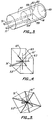
- An example of this is shown in Figure 4 where three lengths of wire 63, 65 and 67 are oriented substantially orthogonally to each other and joined at their mid-points where the luminescent sensing material 61′ is attached.
- the ends of the three wires 63, 65 and 67 are attached to the cylindrical sensor housing 47, in this example of a modification of what is shown in Figure 3.
- Each of the wires 63, 65 and 67 is made to have the same length and characteristics as the single wire 55 as described with respect to that embodiment.
- the imaginary cube in Figure 4 is intended to illustrate the symmetric orientation of the wires with respect to each other and with respect to the communicating optical fiber 51′.
- Each end of the wires 63, 65 and 67 is terminated at a mid-point of a different side of that cube.
- the optical fiber 51′ extends from a corner of that cube to position its end 53′ a short distance from the luminescent temperature sensor 61′.
- the heating of the luminescent sensor 61 is substantially the same no matter what the orientation of this modified sensor illustrated in Figure 4 with respect to the microwave field in which it is placed.
- Figure 5 illustrates yet another modification of the sensor of Figure 3 where four lengths of resistive wire are joined together at their mid-points where the luminescent sensor 61 ⁇ is attached.
- Each of the lengths of wires extends between opposite corners of an imaginary cube shown in Figure 5, while the fiber 51 ⁇ enters the cube through a mid-point in one face thereof so that its end 53 ⁇ is positioned a short distance away from the luminescent material sensor 61 ⁇ .
- the length of each of the individual wires, material, and so forth, are similar to that described for the individual wire 55 of Figure 3.
- a second luminescent sensor 69 is attached to a second optical fiber 71 that is carried by the cylindrical housing 47 ( Figure 3).
- the sensor 69 is of a standard commercial type, being designed to measure the temperature of the environment in which it is immersed.
- the sensor 69 is positioned far enough away from the wire 55 so that it measures principally the temperature of the air adjacent to the heated wires.
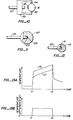
- Curves of Figure 13A show the results of an electric field measurement with the sensor of Figure 3, modified to include the three crossed wires of Figure 4.
- a curve 115 shows the variation in temperature of the sensor 61′ during application of a microwave power pulse.
- a microwave field of constant magnitude is turned on at a time t1 and turned off at a time t2.
- a curve 117 shows the temperature variation of the reference sensor 69 during the same time interval.
- the temperature of the reference sensor 69 increases during the t1-t2 interval as a result of the air within the cavity 49 of the sensor being heated by the wire sensors.
- a difference in the temperature measured by the two sensors 61′ and 69 remains substantially constant during the interval when the microwave power is turned on, as indicated by the curve of Figure 13B. It is this temperature difference which is proportional to the microwave power lever in the environment in which the sensor is positioned.
- the housing 47 may be omitted.
- the wire(s) are made to be self supporting by selection of the wire material and diameter. Silicon carbide fiber is satisfactory.
- the wire structure is supported by attachment to its associated optical fiber end at the location of the luminescent material.
- this modification would cause the wires 63, 65 and 67 to be attached to the optical fiber end 53′ at the point where they are attached to each other and carry the luminescent material 61′.
- This modified structure has the advantage that any adverse thermal or dielectric effects of the housing 47 on a desired isotropic characteristic of the sensor are eliminated.
- the advantages of the housing 47 discussed above are not, of course, present in such an arrangement.
- sensors illustrated in Figures 6, 7 and 8 contain no electrically conductive element in order to measure the electric field component of microwave radiation. Rather than heating an electrically resistive element, the oscillating electric field in these sensor embodiments causes heating by inducing molecular rotation of highly polar molecules in a dielectric medium.
- a luminescent or other optical temperature sensor 73 is attached to an end of an optical fiber 75.
- a cap 76 holds a quantity of the polar dielectric material 77 immediately adjacent the temperature sensor 73. It is the material 77 that becomes heated an amount proportional to the square of the electric field in which it is placed. Water molecules are useful for this purpose since they have a permanent electric dipole moment.
- Water molecules are therefore caused to rotate by an oscillating electric field, thus causing heating.
- very little water is required for use in high power fields and so must be diluted with a non-polar dielectric material in many cases. It may be diluted by mixing a small amount of water into a gel or paste. Because of the semi-liquid form of such a sensor 77, containment may be required, as by the cap 76, in order to provide physical stability and to reduce evaporative losses.
- a water-based sensor 77 might include a stable hydrated crystal, such as gypsum, or water adsorbed on silica gel. Polarizable materials not having a permanent dipole moment may also be utilized, although the heating effects would be much weaker.
- the sensor of Figure 6 has an advantage over the wire sensor embodiments of Figures 3-5 because of its smaller size and since it operates by virtue of bulk absorption and is thus inherently more isotropic.
- Figure 7 shows a sensor that is a modified version of that of Figure 6.
- particles of the optical sensor are dispersed, in the embodiment of Figure 7, throughout the volume of the dielectric 77. This is appropriate where the dielectric 77 is substantially optically transparent, and results in better thermal contact between the dielectric element, whose temperature rise is being measured, and the optical material that is measuring that rise. It is particularly convenient when the optical sensor is a phosphor since particles of such a material can easily be formed and dispersed in the dielectric volume.
- FIG. 8 Another form of a dielectric electric field measuring probe is shown in Figure 8 wherein a volume 81 of a polar solid material is formed directly on the end of an optical fiber 83.
- a volume 81 of a polar solid material is formed directly on the end of an optical fiber 83.
- An example of such a material is Nylon 66. If the material is substantially optically transparent, particles of luminescent material, as the optical temperature sensor, can be dispersed in it, as shown in Figure 8. Alternatively, if the material is not transparent enough, the luminescent layer may be attached directly to the end of the optical fiber 83 but in thermal contact with the dielectric material 81.
- Figure 9 shows a sensor configuration that can be used to measure the level of the magnetic field.
- a layer 85 of electrically resistive material is carried by an end of an optical fiber 87.
- a significant amount of surface area of the layer 85 is provided.
- surface be formed in a spherical shape, as shown in Figure 9.
- the level of resistivity and size of the sensor determines its responsiveness to the electric or magnetic field components.
- Other elements of the sensor include a luminescent material layer 86 also attached to an end of the optical fiber 87.
- a hard, transparent epoxy "ball” 89 surrounds the end of the fiber and supports the luminescent layer 86 and the magnetic field sensing electrically resistive overcoating 85.
- the diameter of the epoxy ball 89 is made large enough, typically 1 to 2 millimeters in diameter, to provide the necessary amount of surface area in order to result in a high enough temperature rise from the field being measured to allow accurate measurement.
- Material suitable for the layer 85 includes carbon or silver-loaded epoxy.
- the sensor of Figure 9 operates as a small current loop.
- the conductivity of the spherical surface 85 is high enough that it absorbs magnetic radiation, the oscillating H field being measured penetrates the resistive spherical surface and generates currents in the resistive layer in a plane at right angles to the field vector. These currents cause Joule heating in the resistive surface layer and the optical temperature sensor detects this heating.
- an isotropic field sensor is shown in Figure 10, wherein a ball 91 is coated with an electrically resistive material like that of the layer 85 of the embodiment of Figure 9.
- the ball 91 is held displaced a short distance from an end of the optical fiber 93 by thermally insulative support elements 94 and 96 carried by a primary support member 95.
- the optical temperature sensor is in the form of a luminescent layer 97 deposited on top of, and thus in thermal contact with, the electrically resistive layer that heats up in the electromagnetic field.
- This embodiment although somewhat more complicated than that of Figure 9, has an advantage of providing an air gap between the heated electrically resistive material layer and the optical fiber, thus reducing heat conduction by the optical fiber away from the region being measured.
- the portions 94 and 96 are preferably thin glass or plastic fiber filaments.
- Figure 11 illustrates another form of magnetic field sensor.
- An optical fiber 101 has a hard hemispherical ball 103 of substantially optically clear epoxy attached to an end thereof. Surrounding this hemisphere is a layer 105 of temperature sensing luminescent material. Further, surrounding the temperature sensing layer 105 and the hemisphere 103, is another, larger sphere 107.
- the sphere 107 contains particles, as shown, of electrically conductive material. Material suitable for the particles within the sphere 107 are silver or carbon.
- an optical fiber 109 includes a luminescent temperature sensing layer 111 attached to its end. Surrounding the luminescent layer 111 is a solid quantity 113 of a ferrimagnetic material.
- a microwave ferrite or yttrium iron garnet Surrounding the luminescent layer 111 is a solid quantity 113 of a ferrimagnetic material.
- An example of such a material is a microwave ferrite or yttrium iron garnet. This material is characterized by being electrically non-conducting but magnetizable. It is the magnetic equivalent, for the purposes of measuring a varying magnetic field component of microwave radiation, of the dielectric sensor described earlier for the purpose of measuring the electrical field component.
- a further embodiment of a ferrimagnetic material sensor employs the configuration described above with respect to Figure 10. But in this case, the sphere 91 is made of solid ferrimagnetic material and the luminescent layer 97 is coated over a portion of its surface.
- FIG. 14C a technique for making another sensor having a spherically shaped electrically conductive shell is illustrated by sectional views taken through approximately the center of the spherical elements.
- Figure 14C shows the completed sensor formed at an end of an optical fiber 121.
- An optical temperature sensor 123 is attached to an end portion 125 of the optical fiber wherein its outer protective sheath has been removed.
- a thin spherical element that becomes heated in an electromagnetic field by absorption of either its electric or magnetic field component, or both, is physically carried by the optical fiber 121 with the temperature sensor 123 in thermal communication with the sphere 127 by physical contact with an inside surface of the sphere.
- the physical arrangement of the sensor of this embodiment differs from that of Figure 9 primarily by the positioning of the optical temperature sensing material.
- an interior region 129 is hollow rather than being filled with a supporting ball 89 of the Figure 9 embodiment.
- a first step in making the sensor of Figure 14C is to push the optical fiber end 121 though a spherical bead 131 of polystyrene foam, the material used in making popular thermal insulative coffee cups.
- the bead outside diameter is small, such as approximately 2 mm., and allows penetration of the optical fiber end portion 125, typically about 0.4 mm. in diameter.
- the optical fiber 121 is pushed far enough into the bead 131 from one side until its temperature sensor 123 just begins to emerge from an opposite side.
- the assembly of Figure 14A is then dipped into a liquid mixture to form the shell 127 shown in Figure 14B.
- this liquid is a slurry mixture of tin oxide as the active electromagnetic sensing material and a water based binder such as potassium silicate.
- the resulting coated bead 131 of Figure 14B is then heated to a maximum of 200 degrees centigrade, resulting in the structure shown in Figure 14C.
- the heating step dries the coating on the bead 131 to form a hard shell 127.
- a shell thickness of about 0.2 mm. is desireable.
- the polystyrene bead 131 is melted by the heating step and, upon cooling, leaves a much smaller bead 133 attached to a surface inside the shell 127, usually on the optical fiber portion 125. Because the polystyrene sphere 131 is mostly air, its size reduction is dramatic when it melts.
- the resulting hollow sensor 134 of Figure 14C has a very low amount of thermal mass and thus provides a quick response to measure the strength of an electromagnetic field in which the sensor is positioned.
- a main advantage of a spherically shaped sensor is that it is quite insensitive to its orientation within (i.e., is isotropic with respect to) the electromagnetic field being measured, regardless of whether the sensor is more responsive to the electric or magnetic component of that field. Isotropy is usually desired but such sensors can be formed in other shapes when a directional sensitivity is needed for a special application.
- the method of Figures 14A-14C can certainly be used to form the shell 127 in other enclosed shapes by starting with the polystyrene bead 131 in a different shape.
- the degree to which the sensor 134 responds to the electric or magnetic components of a microwave field is determined primarily by the level of electrical conductivity (or, inversely, resistivity) of the shell 127 and its diameter relative to the wavelength of the electromagnetic field being measured. As the conductivity is increased for a given size shell, the percentage of the magnetic field component absorbed by the shell 127 goes up while the percentage of the electric field component absorbed goes down. If the conductivity is decreased, the reverse occurs.
- the tin oxide shell 127 of this specific example makes a sensor 134 that is predominately an electric field sensor.
- a sensor of the type shown in Figure 9 may be made with a substantially hollow region in its middle instead of the epoxy ball 89.
- the polystyrene bead 131 is first coated with a temperature sensing luminescent material layer that becomes the layer 86 ( Figure 9), and then is coated with an electromagnetic field heating layer, as described above, that becomes the layer 85 ( Figure 9). Heating of the polystyrene bead, now coated with two layers, leaves a modified Figure 9 sensor having low thermal mass and in which optical signals communicate between the luminescent material layer 86 and an end of the optical fiber 87 through a void.
- the sensor 134 of Figure 14C can be used alone but it is generally preferable to provide such a sensor as part of a structure that also incorporates a reference temperature sensor in order to make a differential temperature measurement, as previously discussed.
- a composite sensor is shown in a cross-sectional view of Figure 15.
- a thin walled cylindrical envelope 135 is shaped to close off one end 136 and receives a plug 137 at an opposite end.
- Within an enclosed volume 138 so formed is the sensor 134 ( Figure 14C) and a reference temperature sensor 139 provided at an end of an optical fiber 141.
- the reference sensor 139 is made to be of the same type as the temperature sensor 123 ( Figures 14A-14C), preferably both of a luminescent type described above and commercially available from Luxtron Corporation and having the same temperature dependent optical characteristics. Both of the optical fibers 121 and 141 penetrate the end plug 137 in separate passages provided for that purpose. Although use of the reference temperature sensor 123 is normally desireable, the enclosure of Figure 15 is still employed to surround the microwave sensor 134 even when the sensor 123 is not positioned in the interior volume 138. The surrounding structure provides mechanical protection and isolation from air currents which would change the local ambient temperature to the sensing elements. Such changes might otherwise be misinterpreted as being due to the microwave field.
- a sealed enclosure 138 of air is preferred within the sensor so that it reaches a quick thermal equilibrium when the sensor 134 is heated from the microwave field in which it is placed.
- the vent 143 is made very small and is included in order to prevent expanding air within the enclosed volume 138 from deforming the envelope 135.
- the spherical shape of the radiation absorbing shell 127 results in the sensor 134 being substantially isotropic to the microwave field in which it is placed.
- the positioning of the sensor 134 in the structure shown in Figure 15 is chosen to maximize the thermal isotropy of the overall structure.
- the sensor 134 is supported by its optical fiber 121 alone in a position along a center axis of the cylindrical sleeve 135 in order to be equally spaced from the side walls. It is also positioned about the same distance from its end wall 136. It is, however, positioned a larger distance from the plug 137 because of its much greater thermal mass.
- a preferred material for the shell 135 and plug 137 is Teflon or other plastic that is chemically inert and which is insensitive to microwave energy. These materials also desirably have a low thermal mass.
- the length of Teflon tubing used for the enclosure 135 can be extended to a point up to several inches from the sensors and can then be heat shrunk onto the optical fibers 121 and 141 emerging from the plug 137, thus forming the tube portion 140.
- An additional length of heat shrinkable tubing may be secured around the optical fibers 121 and 141 for a length from the sensor enclosure 135 to a position near connectors (not shown) provided at opposite free ends of the optical fibers.
- the vent 143 is extended through the tubing and the enclosed volume 138 is exhausted to the atmosphere a distance from the sensor, thereby minimizing the entry of contaminants from the atmosphere to the interior 138. This venting also allows the sensor to be submersed in liquid.
- the sensor structures of Figures 14 and 15 have a significant advantage of providing a broad response over a wide continuous range of microwave wavelengths which are significantly larger than the diameter of the shell 127.
- the composite sensor structure of Figure 15 is shown to utilize the sensor 134 of Figure 14C because it is preferred for most microwave field measurement applications, one of the other sensors discussed above may be substituted. Particularly suitable are those which are isotropic to the microwave field but there are many measurement applications were directionality of the sensor is important so an anisotropic one (such as that of Figure 3) may also be employed.
- Each of the electromagnetic field sensors described herein has two basic elements.
- the first is an absorber of the electric and/or magnetic field components that results in the element being heated.
- this element can be in a number of different forms.
- the second element is a electromagnetically non-perturbing transducer positioned to measure the temperature rise of the first element when positioned in the field, thus to obtain a quantity that is proportional to the field magnitude. That transducer must not itself absorb electromagnetic radiation or perturb the temperature being measured.
- Use of the non-electrically conductive optical temperature measurement techniques described above best satisfy this need from existing technology.
Landscapes
- Physics & Mathematics (AREA)
- General Physics & Mathematics (AREA)
- Engineering & Computer Science (AREA)
- Power Engineering (AREA)
- Combustion & Propulsion (AREA)
- Chemical & Material Sciences (AREA)
- Optics & Photonics (AREA)
- Electromagnetism (AREA)
- Radiation Pyrometers (AREA)
- Testing Of Optical Devices Or Fibers (AREA)
- Geophysics And Detection Of Objects (AREA)
- Length-Measuring Devices Using Wave Or Particle Radiation (AREA)
- Testing Electric Properties And Detecting Electric Faults (AREA)
- Measurement Of Length, Angles, Or The Like Using Electric Or Magnetic Means (AREA)
- Investigating Or Analyzing Materials By The Use Of Magnetic Means (AREA)
Abstract
Description
- This invention relates generally to methods, sensors and instrumentation for measuring the strength of electromagnetic fields and power, particularly in the microwave region of the spectrum.
- The use of microwave energy for heating dielectric materials rapidly is well-known and increasing. The majority of homes in the United States now have microwave ovens. As a result, a wide variety of new microwave food products, formulated and packaged for most effective "cooking" in the microwave oven, are being developed and introduced to the market.
- At the same time, electromagnetic radiation within the microwave and radio frequency ranges is being used increasingly in industry for processing various dielectric materials -- e.g., plastics, rubber, wood products and ceramics. The primary desired result is to produce throughout the product volume very rapid heating and thereby quick drying, curing, firing and so on. The primary variable under the control of the user or operator is the average applied power which in turn relates directly to the average strength of the fields present in the processing chamber.
- The incident electromagnetic waves in these and similar processes consist of time-varying E (electric) and H (magnetic) fields oriented at right angles to one another and to the direction of propagation. Either the E-field or H-field can produce heating but normally the E-field produces the dominant effects. The E-field produces oscillating current flow and thereby resistive heating if the medium is conductive. The E-field can also produce oscillating motion of bound charges (polarization) and reorientation of permanently polar molecules (such as water), and these effects also lead ultimately to heating. Interest in H-field measurements is limited primarily to the processing of magnetic materials or, occasionally, to the indirect measurement of currents induced by electromagnetic waves in processing chamber walls. The power available at a given point in a processing chamber is proportional to the square of the effective field, either E or H.
- There are several reasons for measuring these fields, particularly the E-field, either prior to or during processing of materials with electromagnetic energy. First, knowing the field variations (or the average power distributions derived therefrom) in the processing chamber allows an improved prediction of heating rates and uniformity. If an altered power distribution is desired, the chamber or the product can be modified as necessary.
- Second, during processing, the material being processed will further alter the microwave field and power distributions within the material because of the larger dielectric constant of the material relative to free space or air and the absorption of microwaves by the material. Knowledge of these effects can be further utilized to optimize the size, composition, and shape of the product and/or the speed of processing.
- Third, because of the absorption of microwave energy by the material being processed, the fields and power at other points in the chamber will be modified (typically reduced). Thus, by measuring the fields or power at a point outside of the material, it may then be possible to monitor and control its processing. Such a remote sensor can either be located elsewhere within the processing chamber or in a waveguide leading from the chamber to a dummy load.
- Fourth, a particular problem of interest involves optimizing the design of a microwave food product utilizing "active" packaging -- i.e. packaging which either preferentially concentrates or homogenizes the microwave energy distribution incident on the food product or, in the case of metallic susceptor films, absorbs additional microwave energy locally in the film to provide preferential heating of adjacent portions of the food product (e.g., the crust of a pizza or sausage roll). A very small probe capable of measuring local fields within the package or food product would be useful in evaluating the degree to which the microwave power distribution internal to the product has been altered by the specific package design.
- A fifth reason for measuring the level of such fields pertains to computer modeling. As better computer models are developed for analyzing and eventually optimizing food product designs, good input data, including local microwave fields, will be needed for these models. Field probes will therefore be needed to provide this information internal to the product.
- Present field measurement techniques are electrical and utilize electrically-conducting antennas of various designs. These antennas have typically been developed for measuring weak fields, as for example the leakage of microwaves from a closed, operating oven. Such antennas cannot survive, let alone measure, the intense heating fields inside of an operating oven or processing chamber.
- Such leakage field monitoring antennas have been designed for the most efficient coupling to the fields being measured. For maximum efficiency of coupling, a dipole antenna is typically designed with a length that is one-half the wavelength of the radiation being measured. The microwave oven operates at 245⌀ MHz. The wavelength corresponding to this frequency in free space (or air) is about 12 cm. Hence, a half wavelength dipole is a little over 2 inches in length. An orthogonal array of three crossed dipoles is normally used to provide orientation-independent measurements. This array is typically contained in a polystyrene foam sphere, both for protection and for insulation. The outer sphere then has a diameter of about 2 1/2" or greater, a size which is too large to allow detailed mapping within the oven and which would be impossible to use for measurements internal to a typical food product.
- It is preferable not to use highly conductive metals within the regions being measured since the presence of such conductors alter the fields being measured. Both the electrical antenna and its leads would perturb the measurement environment, leading to incorrect values for the field distributions. In addition, the presence of these conductors may also lead to electrical arcing and shorting to ground, again interfering with the measurement.
- For these reasons, it is suggested instead that the field measurements be made by thermal techniques, using a small, minimally-perturbing sensor designed to be heated predictably by the oscillating fields with the resultant temperature rise then being measured by passive fiberoptic techniques. For example, Luxtron Corporation, assignee of the present application, has perfected a phosphor-based temperature sensing technology which can be used with either remote viewing or with the phosphor sensor attached to the end of an optical fiber. By monitoring the fluorescent decay time of the phosphor, one can determine its temperature. (The application of such a technique for measurement of high frequency fields and power in conjunction with a resistive antenna of conventional dimensions relative to the wavelengths of interest has been suggested by Martin et al. "Fiber Optic Microwave Power Probe", Optical Engineering, Feb. 1987, vol. 26, no. 2, pp. 170-173, and by Randa et al, "High Frequency Electric Field Probe Development", Symposium Record of the International Conference on Electromagnetic Compatibility, May 10-12, 1988.)
- Recently this luminescent fiberoptic technique has been applied to the measurement of currents induced by high frequency fields in the firing circuits of electroexplosive devices ("EEDs") used in ordnance systems. The bridge wire of the EED is a resistive conductor whose current is raised by the high frequency induced current flowing through it. As expected, the temperature rise is proportional to the resistance and to the square of the induced current. The EED thus becomes a current sensor for detecting currents induced in the cabling of the firing circuit connected to it. Calibration of the sensor is performed by injecting known currents and noting the resultant temperature rises. Such an EED technique is described by Gibes et al., "An Improved Fiber Optic Current Sensing System for High Frequency RF Susceptibility Measurements", EMC Technology, Nov.-Dec. 1987, vol. 6, no. 7, pp. 45-50.
- It is a primary object of the present invention to provide sensors, instrumentation and techniques for measuring high levels of electromagnetic power, in microwave and other regions, with a sensor that is physically quite small, does not disturb the thermal characteristics or the electromagnetic fields of the environment being measured, which provides an accurate, repeatable measurement of the field, and which is easy and economical to implement.
- Other prior art includes "international Microwave Symposium 1975", May 1975, "N.I.T.S. Technical Notes", April 1986, and "Optical Engineering", February 1987.
- In regard to the Microwave Symposium publication, there is a near hemispherical coating but this is not isotropic in that it will give accurate results only if its orientation with respect to the microwave field is known and included in the field calculation. This same applies to the N.I.T.S publication.
- In regard to the Optical Engineering publication, there is used a planar dipole microwave absorbing element but this element will respond to a different degree depending upon its orientation with respect to the microwave field. It is not therefore isotropic.
- These and additional objects are accomplished by the various aspects of the present invention wherein, briefly and generally, according to a preferred form, a sensor is provided at an end of a length of optical fiber, and has two primary elements, namely: a first element adapted to be heated by either or both of the electrical field or the magnetic field components of the microwave radiation environment in which the sensor is placed, and a second element in thermal contact with the first element having at least one optical characteristic that changes as a function of its temperature and which is detectable at an opposite end of the optical fiber by an instrument provided for that purpose. For electric (E) field measuring sensors, the first element can include one or more short electrically resistive wires, in either a one-dimensional, two-dimensional or a three-dimensional arrangement, a sphere made from a resistively conductive material, or a quantity of a polar dielectric material. For a magnetic (H) field sensor, either an electrically resistive current loop, such as one provided by a sphere made from a material cf adequately high electrical conductivity, or a quantity of electrically non-conductive, magnetizable (i.e., ferrimagnetic) material is provided.
- Specific configurations and materials for such sensors are part of the present invention, as described hereinafter with respect to specific examples of such sensors. The sensors are made to be quite small in physical size in order to make detailed field and power mapping possible. The sensors are intentionally made to have a poor coupling with the high power microwave fields in order that the sensors will not be damaged and the fields will not be unduly perturbed by the presence of the sensors. The sensors may even be imbedded in materials being heated by the microwave fields, or may be positioned outside of the material but within the chamber (such as a microwave oven) that confines the microwave energy. The sensors can also be used for making free field measurements of power or field strength, such as in the mapping of high power antenna beam patterns.
- According to the invention, there is provided an apparatus for measuring the strength of a microwave field, comprising a sensor carried by one end of a length of an optical fiber communication medium, the sensor including a microwave absorbing element that becomes heated when positioned within a microwave field, and luminescent material positioned in thermal contact with the microwave absorbing element and in optical communication with one optical fiber medium end, the luminescent material, in response to receiving excitation radiation, emitting radiation that is within a visible or near-visible portion of the electromagnetic radiation spectrum and which has at least one detectable optical characteristic that is dependent upon its temperature. This invention is characterized by the fact that the microwave absorbing element has a symmetrical three-dimensional shape. A corresponding method is claimed in
method claim 12. - Additional objects, advantages and features of the various aspects of the present invention will become apparent from the following description of its preferred embodiments, which description should be taken in conjunction with the accompanying drawings.
-
- Figure 1 illustrates an application of the various sensors and techniques of the present invention;
- Figure 2 schematically illustrates a system embodying the various aspects of the present invention;
- Figure 3 is one embodiment of a sensor, not claimed;
- Figures 4 and 5 illustrate variations of the embodiment of Figure 3;
- Figures 6 and 7 show different examples of a sensor, the structure of Fig. 6 and Fig. 7 not being claimed;
- Figure 8 illustrates a sensor according to a third embodiment of the present invention;
- Figure 9 illustrates a sensor according to fourth embodiment of the present invention;
- Figure 10 shows a sensor according to a fifth embodiment of the present invention;
- Figure 11 shows a sensor according to a sixth embodiment of the present invention;
- Figure 12 illustrates a sensor according to a sixth embodiment of the present invention;
- Figures 13A and 13B are curves that illustrate operation of the type of sensor shown in Figures 3-5;
- Figures 14A through 14C illustrate a method of making a sensor according to a sixth embodiment of the present invention; and
- Figure 15 shows an assembly utilizing the sensor made according to the technique of Figures 14A through 14C.
- Referring initially to Figure 1, an enclosure 11 contains an item 13 in a
space 15 within the enclosure 11 that is being heated by high frequencyelectromagnetic radiation 17. The radiation is generated by apower source 21 outside of the chamber which transmits electromagnetic radiation by means of a waveguide to the chamber. The system shown in Figure 1 is representative of the usual home microwave oven, a similar type of oven used commercially, or an industrial processing chamber where microwave energy is used to dry, fire or cure a larger quantity of material as part of an industrial process. In the case of microwave ovens, the material 13 being heated is usually an item of food, while in an industrial process, the material being heated may be a food, plastic, rubber, wood product or ceramic object. - In order to measure the microwave fields or power at various points within the
chamber 15, asensor 23 is positioned within the chamber. Thesensor 23 is attached to one end of a length ofoptical fiber 25, another end of theoptical fiber 25 being connected to a measuringinstrument 27 that is outside of thechamber 15. Thesensor 23 can be embedded in the material 13 being processed, or can be positioned in space anywhere within thechamber 15, depending upon the goal of the measurement that is to be made. - Various forms of the
sensor 23 according to the present invention are described in detail below, all of which can be generally described, as an introduction, with respect to the generic diagram of Figure 2. The sensor is built on anend 31 of the length ofoptical fiber 25, and includes two primary elements. A firstsuch element 33 is characterized by being heated by thestrong microwave field 17. Theelement 33 can be one of several specific types of microwave absorbers described hereinafter, including an electrically resistive wire or array of wires, a polar dielectric medium, a resistively conducting sphere, a quantity of ferrimagnetic material, and the like, depending upon the application and whether the electric field or magnetic field is desired to be measured. - In any of the specific field sensing probes being described herein, the
sensing element 33 operates by elevating its temperature by an amount proportional to the power absorbed which in turn is proportional to the square of the field that is being measured. A second primary element 35 of thesensor 23 measures that temperature rise by optical means. The temperature sensing element 35 is placed in thermal communication with thesensing element 33, as indicated by the heat waves 37, usually by close physical contact that allows unimpeded heat conduction between them. In specific sensor designs where theelements 33 and 35 are not physically contacting each other, a heat conductive medium is provided between them. - The optical temperature sensing element 35 may be of any type that is characterized by exhibiting a change in at least one optical property as a function of temperature that can be detected and measured by the
instrument 27 through theoptical fiber 25. A preferred optical temperature sensing element 35 is formed from a luminescent material. Several specific types of optical fiber temperature sensing instruments are currently available in the marketplace. The preferred luminescent material for the element 35 and the method used by theinstrument 27 to measure temperature of that element is described in U.S. Patent No. 4,652,143 - Wickersheim et al. (1987), which is expressly incorporated herein by reference. As described in that patent, such a luminescent element 35 is excited to fluoresce by a pulse ofexciting radiation 39 developed in theinstrument 27. This is followed by a decaying pulse offluorescent radiation 41 from the element 35. It is that rate of decay of this fluorescent light pulse that is measured by theinstrument 27 as a measure of the temperature of the element 35. - Other optical fiber temperature measurement techniques may be utilized but are not preferred. An alternative is described in U.S. Patent No. 4,136,566 - Christensen (1979).
- No matter what specific technique is used, the optical temperature sensing element 35 is chosen to be of a type that is not itself heated directly by the microwave radiation. Specifically, the temperature sensing element 35 and its signal transmitting leads do not incorporate any electrically conductive materials, any strongly polar dielectric materials, or any magnetic materials. (An exception to this is where the functions of the
elements 33 and 35 are performed by a single material or a composite element.) - It may be desirable in certain circumstances to provide, either as part of the
sensor 23 or separate from it, a separate temperature sensor made of an opticaltemperature sensing element 43, preferably including a luminescent material, and a secondoptical fiber 45 that optically communicates between thesensor 43 and theinstrument 27. The opticaltemperature sensing element 43 is positioned to measure the ambient temperature of the environment in which thesensor 23 is positioned. The second temperature reading provides a base from which the elevated temperature measured by the optical element 35 may be determined at any instant in time. It is that temperature difference that is proportional to the energy absorbed from theincident microwave field 17, and thus to the local power, since thetemperature sensor 43 is chosen to be unaffected by thefield 17. - The temperatures of each of the
sensors 35 and 43 are measured by theinstrument 27 discussed previously. Calculation of the local microwave power density or strength can be accomplished by a personal computer (not shown) connected to theinstrument 27 used to determine the two temperatures. A difference between the two temperatures is first calculated, and that difference is then used to calculate the microwave quantity being measured according to an empirically determined calibration inputed into computer memory. If it is desired to provide an instrument that is dedicated to such microwave measurements, the optical temperature measuring and computer functions can be integrated into a single device. - The various aspects of the present invention can be applied to a number of specific microwave frequencies, and even to electromagnetic frequencies in radio frequency ranges outside of the microwave spectrum. Home and industrial microwave ovens usually operate at about 2450 MHz., a frequency allocated for industrial, scientific and medical use by the Federal Communications Commission of the United States government. Other commonly used frequencies allocated for that purpose are at approximately 13, 27 and 915 MHz. Most industrial, scientific and medical microwave heating systems operate within these allocated frequency ranges, since to operate at other frequencies would require the use of heavily shielded rooms to contain any strong radiation.
- Another application of the microwave sensing techniques of the present invention is to measure the strength of microwave fields produced by radar or communications equipment, medical hyperthermia equipment, military electromagnetic radiation testing facilities, and any other application where strong electromagnetic radiation within or near the microwave frequency range is being utilized. The small size and easy positioning of the sensors being described herein make them especially convenient to measure the power of field distribution across a microwave field. An example is to measure the profile of a microwave antenna beam pattern. A profile can be obtained by either taking a plurality of measurements across a beam with a single sensor or by simultaneously using a plurality of sensors positioned across the beam. The microwave frequency range is considered to extend from about 300 MHz. to 300 GHz.
- The sensors being described are specially adapted for use in high power microwave environments, such as occur inside a microwave oven or directly in the path of a microwave beam from a transmitter, and are not specifically designed for detecting low level radiation, such as may be found to be leaking from such devices. Other, more conventional techniques are better suited for measuring low-level, leakage radiation.
- Figure 3 illustrates a sensor for measuring the intensity of the electric field component of microwave radiation. In order to support the sensor elements, and fix them with respect to one another, a cylindrically shaped
housing 47 is provided. Thehousing 47 has a cylindrically shaped bore 49 in one end thereof. At another end thereof, anoptical fiber 51 extends along the axis of the cylinder of thehousing 47, into the bore 49 and terminating at aposition 53. The radiation sensing element corresponding toelement 33 of Figure 2 is a short piece of electrically resistive wire 55. The wire 55 extends between the inner walls of the bore 49 and is attached thereto at itsends quantity 61 of luminescent material that corresponds to the optical temperature sensing element 35 of Figure 2. - The
housing 47 is made from a plastic material that is neither electrically nor thermally conductive. The wire sensor 55 is of small diameter and is preferably made of a resistively conducting metal such as tungsten wire of the type used in electric light bulbs, or of nichrome or of other resistive fibers such as carbon-loaded plastic. The wire sensor 55 is electrically isolated from its surroundings. The only part of the sensor of Figure 3 that interacts with the microwave radiation field in which it is placed is the short piece of wire 55. In order to minimize the amount of heat that might be conducted away from this sensor down theoptical fiber 51, thefiber end 53 is spaced a short distance away from theluminescent material 61. The air gap between the fiber and theluminescent material 61 provides a thermally insulative layer. Theluminescent material 61 is, of course, attached to the wire 55 in a manner to maximize the thermal conductivity between the two. - In addition to providing mechanical support for the wire 55, the
housing 47 protects the wire sensor somewhat from the effects of air currents of varying temperatures that might exist where the sensor is being used. The open end of the bore 49 further may be sealed (not shown) to form an enclosed cavity filled with air, thereby to make it even more insensitive to air currents of varying temperatures. Such sealing also allows the sensor to be immersed in liquids without liquid contacting the sensor elements. - The length of the wire 55 is chosen to be small relative to the wavelength of the microwave field being measured. The wavelength in air of the popular 2450 MHz. frequency used in microwave cooking is about 12 centimeters, and for 915 MHz. about 32 centimeters. A usual microwave field measuring technique utilizing a resonant antenna requires the antenna to be one-half wavelength long, or about six centimeters in length, to measure a 2450 MHz. field. In the case of the sensor of Figure 3, however, the length of the wire 55 is intentionally chosen to be significantly non-resonant with the microwave field being measured. For the 2450 MHz. frequency, the length of the wire 55 is typically made to be less than two centimeters, and preferably less than one centimeter. It is that length, by necessity, that controls the diameter of the sensor's
cylindrical housing 47. The diameter may be reduced for a given length of wire 55 by tilting the wire along the axis of thecylindrical sleeve 47. And, of course, other physical arrangements than that shown in Figure 3 may be utilized for providing the same function as described to be necessary for that sensor. - An advantage of using a thin wire sensor as illustrated in Figure 3 is that it has very little thermal mass and thus will be heated quite rapidly by the electric field component of the microwave radiation in which it is placed as shown in Figure 13A. It will also cool rapidly when removed from that radiation field, thus providing a quick response to changing radiation levels or to movement of the sensor within a microwave radiation field that is not uniform. The sensor does not perturb the radiation field significantly since it is very weakly coupled with it by being of a length far from that which would be resonant with the microwave radiation being measured.
- The sensor of Figure 3 is obviously quite directional. That is, the measured temperature rise of the wire sensor 55 is dependent in part upon the orientation of its length with respect to the electric field of the microwave radiation. There are applications where it is desired to be able to determine field directions, and thus a highly directional sensor is desired. In most applications, however, it is desired to have a sensor that is not directional. Such a non-directional (isotropic) field sensor can be made by using a plurality of short wires, instead of one, and orienting them in a symmetric three-dimensional pattern. An example of this is shown in Figure 4 where three lengths of
wire luminescent sensing material 61′ is attached. The ends of the threewires cylindrical sensor housing 47, in this example of a modification of what is shown in Figure 3. Each of thewires - The imaginary cube in Figure 4 is intended to illustrate the symmetric orientation of the wires with respect to each other and with respect to the communicating
optical fiber 51′. Each end of thewires optical fiber 51′ extends from a corner of that cube to position itsend 53′ a short distance from theluminescent temperature sensor 61′. The heating of theluminescent sensor 61, is substantially the same no matter what the orientation of this modified sensor illustrated in Figure 4 with respect to the microwave field in which it is placed. - Figure 5 illustrates yet another modification of the sensor of Figure 3 where four lengths of resistive wire are joined together at their mid-points where the
luminescent sensor 61˝ is attached. Each of the lengths of wires extends between opposite corners of an imaginary cube shown in Figure 5, while thefiber 51˝ enters the cube through a mid-point in one face thereof so that itsend 53˝ is positioned a short distance away from theluminescent material sensor 61˝. As with the embodiment of Figure 4, the length of each of the individual wires, material, and so forth, are similar to that described for the individual wire 55 of Figure 3. - It is frequently desired in the sensor of Figure 3 to provide a way of measuring the ambient temperature within the bore 49, in order to provide a base reference point for measuring the temperature rise of the wire 55 above ambient, and thus to be able to determine exactly how much temperature rise measured through the
fiber 51 is due to the microwave field being measured as opposed to change in the temperature of the environment surrounding the sensor. Therefore, implementing thesecond temperature sensor 43 of Figure 2, a secondluminescent sensor 69 is attached to a secondoptical fiber 71 that is carried by the cylindrical housing 47 (Figure 3). Thesensor 69 is of a standard commercial type, being designed to measure the temperature of the environment in which it is immersed. Thesensor 69 is positioned far enough away from the wire 55 so that it measures principally the temperature of the air adjacent to the heated wires. - Curves of Figure 13A show the results of an electric field measurement with the sensor of Figure 3, modified to include the three crossed wires of Figure 4. A
curve 115 shows the variation in temperature of thesensor 61′ during application of a microwave power pulse. A microwave field of constant magnitude is turned on at a time t1 and turned off at a time t2. Acurve 117 shows the temperature variation of thereference sensor 69 during the same time interval. The temperature of thereference sensor 69 increases during the t1-t2 interval as a result of the air within the cavity 49 of the sensor being heated by the wire sensors. A difference in the temperature measured by the twosensors 61′ and 69, however, remains substantially constant during the interval when the microwave power is turned on, as indicated by the curve of Figure 13B. It is this temperature difference which is proportional to the microwave power lever in the environment in which the sensor is positioned. - As an alternative to the structure of the sensors of Figures 3-5, the
housing 47 may be omitted. In this case, the wire(s) are made to be self supporting by selection of the wire material and diameter. Silicon carbide fiber is satisfactory. The wire structure is supported by attachment to its associated optical fiber end at the location of the luminescent material. Using the embodiment of Figure 4 as an example, this modification would cause thewires optical fiber end 53′ at the point where they are attached to each other and carry theluminescent material 61′. This modified structure has the advantage that any adverse thermal or dielectric effects of thehousing 47 on a desired isotropic characteristic of the sensor are eliminated. The advantages of thehousing 47 discussed above are not, of course, present in such an arrangement. - As opposed to the sensor examples of Figures 3-5, sensors illustrated in Figures 6, 7 and 8 contain no electrically conductive element in order to measure the electric field component of microwave radiation. Rather than heating an electrically resistive element, the oscillating electric field in these sensor embodiments causes heating by inducing molecular rotation of highly polar molecules in a dielectric medium. In the specific form of Figure 6, a luminescent or other
optical temperature sensor 73 is attached to an end of anoptical fiber 75. Acap 76 holds a quantity of the polardielectric material 77 immediately adjacent thetemperature sensor 73. It is the material 77 that becomes heated an amount proportional to the square of the electric field in which it is placed. Water molecules are useful for this purpose since they have a permanent electric dipole moment. Water molecules are therefore caused to rotate by an oscillating electric field, thus causing heating. However, very little water is required for use in high power fields and so must be diluted with a non-polar dielectric material in many cases. It may be diluted by mixing a small amount of water into a gel or paste. Because of the semi-liquid form of such asensor 77, containment may be required, as by thecap 76, in order to provide physical stability and to reduce evaporative losses. - Other less sensitive forms of a water-based
sensor 77 might include a stable hydrated crystal, such as gypsum, or water adsorbed on silica gel. Polarizable materials not having a permanent dipole moment may also be utilized, although the heating effects would be much weaker. The sensor of Figure 6 has an advantage over the wire sensor embodiments of Figures 3-5 because of its smaller size and since it operates by virtue of bulk absorption and is thus inherently more isotropic. - Figure 7 shows a sensor that is a modified version of that of Figure 6. Rather than having the optical
temperature sensor material 73 and the dielectric 77 in separate but physically adjacent volumes, particles of the optical sensor are dispersed, in the embodiment of Figure 7, throughout the volume of the dielectric 77. This is appropriate where the dielectric 77 is substantially optically transparent, and results in better thermal contact between the dielectric element, whose temperature rise is being measured, and the optical material that is measuring that rise. It is particularly convenient when the optical sensor is a phosphor since particles of such a material can easily be formed and dispersed in the dielectric volume. - Another form of a dielectric electric field measuring probe is shown in Figure 8 wherein a
volume 81 of a polar solid material is formed directly on the end of an optical fiber 83. An example of such a material is Nylon 66. If the material is substantially optically transparent, particles of luminescent material, as the optical temperature sensor, can be dispersed in it, as shown in Figure 8. Alternatively, if the material is not transparent enough, the luminescent layer may be attached directly to the end of the optical fiber 83 but in thermal contact with thedielectric material 81. - The sensors described with respect to Figures 3-8 have almost no response to the magnetic field vector of the electromagnetic waves. Figure 9 shows a sensor configuration that can be used to measure the level of the magnetic field. A
layer 85 of electrically resistive material is carried by an end of anoptical fiber 87. A significant amount of surface area of thelayer 85 is provided. In order to make the sensor isotropic, it is preferable that surface be formed in a spherical shape, as shown in Figure 9. The level of resistivity and size of the sensor determines its responsiveness to the electric or magnetic field components. Other elements of the sensor include aluminescent material layer 86 also attached to an end of theoptical fiber 87. A hard, transparent epoxy "ball" 89 surrounds the end of the fiber and supports theluminescent layer 86 and the magnetic field sensing electricallyresistive overcoating 85. The diameter of theepoxy ball 89 is made large enough, typically 1 to 2 millimeters in diameter, to provide the necessary amount of surface area in order to result in a high enough temperature rise from the field being measured to allow accurate measurement. Material suitable for thelayer 85 includes carbon or silver-loaded epoxy. - The sensor of Figure 9 operates as a small current loop. When the conductivity of the
spherical surface 85 is high enough that it absorbs magnetic radiation, the oscillating H field being measured penetrates the resistive spherical surface and generates currents in the resistive layer in a plane at right angles to the field vector. These currents cause Joule heating in the resistive surface layer and the optical temperature sensor detects this heating. - Another specific embodiment of an isotropic field sensor is shown in Figure 10, wherein a
ball 91 is coated with an electrically resistive material like that of thelayer 85 of the embodiment of Figure 9. In this case, however, theball 91 is held displaced a short distance from an end of theoptical fiber 93 by thermally insulativesupport elements primary support member 95. In this embodiment, the optical temperature sensor is in the form of aluminescent layer 97 deposited on top of, and thus in thermal contact with, the electrically resistive layer that heats up in the electromagnetic field. This embodiment, although somewhat more complicated than that of Figure 9, has an advantage of providing an air gap between the heated electrically resistive material layer and the optical fiber, thus reducing heat conduction by the optical fiber away from the region being measured. In order to minimize heat conduction through the ball's support structure, theportions - Figure 11 illustrates another form of magnetic field sensor. An
optical fiber 101 has a hardhemispherical ball 103 of substantially optically clear epoxy attached to an end thereof. Surrounding this hemisphere is alayer 105 of temperature sensing luminescent material. Further, surrounding thetemperature sensing layer 105 and thehemisphere 103, is another,larger sphere 107. Thesphere 107 contains particles, as shown, of electrically conductive material. Material suitable for the particles within thesphere 107 are silver or carbon. - As an alternative to using electrically resistive current loops in the magnetic field sensor, as is utilized in each of the example sensors of Figures 9 and 10, a nonconducting magnetic (i.e., ferrimagnetic) material may be used. Referring to Figure 12, an
optical fiber 109 includes a luminescent temperature sensing layer 111 attached to its end. Surrounding the luminescent layer 111 is asolid quantity 113 of a ferrimagnetic material. An example of such a material is a microwave ferrite or yttrium iron garnet. This material is characterized by being electrically non-conducting but magnetizable. It is the magnetic equivalent, for the purposes of measuring a varying magnetic field component of microwave radiation, of the dielectric sensor described earlier for the purpose of measuring the electrical field component. - A further embodiment of a ferrimagnetic material sensor employs the configuration described above with respect to Figure 10. But in this case, the
sphere 91 is made of solid ferrimagnetic material and theluminescent layer 97 is coated over a portion of its surface. - Referring to Figures 14A-14C, a technique for making another sensor having a spherically shaped electrically conductive shell is illustrated by sectional views taken through approximately the center of the spherical elements. Figure 14C shows the completed sensor formed at an end of an
optical fiber 121. Anoptical temperature sensor 123 is attached to anend portion 125 of the optical fiber wherein its outer protective sheath has been removed. A thin spherical element that becomes heated in an electromagnetic field by absorption of either its electric or magnetic field component, or both, is physically carried by theoptical fiber 121 with thetemperature sensor 123 in thermal communication with thesphere 127 by physical contact with an inside surface of the sphere. The physical arrangement of the sensor of this embodiment differs from that of Figure 9 primarily by the positioning of the optical temperature sensing material. Also, the embodiment of Figure 14C, aninterior region 129 is hollow rather than being filled with a supportingball 89 of the Figure 9 embodiment. - A first step in making the sensor of Figure 14C is to push the
optical fiber end 121 though aspherical bead 131 of polystyrene foam, the material used in making popular thermal insulative coffee cups. The bead outside diameter is small, such as approximately 2 mm., and allows penetration of the opticalfiber end portion 125, typically about 0.4 mm. in diameter. Theoptical fiber 121 is pushed far enough into thebead 131 from one side until itstemperature sensor 123 just begins to emerge from an opposite side. - The assembly of Figure 14A is then dipped into a liquid mixture to form the
shell 127 shown in Figure 14B. In one embodiment, this liquid is a slurry mixture of tin oxide as the active electromagnetic sensing material and a water based binder such as potassium silicate. The resultingcoated bead 131 of Figure 14B is then heated to a maximum of 200 degrees centigrade, resulting in the structure shown in Figure 14C. The heating step dries the coating on thebead 131 to form ahard shell 127. A shell thickness of about 0.2 mm. is desireable. At the same time, thepolystyrene bead 131 is melted by the heating step and, upon cooling, leaves a muchsmaller bead 133 attached to a surface inside theshell 127, usually on theoptical fiber portion 125. Because thepolystyrene sphere 131 is mostly air, its size reduction is dramatic when it melts. The resultinghollow sensor 134 of Figure 14C has a very low amount of thermal mass and thus provides a quick response to measure the strength of an electromagnetic field in which the sensor is positioned. - A main advantage of a spherically shaped sensor (any of the embodiments of Figures 8-12 and 14) is that it is quite insensitive to its orientation within (i.e., is isotropic with respect to) the electromagnetic field being measured, regardless of whether the sensor is more responsive to the electric or magnetic component of that field. Isotropy is usually desired but such sensors can be formed in other shapes when a directional sensitivity is needed for a special application. The method of Figures 14A-14C can certainly be used to form the
shell 127 in other enclosed shapes by starting with thepolystyrene bead 131 in a different shape. - The degree to which the
sensor 134 responds to the electric or magnetic components of a microwave field is determined primarily by the level of electrical conductivity (or, inversely, resistivity) of theshell 127 and its diameter relative to the wavelength of the electromagnetic field being measured. As the conductivity is increased for a given size shell, the percentage of the magnetic field component absorbed by theshell 127 goes up while the percentage of the electric field component absorbed goes down. If the conductivity is decreased, the reverse occurs. Thetin oxide shell 127 of this specific example makes asensor 134 that is predominately an electric field sensor. - As a further use of the method described with respect to Figures 14A-14C, a sensor of the type shown in Figure 9 may be made with a substantially hollow region in its middle instead of the
epoxy ball 89. In this case, thepolystyrene bead 131 is first coated with a temperature sensing luminescent material layer that becomes the layer 86 (Figure 9), and then is coated with an electromagnetic field heating layer, as described above, that becomes the layer 85 (Figure 9). Heating of the polystyrene bead, now coated with two layers, leaves a modified Figure 9 sensor having low thermal mass and in which optical signals communicate between theluminescent material layer 86 and an end of theoptical fiber 87 through a void. - The
sensor 134 of Figure 14C can be used alone but it is generally preferable to provide such a sensor as part of a structure that also incorporates a reference temperature sensor in order to make a differential temperature measurement, as previously discussed. Such a composite sensor is shown in a cross-sectional view of Figure 15. A thin walledcylindrical envelope 135 is shaped to close off oneend 136 and receives a plug 137 at an opposite end. Within anenclosed volume 138 so formed is the sensor 134 (Figure 14C) and areference temperature sensor 139 provided at an end of anoptical fiber 141. Thereference sensor 139 is made to be of the same type as the temperature sensor 123 (Figures 14A-14C), preferably both of a luminescent type described above and commercially available from Luxtron Corporation and having the same temperature dependent optical characteristics. Both of theoptical fibers reference temperature sensor 123 is normally desireable, the enclosure of Figure 15 is still employed to surround themicrowave sensor 134 even when thesensor 123 is not positioned in theinterior volume 138. The surrounding structure provides mechanical protection and isolation from air currents which would change the local ambient temperature to the sensing elements. Such changes might otherwise be misinterpreted as being due to the microwave field. - An
open passage 143 through the plug 137 vents theenclosed volume 138 to the atmosphere. A sealedenclosure 138 of air is preferred within the sensor so that it reaches a quick thermal equilibrium when thesensor 134 is heated from the microwave field in which it is placed. Thus, thevent 143 is made very small and is included in order to prevent expanding air within theenclosed volume 138 from deforming theenvelope 135. - As discussed above, the spherical shape of the
radiation absorbing shell 127 results in thesensor 134 being substantially isotropic to the microwave field in which it is placed. The positioning of thesensor 134 in the structure shown in Figure 15 is chosen to maximize the thermal isotropy of the overall structure. Thesensor 134 is supported by itsoptical fiber 121 alone in a position along a center axis of thecylindrical sleeve 135 in order to be equally spaced from the side walls. It is also positioned about the same distance from itsend wall 136. It is, however, positioned a larger distance from the plug 137 because of its much greater thermal mass. - A preferred material for the
shell 135 and plug 137 is Teflon or other plastic that is chemically inert and which is insensitive to microwave energy. These materials also desirably have a low thermal mass. - For added strength and moisture resistance, the length of Teflon tubing used for the
enclosure 135 can be extended to a point up to several inches from the sensors and can then be heat shrunk onto theoptical fibers tube portion 140. An additional length of heat shrinkable tubing (not shown) may be secured around theoptical fibers sensor enclosure 135 to a position near connectors (not shown) provided at opposite free ends of the optical fibers. In either case, thevent 143 is extended through the tubing and theenclosed volume 138 is exhausted to the atmosphere a distance from the sensor, thereby minimizing the entry of contaminants from the atmosphere to theinterior 138. This venting also allows the sensor to be submersed in liquid. - The sensor structures of Figures 14 and 15 have a significant advantage of providing a broad response over a wide continuous range of microwave wavelengths which are significantly larger than the diameter of the
shell 127. Although the composite sensor structure of Figure 15 is shown to utilize thesensor 134 of Figure 14C because it is preferred for most microwave field measurement applications, one of the other sensors discussed above may be substituted. Particularly suitable are those which are isotropic to the microwave field but there are many measurement applications were directionality of the sensor is important so an anisotropic one (such as that of Figure 3) may also be employed. - Each of the electromagnetic field sensors described herein has two basic elements. The first is an absorber of the electric and/or magnetic field components that results in the element being heated. As discussed, this element can be in a number of different forms. The second element is a electromagnetically non-perturbing transducer positioned to measure the temperature rise of the first element when positioned in the field, thus to obtain a quantity that is proportional to the field magnitude. That transducer must not itself absorb electromagnetic radiation or perturb the temperature being measured. Use of the non-electrically conductive optical temperature measurement techniques described above best satisfy this need from existing technology.
- Although the various aspects of the present invention have been described with respect to their preferred embodiments and specific examples, it will be understood that the invention is entitled to protection within the full scope of the appended claims.
Claims (15)
- Apparatus for measuring the strength of a microwave field, comprising a sensor (23) carried by one end (31) of a length of an optical fiber communication medium (25), said sensor including a microwave absorbing element (33) that becomes heated when positioned within a microwave field, and luminescent material (35) positioned in thermal contact with said microwave absorbing element and in optical communication with said one optical fiber medium end, said luminescent material, in response to receiving excitation radiation (39), emitting radiation (41) that is within a visible or near-visible portion of the electromagnetic radiation spectrum and which has at least one detectable optical characteristic that is dependent upon its temperature, characterized by the microwave absorbing element having a symmetrical three-dimensional shape.
- Apparatus of claim 1 further characterized by said microwave absorbing element consisting of at least three electrically resistive wires (63, 65, 67) arranged in a spatially symmetric three-dimensional pattern and connected to each other at a common point and unconnected to any other electrically conductive elements, said luminescent material (61') being positioned in thermal contact with said wires at said point.
- Apparatus of claim 1 further characterized by said microwave absorbing element being a quantity of a polar dielectric material (81) which internally generates heat when exposed to an oscillating electromagnetic field.
- Apparatus of claim 1 further characterized by said microwave absorbing element being a quantity of ferrimagnetic material (113) which generates heat when exposed to an oscillating magnetic field.
- Apparatus of claim 1 further characterized by said microwave absorbing element being a solid sphere (81), and wherein said optical fiber medium extends into the solid sphere with said one optical fiber medium end and said luminescent material being immersed within said sphere.
- Apparatus of claim 1 further characterized by said microwave absorbing element being a shell of electrically resistive material (127) having a substantially spherical shape that surrounds a dielectric volume (129), wherein said optical fiber medium extends into the dielectric volume with said one optical fiber medium end and said luminescent material being positioned within said dielectric volume.
- Apparatus of claim 6 further characterized by said luminescent material (86) being attached to an inside wall of said spherically shaped resistive material.
- Apparatus of claim 6 further characterized by said luminescent material (123) being carried by said one optical fiber medium end.
- Apparatus of any of claims 6-8 further characterized by the dielectric volume (129) surrounded by said shell being substantially hollow.
- Apparatus of any of claims 1-9 further characterized by the microwave absorbing element (134) being suspended within an enclosure (135) made of substantially non-microwave absorbing material and carried by the optical fiber adjacent its said one end.
- Apparatus of any of claims 1-9 further characterized by the microwave absorbing element (134) being suspended within an enclosure (135) made of substantially non-microwave absorbing material, and a non-microwave absorbing reference temperature sensor (139) being suspended within said enclosure but spaced apart from the microwave absorbing element, said temperature sensor being carried by one end of a second optical fiber (141) and including luminescent material which, when excited, emits radiation within a visible or near-visible portion of the electromagnetic radiation spectrum with at least one detectable optical characteristic that is dependent upon the temperature of said sensor, said enclosure being carried by both optical fibers adjacent their said one ends.
- A method of making a microwave field sensor (134) carried by one end of a length of an optical fiber communication medium (121), said sensor including a microwave absorbing element (127) that becomes heated when positioned within a microwave field, and an optical temperature sensor (123) positioned in thermal contact with said microwave absorbing element and in optical communication with said one optical fiber medium end, characterized by the steps of:attaching to said one optical fiber medium end a volume of solid meltable material (131) that has a characteristic of being significantly reduced in volume when melted and resolidified,positioning a layer of microwave absorbing material (127) on an outside surface of said form with the optical temperature sensor positioned therein, andthereafter heating the form sufficiently to cause the solid material to melt, thereby to leave a substantially hollow (129) shell of the microwave absorbing material layer attached to said one optical fiber medium end, and having a symmetrical three-dimensional shape.
- The method according to claim 12 further characterized by the step of positioning the microwave absorbing material layer including dipping the form in a slury of the microwave absorbing material, followed by the form heating step being carried out to raise the temperature of the slury sufficiently to solidify the microwave absorbing material.
- The method according to either of claims 12 or 13 further characterized by the step of providing said form including the use of polystyrene material for said form.
- A method according to any of claims 12-14 further characterized by the step of providing said form including making the outside surface of said form in a substantially spherical shape.
Applications Claiming Priority (4)
| Application Number | Priority Date | Filing Date | Title |
|---|---|---|---|
| US331685 | 1981-12-17 | ||
| US33168589A | 1989-03-30 | 1989-03-30 | |
| US472351 | 1990-01-30 | ||
| US07/472,351 US5110216A (en) | 1989-03-30 | 1990-01-30 | Fiberoptic techniques for measuring the magnitude of local microwave fields and power |
Publications (3)
| Publication Number | Publication Date |
|---|---|
| EP0390651A2 EP0390651A2 (en) | 1990-10-03 |
| EP0390651A3 EP0390651A3 (en) | 1991-12-04 |
| EP0390651B1 true EP0390651B1 (en) | 1996-05-01 |
Family
ID=26987868
Family Applications (1)
| Application Number | Title | Priority Date | Filing Date |
|---|---|---|---|
| EP90400787A Expired - Lifetime EP0390651B1 (en) | 1989-03-30 | 1990-03-22 | Fiberoptic techniques for measuring the magnitude of local microwave fields and power |
Country Status (5)
| Country | Link |
|---|---|
| US (1) | US5110216A (en) |
| EP (1) | EP0390651B1 (en) |
| JP (1) | JPH02300671A (en) |
| AT (1) | ATE137584T1 (en) |
| DE (1) | DE69026749T2 (en) |
Cited By (1)
| Publication number | Priority date | Publication date | Assignee | Title |
|---|---|---|---|---|
| WO2014126789A1 (en) * | 2013-02-14 | 2014-08-21 | The Government of the United State of America, as represented by the Secretary of the Navy | Actively tunable polar-dielectric optical devices |
Families Citing this family (30)
| Publication number | Priority date | Publication date | Assignee | Title |
|---|---|---|---|---|
| JPH0827316B2 (en) * | 1992-10-23 | 1996-03-21 | 三菱マテリアル株式会社 | Microwave power detector |
| US5378875A (en) * | 1991-12-25 | 1995-01-03 | Mitsubishi Materials Corporation | Microwave oven with power detecting device |
| JPH0827314B2 (en) * | 1992-07-06 | 1996-03-21 | 三菱マテリアル株式会社 | Microwave energy detector |
| JPH0827315B2 (en) * | 1992-07-06 | 1996-03-21 | 三菱マテリアル株式会社 | Microwave energy detector |
| JP3106385B2 (en) | 1994-11-28 | 2000-11-06 | 株式会社村田製作所 | High frequency detecting element and high frequency heating device using the same |
| FR2800470B1 (en) * | 1999-10-28 | 2002-01-11 | Centre Nat Rech Scient | ELECTROMAGNETIC WAVE SENSOR. |
| US6753807B1 (en) * | 2002-07-30 | 2004-06-22 | The United States Of America As Represented By The Secretary Of Commerce | Combination N-way power divider/combiner and noninvasive reflected power detection |
| JP2004354133A (en) * | 2003-05-28 | 2004-12-16 | Daiwa Can Co Ltd | Microwave intensity measuring device and method of using the same |
| US7507036B2 (en) * | 2004-03-25 | 2009-03-24 | Avago Technologies Fiber Ip (Singapore) Pte. Ltd. | Connection arrangement for optical communication systems |
| US7148456B2 (en) * | 2004-09-15 | 2006-12-12 | The Penn State Research Foundation | Method and apparatus for microwave phosphor synthesis |
| US20060215730A1 (en) * | 2005-02-14 | 2006-09-28 | Jean-Francois Meilleur | Fiber optic temperature probe for oil-filled power transformers |
| US7578616B2 (en) * | 2005-09-22 | 2009-08-25 | Lam Research Corporation | Apparatus for determining a temperature of a substrate and methods therefor |
| US20080069180A1 (en) * | 2006-09-19 | 2008-03-20 | Derek Djeu | Fiber optic temperature sensing system using a hemispherical phosphor |
| US9239188B2 (en) * | 2008-05-30 | 2016-01-19 | Corning Incorporated | System and method for drying of ceramic greenware |
| US9545735B2 (en) * | 2008-08-20 | 2017-01-17 | Corning Incorporated | Methods for drying ceramic greenware using an electrode concentrator |
| EP2163823B1 (en) * | 2008-09-11 | 2012-06-27 | Topinox Sarl | Cooking sensor for a cooking device |
| JP5786191B2 (en) * | 2009-09-30 | 2015-09-30 | イマジニアリング株式会社 | Temperature sensitive body, optical temperature sensor, temperature measuring device and heat flux measuring device |
| JP5660134B2 (en) * | 2010-08-04 | 2015-01-28 | 富士通株式会社 | Power measurement system and power temperature converter |
| US8624603B2 (en) * | 2010-11-22 | 2014-01-07 | General Electric Company | Sensor assembly and methods of adjusting the operation of a sensor |
| US8975598B2 (en) * | 2012-01-17 | 2015-03-10 | Honeywell International Inc. | Articles incorporating thermographic phosphors, and methods and apparatus for authenticating such articles |
| US9482708B2 (en) | 2013-01-29 | 2016-11-01 | ETS-Lindgren Inc. | Enhanced reverberation chamber |
| US9746423B2 (en) | 2013-05-15 | 2017-08-29 | ETS-Lindgren Inc. | Reverberation chamber loading |
| US10222274B2 (en) * | 2016-09-28 | 2019-03-05 | General Electric Company | Thermographic temperature sensor |
| US10677830B2 (en) | 2017-07-13 | 2020-06-09 | Applied Materials, Inc. | Methods and apparatus for detecting microwave fields in a cavity |
| FR3071617B1 (en) * | 2017-09-26 | 2019-11-01 | Office National D'etudes Et De Recherches Aerospatiales | SENSITIVE COMPONENT FOR THERMOFLUORESCENCE ELECTROMAGNETIC FIELD MEASURING DEVICE, CORRESPONDING METHODS OF MEASUREMENT AND MANUFACTURE |
| DE102018212609A1 (en) * | 2018-07-27 | 2020-01-30 | Robert Bosch Gmbh | Sensor unit for monitoring a mixing device of a liquid container |
| GB201817697D0 (en) | 2018-10-23 | 2018-12-19 | Mbda Uk Ltd | Electric field sensor |
| CN111044798B (en) * | 2019-12-31 | 2021-10-26 | 东南大学 | MEMS microwave power sensor capable of realizing online self-detection and preparation method thereof |
| CN112146779B (en) * | 2020-10-26 | 2024-07-26 | 核工业理化工程研究院 | Rotary temperature measuring device in microwave field |
| CN114264889B (en) * | 2021-12-16 | 2023-07-21 | 中国工程物理研究院应用电子学研究所 | A high-power millimeter-wave power measurement and calibration device |
Family Cites Families (8)
| Publication number | Priority date | Publication date | Assignee | Title |
|---|---|---|---|---|
| US4136566A (en) * | 1977-06-24 | 1979-01-30 | University Of Utah | Semiconductor temperature sensor |
| SE418997B (en) * | 1978-06-26 | 1981-07-06 | Asea Ab | FIBEROPTICAL TEMPERATURE SENSOR BASED ON THE MEASUREMENT OF THE TEMPERATURE-DEPENDENT SPECTRAL ABSORPTION FORM OF A MATERIAL |
| GB2045921A (en) * | 1979-02-15 | 1980-11-05 | Plessey Co Ltd | Improvements relating to the measurement of temperature |
| US4523092A (en) * | 1982-07-29 | 1985-06-11 | Aetna Telecommunications Laboratories | Fiber optic sensors for simultaneously detecting different parameters in a single sensing tip |
| US4540293A (en) * | 1983-09-19 | 1985-09-10 | General Dynamics Pomona Division | Dielectric heat sensor |
| US4652143A (en) * | 1984-11-29 | 1987-03-24 | Luxtron Corporation | Optical temperature measurement techniques |
| US4822966A (en) * | 1987-02-20 | 1989-04-18 | Yuzuru Matsubara | Method of producing heat with microwaves |
| US4816634A (en) * | 1987-10-23 | 1989-03-28 | Lentz Ronald R | Method and apparatus for measuring strong microwave electric field strengths |
-
1990
- 1990-01-30 US US07/472,351 patent/US5110216A/en not_active Expired - Lifetime
- 1990-03-22 DE DE69026749T patent/DE69026749T2/en not_active Expired - Fee Related
- 1990-03-22 EP EP90400787A patent/EP0390651B1/en not_active Expired - Lifetime
- 1990-03-22 AT AT90400787T patent/ATE137584T1/en active
- 1990-03-30 JP JP2084769A patent/JPH02300671A/en active Pending
Non-Patent Citations (1)
| Title |
|---|
| 170 - 173; M. MARTIN ET AL.: 'FIBER OPTIC MICROWAVE POWER PROBE ' * |
Cited By (5)
| Publication number | Priority date | Publication date | Assignee | Title |
|---|---|---|---|---|
| WO2014126789A1 (en) * | 2013-02-14 | 2014-08-21 | The Government of the United State of America, as represented by the Secretary of the Navy | Actively tunable polar-dielectric optical devices |
| US9195052B2 (en) | 2013-02-14 | 2015-11-24 | The United States Of America, As Represented By The Secretary Of The Navy | Actively tunable polar-dielectric optical devices |
| US9244268B2 (en) | 2013-02-14 | 2016-01-26 | The United States Of America, As Represented By The Secretary Of The Navy | Actively tunable polar-dielectric optical devices |
| US9274352B2 (en) | 2013-02-14 | 2016-03-01 | The United States Of America, As Represented By The Secretary Of The Navy | Actively tunable polar-dielectric optical devices |
| US9952454B2 (en) | 2013-02-14 | 2018-04-24 | The United States Of America, As Represented By The Secretary Of The Navy | Actively tunable polar-dielectric optical devices |
Also Published As
| Publication number | Publication date |
|---|---|
| EP0390651A3 (en) | 1991-12-04 |
| US5110216A (en) | 1992-05-05 |
| ATE137584T1 (en) | 1996-05-15 |
| EP0390651A2 (en) | 1990-10-03 |
| DE69026749D1 (en) | 1996-06-05 |
| JPH02300671A (en) | 1990-12-12 |
| DE69026749T2 (en) | 1996-10-02 |
Similar Documents
| Publication | Publication Date | Title |
|---|---|---|
| US5110216A (en) | Fiberoptic techniques for measuring the magnitude of local microwave fields and power | |
| JP4703007B2 (en) | Microwave heating device for gas chromatographic column | |
| Wickersheim et al. | Fiberoptic thermometry and its applications | |
| US3641439A (en) | Near-field radiation monitor | |
| CA2499832C (en) | Ruggedized multi-layer printed circuit board based downhole antenna | |
| US9029728B2 (en) | Methods of and apparatuses for measuring electrical parameters of a plasma process | |
| WO2000052970A1 (en) | Microwave heating apparatus for gas chromatographic columns | |
| US20030206573A1 (en) | In situ optical surface temperature measuring techniques and devices | |
| US5109595A (en) | Method of making a fiberoptic sensor of a microwave field | |
| US3721900A (en) | Microwave detection instrument and antenna therefor | |
| JPH0547786B2 (en) | ||
| Wickersheim et al. | A small microwave E-field probe utilizing fiberoptic thermometry | |
| US4518912A (en) | Radiation detector | |
| US11782081B2 (en) | Electric field sensor | |
| US3789299A (en) | Probe for radiation detector | |
| Jow et al. | Microwave heating and dielectric diagnosis technique in a single‐mode resonant cavity | |
| Randa et al. | Thermo-optic designs for electromagnetic-field probes for microwaves and millimeter waves | |
| US6194769B1 (en) | Sensor devices comprising field-structured composites | |
| Martin et al. | Fiber optic microwave power probe | |
| Sun et al. | Fiberoptic sensor for minimally-perturbing measurement of electric fields in high power microwave environments | |
| Humbert et al. | A new technique for measuring the permittivity and loss tangent of cylindrical dielectric rods | |
| Sega et al. | Measured internal coupled electromagnetic fields related to cavity and aperture resonance | |
| WO2000004375A1 (en) | Microwave measuring instrument and methods of measuring with microwaves | |
| Randa | Theoretical considerations for a thermo-optic microwave electric-field-strength probe | |
| Okano et al. | A brain‐equivalent solid phantom and its application to SAR estimation by the thermographic method |
Legal Events
| Date | Code | Title | Description |
|---|---|---|---|
| PUAI | Public reference made under article 153(3) epc to a published international application that has entered the european phase |
Free format text: ORIGINAL CODE: 0009012 |
|
| AK | Designated contracting states |
Kind code of ref document: A2 Designated state(s): AT BE CH DE DK ES FR GB GR IT LI LU NL SE |
|
| PUAL | Search report despatched |
Free format text: ORIGINAL CODE: 0009013 |
|
| AK | Designated contracting states |
Kind code of ref document: A3 Designated state(s): AT BE CH DE DK ES FR GB GR IT LI LU NL SE |
|
| 17P | Request for examination filed |
Effective date: 19920414 |
|
| 17Q | First examination report despatched |
Effective date: 19931104 |
|
| GRAH | Despatch of communication of intention to grant a patent |
Free format text: ORIGINAL CODE: EPIDOS IGRA |
|
| GRAA | (expected) grant |
Free format text: ORIGINAL CODE: 0009210 |
|
| AK | Designated contracting states |
Kind code of ref document: B1 Designated state(s): AT BE CH DE DK ES FR GB GR IT LI LU NL SE |
|
| PG25 | Lapsed in a contracting state [announced via postgrant information from national office to epo] |
Ref country code: IT Free format text: LAPSE BECAUSE OF FAILURE TO SUBMIT A TRANSLATION OF THE DESCRIPTION OR TO PAY THE FEE WITHIN THE PRE;WARNING: LAPSES OF ITALIAN PATENTS WITH EFFECTIVE DATE BEFORE 2007 MAY HAVE OCCURRED AT ANY TIME BEFORE 2007. THE CORRECT EFFECTIVE DATE MAY BE DIFFERENT FROM THE ONE RECORDED.SCRIBED TIME-LIMIT Effective date: 19960501 Ref country code: BE Effective date: 19960501 Ref country code: NL Free format text: LAPSE BECAUSE OF FAILURE TO SUBMIT A TRANSLATION OF THE DESCRIPTION OR TO PAY THE FEE WITHIN THE PRESCRIBED TIME-LIMIT Effective date: 19960501 Ref country code: AT Effective date: 19960501 Ref country code: DK Effective date: 19960501 Ref country code: CH Effective date: 19960501 Ref country code: ES Free format text: THE PATENT HAS BEEN ANNULLED BY A DECISION OF A NATIONAL AUTHORITY Effective date: 19960501 Ref country code: GR Free format text: LAPSE BECAUSE OF FAILURE TO SUBMIT A TRANSLATION OF THE DESCRIPTION OR TO PAY THE FEE WITHIN THE PRESCRIBED TIME-LIMIT Effective date: 19960501 Ref country code: LI Effective date: 19960501 |
|
| REF | Corresponds to: |
Ref document number: 137584 Country of ref document: AT Date of ref document: 19960515 Kind code of ref document: T |
|
| ET | Fr: translation filed | ||
| REF | Corresponds to: |
Ref document number: 69026749 Country of ref document: DE Date of ref document: 19960605 |
|
| PG25 | Lapsed in a contracting state [announced via postgrant information from national office to epo] |
Ref country code: SE Effective date: 19960801 |
|
| NLV1 | Nl: lapsed or annulled due to failure to fulfill the requirements of art. 29p and 29m of the patents act | ||
| REG | Reference to a national code |
Ref country code: CH Ref legal event code: PL |
|
| PLBE | No opposition filed within time limit |
Free format text: ORIGINAL CODE: 0009261 |
|
| STAA | Information on the status of an ep patent application or granted ep patent |
Free format text: STATUS: NO OPPOSITION FILED WITHIN TIME LIMIT |
|
| PG25 | Lapsed in a contracting state [announced via postgrant information from national office to epo] |
Ref country code: LU Free format text: LAPSE BECAUSE OF NON-PAYMENT OF DUE FEES Effective date: 19970331 |
|
| 26N | No opposition filed | ||
| REG | Reference to a national code |
Ref country code: GB Ref legal event code: IF02 |
|
| PGFP | Annual fee paid to national office [announced via postgrant information from national office to epo] |
Ref country code: FR Payment date: 20060308 Year of fee payment: 17 |
|
| PGFP | Annual fee paid to national office [announced via postgrant information from national office to epo] |
Ref country code: DE Payment date: 20060316 Year of fee payment: 17 |
|
| PGFP | Annual fee paid to national office [announced via postgrant information from national office to epo] |
Ref country code: GB Payment date: 20060322 Year of fee payment: 17 |
|
| GBPC | Gb: european patent ceased through non-payment of renewal fee |
Effective date: 20070322 |
|
| REG | Reference to a national code |
Ref country code: FR Ref legal event code: ST Effective date: 20071130 |
|
| PG25 | Lapsed in a contracting state [announced via postgrant information from national office to epo] |
Ref country code: DE Free format text: LAPSE BECAUSE OF NON-PAYMENT OF DUE FEES Effective date: 20071002 |
|
| PG25 | Lapsed in a contracting state [announced via postgrant information from national office to epo] |
Ref country code: GB Free format text: LAPSE BECAUSE OF NON-PAYMENT OF DUE FEES Effective date: 20070322 |
|
| PG25 | Lapsed in a contracting state [announced via postgrant information from national office to epo] |
Ref country code: FR Free format text: LAPSE BECAUSE OF NON-PAYMENT OF DUE FEES Effective date: 20070402 |