EP0389754A2 - Broadcast station locator for a local area network - Google Patents
Broadcast station locator for a local area network Download PDFInfo
- Publication number
- EP0389754A2 EP0389754A2 EP90101896A EP90101896A EP0389754A2 EP 0389754 A2 EP0389754 A2 EP 0389754A2 EP 90101896 A EP90101896 A EP 90101896A EP 90101896 A EP90101896 A EP 90101896A EP 0389754 A2 EP0389754 A2 EP 0389754A2
- Authority
- EP
- European Patent Office
- Prior art keywords
- module
- output signal
- packet
- pulse
- input terminal
- Prior art date
- Legal status (The legal status is an assumption and is not a legal conclusion. Google has not performed a legal analysis and makes no representation as to the accuracy of the status listed.)
- Granted
Links
Images


Classifications
-
- H—ELECTRICITY
- H04—ELECTRIC COMMUNICATION TECHNIQUE
- H04L—TRANSMISSION OF DIGITAL INFORMATION, e.g. TELEGRAPHIC COMMUNICATION
- H04L43/00—Arrangements for monitoring or testing data switching networks
- H04L43/50—Testing arrangements
-
- Y—GENERAL TAGGING OF NEW TECHNOLOGICAL DEVELOPMENTS; GENERAL TAGGING OF CROSS-SECTIONAL TECHNOLOGIES SPANNING OVER SEVERAL SECTIONS OF THE IPC; TECHNICAL SUBJECTS COVERED BY FORMER USPC CROSS-REFERENCE ART COLLECTIONS [XRACs] AND DIGESTS
- Y04—INFORMATION OR COMMUNICATION TECHNOLOGIES HAVING AN IMPACT ON OTHER TECHNOLOGY AREAS
- Y04S—SYSTEMS INTEGRATING TECHNOLOGIES RELATED TO POWER NETWORK OPERATION, COMMUNICATION OR INFORMATION TECHNOLOGIES FOR IMPROVING THE ELECTRICAL POWER GENERATION, TRANSMISSION, DISTRIBUTION, MANAGEMENT OR USAGE, i.e. SMART GRIDS
- Y04S40/00—Systems for electrical power generation, transmission, distribution or end-user application management characterised by the use of communication or information technologies, or communication or information technology specific aspects supporting them
Definitions
- This invention relates to local area networks and to apparatus for determining the location of each transmitting station in a local area network.
- LAN local area network
- Ethernet trademark of the Xerox Corporation
- 4,766,386 disclose the use of time domain reflectometry techniques to determine whether a given cable has a substantial impedance discontinuity, indicating the presence of a cable short, an open cable or another similar problem with transmission of signals on the LAN cable.
- these techniques do not permit the determination of source identity and location, with acceptable accuracy, of a broadcasting station on the cable that is not associated with an impedance discontinuity.
- the invention which provides, in one embodiment, two devices, to be positioned at opposite ends of a linear cable network that contains a plurality of broadcasting transceivers. It is assumed that the LAN system has an interframe gap, similar to the 9.6-10.6 microseconds (" ⁇ sec") time interval or gap associated with an Ethernet or similar system, during which no transceiver broadcasts a signal after receipt of the immediately preceding signal.
- ⁇ sec microseconds
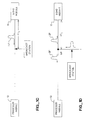
- a transceiver or other broadcasting station has just broadcast a signal in both directions on a cable 12, as illustrated in Fig. 1A; and assume that the location of this transceiver is not yet known.
- the broadcast signal will propagate in both directions on the cable 12, as illustrated in Fig. 1B.
- the propagating signal is received by an echo module 11, positioned at one end of the cable 12, and an echo pulse is broadcast by the echo module on the cable after a predetermined packet monitoring time interval of length ⁇ t d that is much less than the length of the interframe gap ⁇ t gap .
- This re-broadcast occurs in the interframe gap or quiet period that would ordinarily follow the receipt of the propagating signal. Echo pulse broadcast may occur at other times as well.
- the signal or packet originally broadcast by the transceiver is received by a processor module 13 at the other end of the cable 12, and the time t1 at which the original signal arrives at the receiver-processor module is determined by this module.
- the echo pulse broadcast by the echo module 11 then arrives at the processor module 13 at a time t2, and this time is determined by the processor module, with the same monitoring time delay ⁇ t d included in t1 and t2.
- ⁇ t dp is a time delay associated with echo pulse validation.
- a signal that is introduced onto a LAN cable 12 by a broadcast station or transceiver that is tapped into the cable will travel toward a first end of the cable and toward a second end of the cable as separate signals or packets BP, as illustrated in Fig. 1B.
- an echo module 11 is positioned at one end of the cable 12, to receive the originally broadcast packet BP and to issue an echo pulse EP, as illustrated in Fig. 1C, after a predetermined monitoring time delay ⁇ t m at the echo module 11.
- a local area network may have as many as seven layers for message processing at each station.
- the physical layer may include cables, connectors, voltage level sensors and provision for particular signal generation and propagation standards.
- the data link layer signals are exchanged by use of frames.
- a frame is a sequence of bytes, including a header that specifies source and destination of the frame and certain control and error check fields, plus the data to be transported.
- the next higher level called the network layer, transports information across the LAN in packets and is the "lowest" level that recognizes and works with the topology of the LAN.
- a packet may be a collection of frames, spaced apart by no more than a predetermined amount on the LAN cable that carries the signals.
- a local area network communication system such as Ethernet allows use of a branching, non-rooted tree network or bus topology and limits the maximum station separation to about 0.5 kilometers at the physical layer.
- one of the constraints built into the system is that, after a transceiver has either received or transmitted a message or has sensed a collision of two packets, the transceiver must remain silent and not broadcast for at least a minimum time interval of length ⁇ t gap , called the interframe gap length.
- ⁇ t gap 9.6-10.6 ⁇ sec, depending on the circumstances.
- Imposition of silence on the network for an interframe gap allows a signal that is received by a transceiver on the LAN to propagate to its destination before another such signal is launched by a transceiver that earlier received this signal. Collisions of packets propagating on the LAN are not avoided but are merely reduced in number by use of the interframe gap.
- the interframe gap time interval is used to advantage by the invention to determine the position on the network, with reasonable accuracy, of the station that last broadcast a packet on the network.
- the interframe gap time interval is used to propagate an echo pulse EP for the packet BP received on the cable 12, from the echo module 11 to the processor module 13; and formation of a simple difference in times of arrival of the two signals at the module 13 is used to determine the distance, expressed in signal propagation time, of the station that broadcast the "last" packet on the cable 12 from the echo module 11. If the broadcasting station is positioned on a branch of the LAN network that intersects the "main" cable 12, on which the echo and processor modules 11 and 13 are located, at node point NP as shown in Fig.
- Fig. 2 graphically illustrates the time line for receipt of the broadcast packet BP of the modules 11 and 13 and broadcast of an echo pulse EP by the echo module 11.
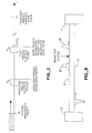
- Fig. 3 is a block diagram illustrating the major functional components of the echo module 11.
- a signal BP is received at an input terminal of the echo module 11 as shown.
- the input terminal includes a receiver-amplifier module 21 that receives a broadcast packet as a sequence of pulses and issues as an output signal a sequence of approximately square pulses having the same lengths, relative separations and relative positions as the pulses that comprise the broadcast packet received as an input signal; each pulse that is part of the packet received is reformed as an approximately square pulse, and broadcast packets with up to 20 dB of attenuation are recognized and reformed by the receiver-amplifier module 21.
- the receiver-amplifier module 21 should be capable of accurately reproducing signals with an associated frequency of up to 10 MHz or the maximum operating frequency permitted at the physical layer on the cable network, and should filter out or otherwise attenuate higher frequency cable noise. This filtering may be done by a standard arrangement of resistor and capacitor in series with a capacitor bypass to ground, where this resistor-capacitor circuit has an associated break frequency somewhere above the maximum operating frequency.
- the output signal from the receiver-amplifier module 21 is fed to a pulse modifier module 23 (optional) that receives the sequence of squared pulses that comprise the broadcast packet.
- One such pulse of temporal length ⁇ t p1 is issued in response to receipt of each pulse that is part of the packet, even though the time interval corresponding to the length of the broadcast packet may be less than 50 nsec.
- a pulse of temporal length 50 nsec is the minimum length pulse that can travel through a series of delay lines without unacceptable loss of definition. If Manchester encoding of signals is used for the LAN, each bit of such a signal comprises two consecutive components, a logical "zero" and a logical "one", each approximately 50 nsec in length. Inclusion of the pulse modifier module 23 provides a pulse of better definition.
- EOP end-of-packet
- worst case Manchester encoding of signals produces a gap or time interval of length at most 200 nsec between successive positive edges of the data.
- the circuit used for the EOP detector 25 uses 400 nsec time separation as a criterion for absence of a next pulse, because the phase shift of the receiver-amplifier module 21 can be as much as 50% on signals of varying amplitude.
- a shift in the d.c. level of the receiver-amplifier module 21 may cause that module to "hiccup" for a short period of time as it adjusts to the new d.c. bias level.
- the output signal of the receiver-amplifier module 21 is also received by a packet activity module 27 (optional) that counts the number of bits N received in the broadcast packet input signal at the echo module 11 and counts the number of packets M received. If the number N is at least equal to a predetermined positive number N1, the packet activity module 27 issues a start-of-packet ("SOP") output signal of a fifth predetermined voltage v5 and resets N to zero; and if N ⁇ N1, the module issues a SOP-absent output signal of a sixth predetermined voltage v6, indicating that the signal received at the module 11 is not a packet, and resets N to zero.
- SOP start-of-packet
- the number N1 may be chosen to be 64 or 128 or some similar number that distinguishes between the number of bits contained in a genuine packet and the number of bits received in a packet fragment that might result from collision of two such packets.
- An SOP signal of voltage v5 indicates that the echo module 11 is receiving the start of a bona fide packet.
- a packet counter within the packet activity module 27 receives and counts the SOP signals. If the number M of such SOP signals received is at least equal to a second predetermined number M2, and if N > N1, the packet activity module 27 issues a transmitter control enable signal having a seventh predetermined voltage v7; and if N ⁇ N1 or M ⁇ M2, or both, the module 27 issues an output signal having an eighth predetermined voltage v8.
- the packet counter is not required by the invention, but its inclusion allows the operator to avoid time delays associated with propagation of the echo packet BP2 and problems with signal repeaters, through control of the number M2. If M2 is chosen to be 60, for example, an echo packet will be issued by the echo module 11 at most once for every 60 broadcast packets BP1 received from the plurality of broadcasting stations on the LAN.
- the SOP counter can be effectively removed from the packet activity module 27 by setting M2 ⁇ 1.
- the output signal from the transmitter control module 31 is received by a transmitter module 33; and if this output signal has the voltage level v9, the transmitter module 33 is enabled and broadcasts an echo pulse EP on the cable that is a single, constant-amplitude pulse having a length equal to a predetermined time length ⁇ t p3 , which may be chosen to be of the order of 1 ⁇ sec.
- a monitoring delay time interval of length ⁇ t d approximately equal to 455 nsec elapses; this temporal length is known to an accuracy of within two nsec.
- the echo pulse EP will travel down the cable 12 toward the processor module 13 during the interframe gap or at any time in another embodiment. When the echo pulse EP is received by the processor module 13 at the other end of the cable 12, it is expected that no other packet or pulse will be present.
- the processor module 13 also receives the original broadcast packet BP from one of the broadcast stations that is tapped into the cable 12.
- the input signal representing the broadcast packet BP is passed through a receiver-amplifier module 41 that functions identically to the receiver-amplifier module 21 for the echo module 11.
- the output signal from the receiver-amplifier module 41 is then passed to a pulse modifier module 43 (optional) that functions identically to the pulse modifier module 23 for the echo module 11.
- a packet activity module 47 (optional) constructed similarly to the packet activity module 27 without the SOP counter for the echo module 11, receives the output signal from the receiver-amplifier module 41 and counts the number of bits N received in the input signal. If the number N is at least equal to a predetermined positive number N3, the packet activity module 47 issues a start-of-packet SOP output signal having a predetermined voltage v15; and if N ⁇ N3, the module 47 issues a SOP-absent output signal having a predetermined voltage v16.
- An echo detector 49 receives the output signal from the receiver-amplifier module 41 and determines the single-pulse length of this output signal. If the pulse length exceeds a predetermined temporal length ⁇ t p6 800 nsec, the echo detector 49 issues an echo-detected output signal having a predetermined voltage v17; and if this pulse length does not exceed the length ⁇ t p6 , the echo detector 49 issues an echo-absent output signal having a predetermined voltage v18.
- Collisions of signals are part of the environment in which a transceiver or other station operates on an LAN of this type, and the processor module 13 is provided with an optional collision detector 15 of conventional design that receives each incoming broadcast packet. If a portion of one such packet is overlapped by a portion of another such incoming packet, the collision detector 51 issues on output signal having a predetermined voltage v19, indicating that a packet collision is detected; if no packet collision is sensed by the module 51, the collision detector 51 issues an output signal having a predetermined voltage v20.
- An event timer control module 53 receives as input signals the output signals of the EOP detector 45, the packet activity module 47, the echo detector 49 and the collision detector 51 and produces a first output signal of predetermined voltage v21 if: (a) the EOP detector output signal for BP has a voltage equal to v13; (b) the packet activity and counter module output signal for BP has a voltage equal to v15; (c) the echo detector module output signal has a voltage equal to v18; and (d) (optional) the collision detector module output signal has a voltage equal to v20; this indicates that a broadcast pulse has arrived at the processor module 13. The and (d) (optionally included) are satisfied for the next packet and (c) the echo detector output signal has a voltage equal to V17; this indicates that this next packet to arrive is EP, a bona fide echo pulse.
- An event timer module 55 receives the event timer control output signal and resets to zero and activates an event timer at the time t1 of receipt of an output signal of voltage V21.
- the running of the timer in the timer module 55 is stopped at a time t2 at which the event timer module 55 receives an event timer control module output signal of voltage V22, or when the accumulated time exceeds a predetermined maximum time ⁇ t max .
- Fig. 5 illustrates the major functional groupings of electronic components and devices that comprise the echo module 11, according to one embodiment of the invention.
- the receiver-amplifier module 21 comprises a high quality amplifier unit 100 that receives the input signal from the cable 12 through a capacitor 101 and a resistor 103, arranged in series at an input terminal of the amplifier 100.
- the amplifier 100 is preferably chosen to amplify pulses having attenuation as much as 20 dB and to square each pulse so that the output signal from the amplifier 100 is a sequence of squared and amplified pulses that otherwise replicate the sequence of pulses received at the input terminal of the amplifier 100.
- An amplifier power supply 109 has a standard voltage V cc such as 5 volts and is connected to the power supply input terminal of the amplifier 100 through a resistor 105 that may have a resistance value of the order of 20 Ohms.
- the power input terminal is also grounded through a capacitor 107 that may have a value of the order of 100 nanofarads ("nf").
- Any common emitter and common base terminals of the amplifier 100 are connected to ground through a capacitor 111 that may have a value of the order of 1 nf and are also connected to the output terminal of the amplifier 100 through a resistor 113 having a resistance value of the order of 3 kilo-ohms.
- the input signal to the time delay module 117 is also fed to the input terminal of a first D-type flipflop 119.
- Each flipflop used herein is assumed to have a data input terminal D, a clock input terminal CLK, a preset input terminal PR, a clear input terminal CLR, and two output terminals for logically complementary output signals Q and Q*.
- the D-type flipflop 119 has its D input terminal held high by connection directly to the power supply 109, and its clock input terminal CLK receives the input signal delivered to the time delay module 117.
- the Q* output terminal of the flipflop 121 is connected to the clear input terminal CLR of the flipflop 119; and the Q output terminal of the flipflop 119 is connected to the clear input terminal CLR of the flipflop 121 and also serves as the source of the output signal of the pulse modifier module 23.
- two time delay modules 123 and 125 each providing up to 250 time delay, are used together to produce the desired set of 17 time delayed signals with associated time delays 0, 25, 50,. . ., 400 nsec.
- the packet activity and counter module 27 (optional) includes a monostable vibrator 129, with a first input terminal receiving the output signal from the end-of-packet signal generator 25.
- the vibrator 129 has a second input terminal and a clear input terminal CLR that are directly tied to the power supply 109.
- a fourth input terminal REX/CEX of the vibrator 129 is connected to the power supply 109 through a resistor 131 having resistance of the order of 5 kilo ohms; and a fifth input terminal CEX of the multi-vibrator 129 is connected to the power supply 109 through a series combination of the resistor 131 and a capacitor 133 that has a capacitance value of the order of 0.4 nf.
- the vibrator 129 will clear itself after a time interval of approximately 0.8 ⁇ sec.
- a monostable vibrator is an analog device having first, second and clear input terminals, fourth and fifth control input terminals denoted REX/CEX and CEX, two output terminals denoted Q and Q* that produce logically complementary output signals, and a power supply terminal denoted Vcc.
- An example of such a vibrator is the 74LS123 retriggerable monostable vibrator sold by Motorola.
- the input terminals second, clear, fourth and fifth are connected directly or indirectly to the power supply so that an internal RC circuit provides the length of the retriggering time interval.
- the multi-vibrator 129 has two output terminals, and the Q* output terminal is connected to the CLR input terminal of a first ripple counter 135 that produces a single output pulse when the count N of the counter reaches a predetermined positive integer N1.
- the clock input terminal CLK of the counter 135 receives the output signal from the EOP detector module 25, or from the amplifier-receiver module 21.
- the output signal of the counter 135 is fed to the clock input terminals CLK of each of two flipflops 137 and 139, and the Q output terminal of the vibrator 129 is connected to the clear input terminals CLR of each of these two flipflops.
- the D input terminal of the first flipflop 137 is connected directly to the power supply 109, and the D input terminal of the second flipflop 139 receives a signal from another source not yet discussed.
- the Q output terminal of the first flipflop 137 is connected to the clock input terminal CLK of a second ripple counter 141, which is assumed to produce a pulse at the output terminal thereof when the count M of this second counter reaches a second predetermined positive integer N2.
- the output terminal of the second counter 141 is connected to the D input terminal of the second flipflop 139.
- the output signal issued by the Q* output terminal of the second flipflop 139 serves as the output signal from the packet activity module 27.
- the first flipflop 137 and the second counter 141 would be deleted and the D input terminal of the second flipflop 139 would be connected to the power supply 109, either directly or through a resistor (optional) as shown for the flipflop 227 that is a part of the packet activity and counter and module 47 for the processor module 13 in Fig. 6.
- the transmitter control module 31 comprises a flipflop 141 and two monostable vibrators 143 and 151, connected as follows.
- the D input terminal and the clock input terminal of the flipflop 141 receive the output signals from the packet activity and counter module 127 and the end-of-packet detector 25, respectively, and the Q* output terminal of this flipflop issues the EOP detector output signal.
- the second input and clear input terminals of a first monostable vibrator 143 are connected to ground through a capacitor 145 that has a capacitance value of the order to 10 ⁇ f and are connected to the supply 109 through a resistor 146 (optional) that has a resistance value of the order of 5 kilo-ohms.
- a fourth input terminal of the vibrator 143 is connected to the power supply 109 through a resistor 147 that has a resistance value of the order of 70 kilo-ohms; and a fifth input terminal is connected to the power supply 109 though a series combination of the resistor 147 and a capacitor 149 having a capacitance value of the order of 1 nf.
- the Q* output terminal of the vibrator 143 is connected to the preset input terminal PR of the flipflop 141.
- the vibrator 43 will clear itself after a time interval ⁇ t v of about 30 ⁇ sec so that this part of the circuit is available to analyze another packet; in practice, any choice ⁇ t v >10 ⁇ sec would probably suffice here.
- a first input terminal of the second monostable vibrator 151 is connected to ground, and the second input and clear input terminals thereof are connected to the power supply 109.
- a fourth input terminal of the vibrator 151 is connected to the power supply through a resistor 153 having a resistance value of the order of 20 kilo-ohms; and a fifth input terminal is connected to the power supply 109 through a series combination of the resistor 153 and a capacitor 155 having a capacitance value of the order of 0.1 nf.
- the vibrator 151 will clear itself after a time interval of about 0.9 ⁇ sec.
- the Q output terminal of the vibrator 151 is connected to the first input terminal of the vibrator 143, and the Q* output terminal of the vibrator 151 is connected to the clear input terminal CLR of the flipflop 141.
- the Q output signal from the flipflop 141 is also connected to the clear input terminal CLR of the second counter 141 of the packet activity module 27 so that this Q* output signal serves as a reset signal for the packet activity module 27 and as the output signal for the transmitter control module 31 that enables the transmitter module 33.
- the transmitter module 33 receives the output signal from the transmitter control module 31, and this signal is passed through a first resistor 161 (optional) having a resistance value of the order of 500 Ohms to the base of an npn transistor 163 whose emitter is grounded.
- the base of the emitter 163 is connected to ground through a second resistor 165 (optional) that has a resistance value of the order of 500 Ohms.
- the collector of the transistor 163 is connected to the end of the cable 12 through a series combination of a resistor 167 having a resistance value of the order of 30 Ohms and a diode 167 (optional) whose anode is connected to the end of the cable 12.
- the transmitter module 33 can be implemented in many other ways as well. This completes the discussion of the embodiment of the echo module 11 shown in Fig. 5.
- Fig. 6 illustrates the major functional groupings of electronic components and devices that comprise the receiver-processor module, except the collision detector 51, which is conventional and well known in the art, the event timer control module 53, and the event timer module 55.
- the amplifier-receiver module 41 in the receiver-processor module 13 includes an amplifier 171 that amplifies signals that are attenuated up to 20 dB and squares any pulse received so that the output signal from the amplifier 171 is a sequence of squared pulses with temporal lengths and separations between consecutive pulses that are substantially those of the sequence of input pulses received in the module 41.
- the amplifier 171 receives the input signal from the end of the cable 12 through a capacitor 173 having a value of the order of 0.1 ⁇ f and a resistor 175 (optional) having a resistance value of the order of 100 Ohms.
- a common emitter terminal and a common base terminal, if any, of the amplifier are connected to ground through a capacitor 177 that may have a value of the order of 1 nf.
- a high voltage power supply 179 is connected to the power supply terminal of the amplifier 171 through a resistor 181 (optional) having a resistance value of the order of 20 Ohms, and the power supply input terminal is also connected to ground through a capacitor 183 having a capacitance value of the order of 1 nf.
- the output terminal of the amplifier 171 issues the receiver-amplifier module output signal, and this output terminal is also connected to ground through the capacitor 177.
- the receiver-amplifier module output signal is passed through a resistor 197 (optional) having a resistance value of the order of 50 Ohms to an input terminal of a multi-tap time delay module 189 that provides a 50 nsec time delay and is part of the pulse modifier module 43 (optional).
- the output signal from the module 41 is also passed to the clock input terminal CLK of a first flipflop 197, and the output signal of the time delay module 189 with associated time delay 50 nsec is passed to the clock input terminal CLK of a second flipflop 199.
- the D input terminals of the two flipflops 197 and 199 are both directly connected to the power supply 179 so that receipt of a clock pulse automatically causes issue of a pulse.
- the Q output terminal of the flipflop 199 is connected to the clear input terminal CLR of the flipflop 197, and the Q output terminal of the flipflop 197 is connected to the clear input terminal CLR of the flipflop 199 and also serves as a source of the output signal from the pulse modifier module 43.
- This first output signal of the pulse modifier module 43 is received by the end-of-packet detector 45 at the input terminal of a multi-tap time delay module that is part of the EOP detector 45.
- the time delay module for the EOP detector 45 may comprise two time delay modules 201 and 202 in a combination that provides time delayed output signals with associated time delays of 25 nsec increments from 0 nsec, up to 400 nsec.
- the time delayed output signals are collectively fed to a logical summing means 203 whose output terminal is connected to the clock input terminal of a flipflop 205.
- the D input terminal, the preset input terminal PR and the clear input terminal CLR of the flipflop 205 receive signals from sources not yet discussed, and the Q* output terminal provides the EOP detector output signal for the module 45.
- the Q output terminal of the flipflop 205 is connected to a first input terminal of a first monostable vibrator 207, which has second input and clear input terminals connected to the power supply 179.
- a fourth input terminal of the vibrator 207 is connected to the power supply 179 through a resistor 209 having resistance value of the order of 5 kilo-ohms; and a fifth input terminal 211 is connected to the power supply 179 through a series combination of the resistor 209 and a capacitor 211 having capacitance value of the order of 0.1 nf.
- the vibrator 207 will clear itself after a time interval of about 0.2 ⁇ sec.
- the Q* output terminal of the first monostable vibrator 207 is connected to the clear input terminal CLR of the flipflop 205 and to a second input terminal of a second monostable vibrator 213 whose first input terminal is grounded.
- the clear input terminal of the vibrator 213 is connected to the power supply 179; a fourth input terminal is connected to the power supply 179 through a resistor 215 having a resistor value of about 100 Ohms; and a fifth input terminal is connected to the power supply 179 through a series combination of the resistor 215 and a capacitor 217 having a capacitance value of the order of 1 nf.
- the vibrator 213 will clear itself after a time interval of about 0.1 sec.
- the Q* output terminal of the vibrator 213 is connected to the preset input terminal PR of the flipflop 205.
- the vibrator 213 will clear itself after a time interval of about 54 ⁇ sec, in order to re-enable this part of the circuit to analyze another incoming pulse.
- the packet activity and counter module 47 (optional) includes a ripple counter 219 and a monostable vibrator 221 that receive the output signal from the pulse modifier module 43, or from the receiver-amplifier module 41, at the clock input terminal and first input terminal, respectively, of the counter 219 and vibrator 221.
- the second input and clear input terminals of the vibrator 221 are connected directly to the power supply 179.
- a fourth input terminal of the vibrator 221 is connected to the power supply 179 through a resistor 223 having a resistance value of the order of 5 kilo-ohms; and a fifth input terminal of the vibrator 221 is connected to the power supply 179 through a series combination of the resistor 223 and a capacitor 215 having a capacitance value of the order of 1 nf.
- the vibrator 221 will clear itself after a time interval of about 2. 25 ⁇ sec.
- the Q* output terminal of the vibrator 221 is connected to the clear input terminal CLR of the counter 219; and the Q output terminal provides the output signal of the packet activity module 227.
- the ripple counter 219 issues a pulse at its output terminal when the count N of pulses received directly or indirectly from the receiver-amplifier module 41 exceeds a third predetermined number N3, which may be of the order of 60-130.
- the output terminal of the counter 219 is connected to the clock input terminal CLK of a flipflop 227 whose D input terminal and preset input terminal PR are connected to the power supply 179 through a resistor 229 (optional) having a resistance value of the order of 5 kilo-ohms.
- the clear input terminal CLR of the flipflop 227 is connected to the Q output terminal of the monostable vibrator 221.
- the Q* output terminal of the flipflop 227 is connected to the D input terminal of the flipflop 205.
- the Q output terminal of the vibrator 221 issues the output signal of the packet activity detector 47.
- the echo detector module 49 includes a multi-tap time delay module 189, an AND gate 195, a monostable vibrator 231 and a flipflop 233; the echo detector output signals control the reaction of the remainder of the processor module 13.
- the output signals from the time delay module 189 are passed through the AND gate 195; and the output signal thereof, with associated time delay ⁇ t dp ⁇ 250 nsec, is passed to the second input terminal of a monostable vibrator 231 whose first input terminal is grounded.
- a clear input terminal of the vibrator 231 is connected to the power supply 179; a fourth input terminal is connected to the power supply 179 through a resistor 235 having a resistance value of about 5 kilo-ohms; and a fifth input terminal is connected to the power supply 179 through a series combination of the resistor 235 and a capacitor 237 having a capacitance value of about 0.4 nf.
- the vibrator 231 will clear itself after a time interval of about 800 n sec.
- the Q* output terminal of the vibrator 231 is connected to the clock input terminal CLK of a flipflop 233 whose clear input terminal CLR receives the output signal from the packet activity module 47.
- the output signal from the AND gate 195 provides a first output signal from the echo detector module 49, indicating that the candidate pulse received from the cable 12 by way of the module 41 is at least 250 nsec in length. This output signal is also fed to the D input terminal of the flipflop 233, and the Q output terminal thereof issues a second output signal from the module 49, indicating that the candidate pulse is at least 800 nsec in length and that a "true" echo packet has arrived.
- Fig. 7 The details of the event timer control module 53 and the event timer module 55, together with certain features that are not a part of the invention, are illustrated in Fig. 7.
- the output signal from the EOP detector 45 and a processor module enable signal SUREN are received at two input terminals of an AND gate 251, and the output signal thereof is passed to the input terminal of a two-input OR gate 252 (optional) that receives at its second input terminal a signal indicating that the data being received and analyzed for some other process are valid.
- the data valid signal could, for example, be generated by analysis of data received and analyzed by a time domain reflectometer ("TDR") that may operated in parallel with the invention for purposes of determining the existence of one or more impedance discontinuities on the cable 12; the use of TDR data or other similar data is not a part of the invention disclosed and claimed here, but provision is made for such additional data inputs in order to broaden the scope of possible applications of the invention.
- TDR time domain reflectometer
- the output signal from the OR gate 252 is received by the clock input terminal CLK of a flipflop 253 whose D input terminal is connected to the power supply 179.
- the preset and clear terminals PR and CLR respectively, receive input signals from sources not yet discussed.
- each flipflop 256 and 257 is connected to the power supply 179 through a resistor 258 (optional) having a resistance value of about 1 kiloohm, and the clear input terminal CLR of each of these flipflops is connected to the Q* output of the flipflop 253 for clearing after a packet has been analyzed.
- the preset input terminal PR of each of the flipflops 256 and 257 may receive an input signal from another control source, such as a TDR, that is not a part of the invention.
- the Q* output terminal of the flipflop 256 (optional) issues an output signal indicating that some other condition such as absence of a packet collision, is met or not met; the flipflop 257 may be deleted if no other condition is required in order to initiate timing of the interval between arrival of two packets such as BP and EP at the processor module 13.
- the Q* output terminal of the flipflop 257 issues an output signal indicating that an echo packet has been received and that the processor module 13 is enabled to respond; and this output signal fed to input terminals of an AND gate 261.
- the AND gate 261 may also receive one or more Q* output control signals from one or more flipflops 256 indicating the presence of other conditions such as detection of an open cable or detection of a short on the cable in a TDR interrogation of the cable 12.
- the output signal from the AND gate 261 is passed to the D input terminal of a flipflop 263 whose clock input terminal CLK receives a periodic clock signal from an oscillator 265 that produces an output frequency of 25 MHz and a period of length 40 nsec.
- the preset and clear input terminals PR and CLR of the flipflop 263 are held at predetermined voltages V PR and V CLR so that the Q and Q* output signals of the flipflop 263 are controlled by what appears at the D input terminal thereof.
- the Q and Q* output terminals of the flipflop 263 produce the start signal and the stop signals, respectively, for the event timer module 55, corresponding to arrival of the broadcast packet BP and of the echo pulse EP.
- the output signal from the AND gate 261 is also fed to a multi-tap time delay module 275 that produces a signal with a sequence of associated time delays 5 nsec, 10 nsec, 15 nsec,..., 40 nsec, output signals from the time delay module 275 have delay times of 5-40 nsec and are fed to eight input terminals of an octal D-type flipflop 277.
- These eight input signals to the flipflop assembly 277 are inverted in order and fed to eight input terminals of a second octal D-type flipflop 279 as shown in Fig. 7.
- the clock input terminal of the flipflop assembly 277 receives the stop time output signal from the Q* output terminal of the flipflop 263 so that from one to eight consecutive flipflops of this assembly may have non-zero contents at the time the clock pulse is received, and these contents are issued as output signals.
- the clock input terminal CLK of the flipflop assembly 279 receives the start time output signal from the Q-output terminal of the flipflop 263; and from one to eight consecutive input terminals of this assembly may have non-zero contents that are issued as output signals when the start time clock pulse is received.
- the eight output signals from the flipflop assembly 277 are received by eight input terminals of a priority encoder 281 that converts the decimal number represented by the eight input signals to a binary-coded number on three output terminals thereof.
- the eight output terminals of the flipflop assembly 279 are received by eight input terminals of a second priority encoder 283 that issues a binary-coded output signal at three output terminals thereof.
- the three binary-coded output signals from each of the two priority encoders 281 and 283 are received by six input terminals of a 3X3 adder 285 having a four-bit binary output for full addition, with a fifth output terminal provided for a carry bit.
- the quantity ⁇ T1 (fine) represents the sum of the two fragments of the time interval length ⁇ T1 outside the "whole" 40 nsec time intervals defined by the clock pulse source 265.
- the start timer signal that issues from the flipflop 263 is also fed to a first counter enable input terminal ENP of each of two module 16 counters 291 and 293.
- the four input input terminals of each of the counters 291 and 293 and a second counter enable input terminal ENT of 291, are held high.
- [x] denotes the integral part of the real number x, the largest integer that is ⁇ x.
- the number ⁇ T1 (coarse) C.(40nsec) is the "coarse" component of ⁇ T1
- a collision detection module 51 as in Fig. 4 can be optionally included.
- a time domain reflectometer can be operated together with the processor module 13 to locate positions on the cable 12 where the cable impedance is substantially discontinuous, corresponding to the existence of a cable .he short, or a cable break or open, or some other malady.
- the invention may even include a source address identifier, of conventional design, to identify the source or station number of the station that has just broadcast the "lost" packet that has caused an echo pulse EP to be issued.
- the echo pulse need not be issued during the interframe gap time interval but can be issued at other times as well.
- the use of a packet collision detector as part of the processor module 13, and use of a carrier sense circuit a part of the echo module 11, is probably required as the chance of a collision with the echo packet is increased where this embodiment is used.
- the invention may also be used in an embodiment in which the broadcast pulse arrives on the LAN cable 12 and the echo pulse is broadcast on a separate, dedicated cable 14 that extends from the echo module 11 to the processor module 13, as illustrated in Fig. 8.
- Use of a separate cable would allow deletion of all of the echo detector circuitry on the processor module.
- the incoming echo pulse EP would be fed directly to the event timer module.
Abstract
T₁ = (t₂ - t₁ - Δtdp )/2,
where Δtdp is a time delay associated with validation of the echo pulse.

Description
- This invention relates to local area networks and to apparatus for determining the location of each transmitting station in a local area network.
- Although a local area network ("LAN") communications system such as Ethernet (trademark of the Xerox Corporation) allows a plurality of transceivers to tap into the cable upon which the network relies, with rather generous limits on the maximum number of transceivers and the distance of closest approach for such transceivers, it is necessary for some purposes to determine with acceptable accuracy the location of each broadcasting transceiver on the cable. Frye, in U.S. Pat. No. 3,434,049, and Oliver et al., in U.S. Pat. No. 4,766,386, disclose the use of time domain reflectometry techniques to determine whether a given cable has a substantial impedance discontinuity, indicating the presence of a cable short, an open cable or another similar problem with transmission of signals on the LAN cable. However, these techniques do not permit the determination of source identity and location, with acceptable accuracy, of a broadcasting station on the cable that is not associated with an impedance discontinuity.
- It is an object of this invention to provide apparatus that can operate within the constraints imposed by an LAN system such as Ethernet and that allows determination of location of each broadcasting transceiver on a cable in the network.
- This object is met by the invention which provides, in one embodiment, two devices, to be positioned at opposite ends of a linear cable network that contains a plurality of broadcasting transceivers. It is assumed that the LAN system has an interframe gap, similar to the 9.6-10.6 microseconds ("µsec") time interval or gap associated with an Ethernet or similar system, during which no transceiver broadcasts a signal after receipt of the immediately preceding signal.
- Assume that a transceiver or other broadcasting station has just broadcast a signal in both directions on a
cable 12, as illustrated in Fig. 1A; and assume that the location of this transceiver is not yet known. The broadcast signal will propagate in both directions on thecable 12, as illustrated in Fig. 1B. The propagating signal is received by anecho module 11, positioned at one end of thecable 12, and an echo pulse is broadcast by the echo module on the cable after a predetermined packet monitoring time interval of length Δtd that is much less than the length of the interframe gap Δtgap. This re-broadcast occurs in the interframe gap or quiet period that would ordinarily follow the receipt of the propagating signal. Echo pulse broadcast may occur at other times as well. - The signal or packet originally broadcast by the transceiver is received by a
processor module 13 at the other end of thecable 12, and the time t₁ at which the original signal arrives at the receiver-processor module is determined by this module. The echo pulse broadcast by theecho module 11 then arrives at theprocessor module 13 at a time t₂, and this time is determined by the processor module, with the same monitoring time delay Δtd included in t₁ and t₂. The length of the time interval ΔT₁ required for a signal to travel from the broadcasting transceiver to the echo module is then determined by the relation
ΔT₁ = (t₂ - t₁- Δtdp)/2.
where Δtdp is a time delay associated with echo pulse validation. -
- Figs. 1A, 1B and 1C illustrate broadcast of a packet by a station onto a cable, propagation of this packet in both directions on the cable, and broadcast of an echo packet at one end of the cable, according to the invention.
- Fig. 1D illustrates broadcast of a packet onto a cable by a station positioned on a branch of the cable.
- Fig. 2 is a graphic view of the time line for receipt and broadcast of the packets shown in Figs. 1A, 1B and 1C.
- Fig. 3 is a block diagram illustrating the overall operation of the functional blocks that comprise the echo module that is positioned at one end of an LAN cable.
- Fig. 4 is a block diagram illustrating some of the operations of the functional blocks that comprise the receiver-processor module that is positioned at a second end of an LAN cable according to the invention.
- Figs. 5, 6 and 7 are schematic circuit diagrams of the echo module, the processor module, and the event timer control and event timer modules that comprise one embodiment of the invention.
- Fig. 8 illustrates the use of two cables with the invention.
- With reference to Fig. 1A, a signal that is introduced onto a
LAN cable 12 by a broadcast station or transceiver that is tapped into the cable, will travel toward a first end of the cable and toward a second end of the cable as separate signals or packets BP, as illustrated in Fig. 1B. In one embodiment of the invention, anecho module 11 is positioned at one end of thecable 12, to receive the originally broadcast packet BP and to issue an echo pulse EP, as illustrated in Fig. 1C, after a predetermined monitoring time delay Δtm at theecho module 11. A receiver-processor module 13 positioned at a second end of thecable 12 receives the originally broadcast packet BP, notes the time t₁ of such receipt, receives the echo pulse EP and notes the time t₂ of such receipt, and determines the cable propagation time ΔT₁ from the broadcast station to theecho module 13 approximately by the relation ΔT₁ = (t₂ - t₁ - Δtdp)/2. - According to the Open Systems Interconnection ("O.S.I.") Standard proposed by Zimmerman in I.E.E.E. Trans. on Commun., vol. COM-28, 1980, pp. 425-432, and adopted by the O.S.I. Standards Committee, a local area network may have as many as seven layers for message processing at each station. At the lowest level, called the physical layer, communication between station and cable occurs in units of individual bits and/or bytes. The physical layer may include cables, connectors, voltage level sensors and provision for particular signal generation and propagation standards. In the next higher level, called the data link layer, signals are exchanged by use of frames. A frame is a sequence of bytes, including a header that specifies source and destination of the frame and certain control and error check fields, plus the data to be transported. The next higher level, called the network layer, transports information across the LAN in packets and is the "lowest" level that recognizes and works with the topology of the LAN. A packet may be a collection of frames, spaced apart by no more than a predetermined amount on the LAN cable that carries the signals.
- A local area network communication system such as Ethernet allows use of a branching, non-rooted tree network or bus topology and limits the maximum station separation to about 0.5 kilometers at the physical layer. In order to minimize or at least control packet collisions on the LAN, one of the constraints built into the system is that, after a transceiver has either received or transmitted a message or has sensed a collision of two packets, the transceiver must remain silent and not broadcast for at least a minimum time interval of length Δtgap, called the interframe gap length. For a system such as Ethernet, Δtgap = 9.6-10.6µsec, depending on the circumstances. Imposition of silence on the network for an interframe gap allows a signal that is received by a transceiver on the LAN to propagate to its destination before another such signal is launched by a transceiver that earlier received this signal. Collisions of packets propagating on the LAN are not avoided but are merely reduced in number by use of the interframe gap.
- The interframe gap time interval is used to advantage by the invention to determine the position on the network, with reasonable accuracy, of the station that last broadcast a packet on the network. The interframe gap time interval is used to propagate an echo pulse EP for the packet BP received on the
cable 12, from theecho module 11 to theprocessor module 13; and formation of a simple difference in times of arrival of the two signals at themodule 13 is used to determine the distance, expressed in signal propagation time, of the station that broadcast the "last" packet on thecable 12 from theecho module 11. If the broadcasting station is positioned on a branch of the LAN network that intersects the "main"cable 12, on which the echo andprocessor modules modules echo module 11. - Fig. 3 is a block diagram illustrating the major functional components of the
echo module 11. A signal BP is received at an input terminal of theecho module 11 as shown. The input terminal includes a receiver-amplifier module 21 that receives a broadcast packet as a sequence of pulses and issues as an output signal a sequence of approximately square pulses having the same lengths, relative separations and relative positions as the pulses that comprise the broadcast packet received as an input signal; each pulse that is part of the packet received is reformed as an approximately square pulse, and broadcast packets with up to 20 dB of attenuation are recognized and reformed by the receiver-amplifier module 21. The receiver-amplifier module 21 should be capable of accurately reproducing signals with an associated frequency of up to 10 MHz or the maximum operating frequency permitted at the physical layer on the cable network, and should filter out or otherwise attenuate higher frequency cable noise. This filtering may be done by a standard arrangement of resistor and capacitor in series with a capacitor bypass to ground, where this resistor-capacitor circuit has an associated break frequency somewhere above the maximum operating frequency. - The output signal from the receiver-
amplifier module 21 is fed to a pulse modifier module 23 (optional) that receives the sequence of squared pulses that comprise the broadcast packet. Thepulse modifier module 23 issues a single pulse or sequence of pulses having a first predetermined voltage v₁ and having a time interval of length Δtp1 = 50 nanoseconds ("nsec"), each as an output signal, if at least one square pulse is received at the input terminal, and issues a d.c. output signal of a second predetermined voltage v₂ if no square pulse is received at the input terminal of themodule 23. One such pulse of temporal length Δtp1 is issued in response to receipt of each pulse that is part of the packet, even though the time interval corresponding to the length of the broadcast packet may be less than 50 nsec. A pulse of temporal length 50 nsec is the minimum length pulse that can travel through a series of delay lines without unacceptable loss of definition. If Manchester encoding of signals is used for the LAN, each bit of such a signal comprises two consecutive components, a logical "zero" and a logical "one", each approximately 50 nsec in length. Inclusion of thepulse modifier module 23 provides a pulse of better definition. - The
pulse modifier module 23 produces an output signal that is fed to an end-of-packet ("EOP")detector 25 as an input signal. If such input signal includes a pulse of temporal length 50 nsec and of voltage v₁, theEOP detector 25 issues as an output signal a pulse of a third predetermined voltage v₃ of temporal length equal to a time interval Δtp1 + Δtp2 = 450 nsec; if thedetector 25 does not receive another input signal pulse with voltage v₁ within a time interval of length tp2 after thedetector 25 receives the immediately preceding input signal, the output signal of theEOP detector 25 makes a transition to a fourth predetermined voltage v₄. The output signal of theEOP detector 25 will thus make a transition from the voltage v₃ to the voltage v₄ only if a second pulse is not received by thedetector 25 within a time interval of length Δtp2 = 400 nsec after receipt of the preceding pulse; any time interval of length 200 nsec would probably suffice here. For a communications system such as Ethernet, worst case Manchester encoding of signals produces a gap or time interval of length at most 200 nsec between successive positive edges of the data. The circuit used for theEOP detector 25 uses 400 nsec time separation as a criterion for absence of a next pulse, because the phase shift of the receiver-amplifier module 21 can be as much as 50% on signals of varying amplitude. For example, a shift in the d.c. level of the receiver-amplifier module 21 may cause that module to "hiccup" for a short period of time as it adjusts to the new d.c. bias level. The threshold length Δtp2 associated with the end-of-packet signal generator 25 may be varied to take account of other network constraints on processing of data. If the pulse in the broadcast packet BP thus received by theecho module 11 is the "last" such pulse before an interframe gap, theEOP detector 25 will sense this and its output signal will be a pulse of length Δtp1 + Δtp2 = 450 nsec and of voltage v₃, followed by a transition to an unvarying voltage level v₄. If the pulse sensed in the broadcast packet BP is not the last pulse received before an interframe gap, the output signal of theEOP detector 25 will not make a transition to the voltage level v₄ after a time interval of length 450 nsec. - The output signal of the receiver-
amplifier module 21 is also received by a packet activity module 27 (optional) that counts the number of bits N received in the broadcast packet input signal at theecho module 11 and counts the number of packets M received. If the number N is at least equal to a predetermined positive number N₁, thepacket activity module 27 issues a start-of-packet ("SOP") output signal of a fifth predetermined voltage v₅ and resets N to zero; and if N < N₁, the module issues a SOP-absent output signal of a sixth predetermined voltage v₆, indicating that the signal received at themodule 11 is not a packet, and resets N to zero. In practice, the number N₁ may be chosen to be 64 or 128 or some similar number that distinguishes between the number of bits contained in a genuine packet and the number of bits received in a packet fragment that might result from collision of two such packets. An SOP signal of voltage v₅ indicates that theecho module 11 is receiving the start of a bona fide packet. - A packet counter within the
packet activity module 27 receives and counts the SOP signals. If the number M of such SOP signals received is at least equal to a second predetermined number M₂, and if N > N₁, thepacket activity module 27 issues a transmitter control enable signal having a seventh predetermined voltage v₇; and if N < N₁ or M < M₂, or both, themodule 27 issues an output signal having an eighth predetermined voltage v₈. - The packet counter is not required by the invention, but its inclusion allows the operator to avoid time delays associated with propagation of the echo packet BP₂ and problems with signal repeaters, through control of the number M₂. If M₂ is chosen to be 60, for example, an echo packet will be issued by the
echo module 11 at most once for every 60 broadcast packets BP₁ received from the plurality of broadcasting stations on the LAN. The SOP counter can be effectively removed from thepacket activity module 27 by setting M₂ < 1. The packet activity andcounter module 27 may be effectively deleted, for example by setting N₁ = 1 or by deleting the circuitry that performs the functions of themodule 27. - A
transmitter control module 31 receives the output signal from theEOP detector 25 and the SOP signal or the output signal from the packet activity andcounter module 27; and if the voltages associated with these two output signals have the levels v₄ and v₅ (or v₄ and v₇), respectively, thetransmitter control module 31 issues a transmitter control output signal of a ninth predetermined voltage v₉ to enable a transmitter to issue an echo pulse EP. If the output signals of one or more of theEOP detector 25 or the packet activity andcounter module 27 are not equal to v₄ or v₅, respectively, thetransmitter control module 31 issues a transmitter control output signal having a tenth predetermined voltage v₁₀ that disables or does not activate the transmitter. If themodule 31 issues a transmitter enable signal, this module also issues a reset signal that is fed back to thepacket activity module 27 to reset the SOP counter number M to M = 0. - The output signal from the
transmitter control module 31 is received by atransmitter module 33; and if this output signal has the voltage level v₉, thetransmitter module 33 is enabled and broadcasts an echo pulse EP on the cable that is a single, constant-amplitude pulse having a length equal to a predetermined time length Δtp3, which may be chosen to be of the order of 1 µsec. From the time the front end of the broadcast packet BP is received at theecho module 11 until the front end of the echo pulse EP is issued by thetransmitter module 33 onto the cable, a monitoring delay time interval of length Δtd approximately equal to 455 nsec elapses; this temporal length is known to an accuracy of within two nsec. The echo pulse EP will travel down thecable 12 toward theprocessor module 13 during the interframe gap or at any time in another embodiment. When the echo pulse EP is received by theprocessor module 13 at the other end of thecable 12, it is expected that no other packet or pulse will be present. - At the other end of the
cable 12, theprocessor module 13 also receives the original broadcast packet BP from one of the broadcast stations that is tapped into thecable 12. The input signal representing the broadcast packet BP is passed through a receiver-amplifier module 41 that functions identically to the receiver-amplifier module 21 for theecho module 11. The output signal from the receiver-amplifier module 41 is then passed to a pulse modifier module 43 (optional) that functions identically to thepulse modifier module 23 for theecho module 11. Thepulse modifier module 43 for theprocessor module 13 thus issues an output signal that is a pulse having a predetermined length Δtp4 = 50 nsec and having a predetermined voltage v₁₁, if at least one pulse is received by themodule 43; and themodule 43 issues a d.c. output signal having a predetermined voltage v₁₂ if no pulse is received at themodule 43. An end-of-packet detector 45, constructed similarly to theEOP detector 25 for theecho module 11, receives the output signal from thepulse modifier module 43; and if the pulse received by theprocessor module 13 is the last pulse before an interframe gap, theEOP detector 45 will produce a single pulse of predetermined voltage v₁₃ having length Δtp4 +Δtp5, = 450 nsec followed by transition to a d.c. signal having a predetermined voltage v₁₄. - A packet activity module 47 (optional) constructed similarly to the
packet activity module 27 without the SOP counter for theecho module 11, receives the output signal from the receiver-amplifier module 41 and counts the number of bits N received in the input signal. If the number N is at least equal to a predetermined positive number N₃, thepacket activity module 47 issues a start-of-packet SOP output signal having a predetermined voltage v₁₅; and if N < N₃, themodule 47 issues a SOP-absent output signal having a predetermined voltage v₁₆. - An
echo detector 49 receives the output signal from the receiver-amplifier module 41 and determines the single-pulse length of this output signal. If the pulse length exceeds a predetermined temporal length Δtp6 800 nsec, theecho detector 49 issues an echo-detected output signal having a predetermined voltage v₁₇; and if this pulse length does not exceed the length Δtp6, theecho detector 49 issues an echo-absent output signal having a predetermined voltage v₁₈. The temporal length tp6 may be chosen to be about 800 nsec if the temporal length Δtp3 = 1µsec; in any event, Δtp6 is chosen to be less than but approximately equal to Δtp3. - Collisions of signals are part of the environment in which a transceiver or other station operates on an LAN of this type, and the
processor module 13 is provided with an optional collision detector 15 of conventional design that receives each incoming broadcast packet. If a portion of one such packet is overlapped by a portion of another such incoming packet, thecollision detector 51 issues on output signal having a predetermined voltage v₁₉, indicating that a packet collision is detected; if no packet collision is sensed by themodule 51, thecollision detector 51 issues an output signal having a predetermined voltage v₂₀. - An event
timer control module 53 receives as input signals the output signals of theEOP detector 45, thepacket activity module 47, theecho detector 49 and thecollision detector 51 and produces a first output signal of predetermined voltage v₂₁ if: (a) the EOP detector output signal for BP has a voltage equal to v₁₃; (b) the packet activity and counter module output signal for BP has a voltage equal to v₁₅; (c) the echo detector module output signal has a voltage equal to v₁₈; and (d) (optional) the collision detector module output signal has a voltage equal to v₂₀; this indicates that a broadcast pulse has arrived at theprocessor module 13. The
and (d) (optionally included) are satisfied for the next packet and (c) the echo detector output signal has a voltage equal to V₁₇; this indicates that this next packet to arrive is EP, a bona fide echo pulse. - An
event timer module 55 receives the event timer control output signal and resets to zero and activates an event timer at the time t₁ of receipt of an output signal of voltage V₂₁. The running of the timer in thetimer module 55 is stopped at a time t₂ at which theevent timer module 55 receives an event timer control module output signal of voltage V₂₂, or when the accumulated time exceeds a predetermined maximum time Δtmax. The accumulated time t on the timer between the point at which the timer is reset and started, representing receipt of BP, and the time at which the timer is stopped, representing receipt of EP, is the difference Δt = t₂ - t₁ of times of arrival of the front ends of the broadcast packets BP and EP at theprocessor module 13 with the time delay Δtd incorporated in each of the times t₁ and t₂. The distance, measured in signal propagation time on thecable 12, from the station that broadcasts the packet BP and theecho module 11 is then determined by the relat-ion ΔT₁ = (Δt- Δtdp) /2. - Fig. 5 illustrates the major functional groupings of electronic components and devices that comprise the
echo module 11, according to one embodiment of the invention. The receiver-amplifier module 21 comprises a highquality amplifier unit 100 that receives the input signal from thecable 12 through acapacitor 101 and aresistor 103, arranged in series at an input terminal of theamplifier 100. Theamplifier 100 is preferably chosen to amplify pulses having attenuation as much as 20 dB and to square each pulse so that the output signal from theamplifier 100 is a sequence of squared and amplified pulses that otherwise replicate the sequence of pulses received at the input terminal of theamplifier 100. Anamplifier power supply 109 has a standard voltage Vcc such as 5 volts and is connected to the power supply input terminal of theamplifier 100 through aresistor 105 that may have a resistance value of the order of 20 Ohms. The power input terminal is also grounded through acapacitor 107 that may have a value of the order of 100 nanofarads ("nf"). Any common emitter and common base terminals of theamplifier 100 are connected to ground through a capacitor 111 that may have a value of the order of 1 nf and are also connected to the output terminal of theamplifier 100 through aresistor 113 having a resistance value of the order of 3 kilo-ohms. - The pulse modifier module 23 (optional) receives the output signal of the receiver-
amplifier module 21 through aresistor 115 having a resistance value of the order of 50 Ohms, and this signal is passed to the input terminal of atime delay module 117 that produces an output signal that is a replica of the input signal but delayed by a time Δtp1 = 50 nsec. - The input signal to the
time delay module 117 is also fed to the input terminal of a first D-type flipflop 119. Each flipflop used herein is assumed to have a data input terminal D, a clock input terminal CLK, a preset input terminal PR, a clear input terminal CLR, and two output terminals for logically complementary output signals Q and Q*. The D-type flipflop 119 has its D input terminal held high by connection directly to thepower supply 109, and its clock input terminal CLK receives the input signal delivered to thetime delay module 117. Asecond flipflop 121 also has its D input held high by direct connection to thepower supply 109, and its clock input terminal CLK receives the output signal, with the associated time delay of Δtp1 =50 nsec, from thetime delay module 117. The Q* output terminal of theflipflop 121 is connected to the clear input terminal CLR of theflipflop 119; and the Q output terminal of theflipflop 119 is connected to the clear input terminal CLR of theflipflop 121 and also serves as the source of the output signal of thepulse modifier module 23. The two clock input terminals CLK of theflipflops flipflop 121 is used to clear theflipflop 119. The result is a pulse of temporal length Δtp1 = 50 nsec at the Q output terminal of theflipflop 119, if the input signal to thepulse modifier module 23 has a temporal length of any amount that can be sensed by theflipflops - The
EOP detector module 25 includes one or more multi-tap time delay modules that produce a plurality of output signals that are time delayed relative to one another by approximately 25 nsec or an integral multiple thereof. A sequence of such time delayed output signals is produced with a maximum time delay of Δtp2 = 400 nsec as indicated; again, any Δtd2> 200 nsec would probably suffice here. In the embodiment shown in Fig. 5, twotime delay modules time delays 0, 25, 50,. . ., 400 nsec. The output signals from the time delay module or modules are fed to a logical summingmeans 127, whose output signal is thus a single pulse of temporal length Δtp1 + Δtp2 = 450 nsec. At the end of this pulse, the output signal changes to a different voltage unless another input signal to theEOP detector module 25 has been received within a time interval of length Δtp2 = 400 nsec after receipt of the immediately preceding pulse. - Under a worst case Manchester encoding circumstance on Ethernet at 10 MHz, successive positive edges of the incoming data would be separated by at most 200 nsec; and a pulse stand-off time of Δtp2 = 400 nsec is used here to compensate for possible degradation of signals. If no incoming pulse follows another incoming pulse within 200 nsec in time, it is assumed that the present pulse is the last pulse of a packet received by the
echo module 11; and the result of this is that the output signal from theEOP detector module 25 is a pulse of length Δtp1 + Δtp2 = 450 nsec, followed by a transition to a different voltage level. - The packet activity and counter module 27 (optional) includes a
monostable vibrator 129, with a first input terminal receiving the output signal from the end-of-packet signal generator 25. Thevibrator 129 has a second input terminal and a clear input terminal CLR that are directly tied to thepower supply 109. A fourth input terminal REX/CEX of thevibrator 129 is connected to thepower supply 109 through aresistor 131 having resistance of the order of 5 kilo ohms; and a fifth input terminal CEX of the multi-vibrator 129 is connected to thepower supply 109 through a series combination of theresistor 131 and acapacitor 133 that has a capacitance value of the order of 0.4 nf. Thevibrator 129 will clear itself after a time interval of approximately 0.8 µsec. - As used herein, a monostable vibrator is an analog device having first, second and clear input terminals, fourth and fifth control input terminals denoted REX/CEX and CEX, two output terminals denoted Q and Q* that produce logically complementary output signals, and a power supply terminal denoted Vcc. An example of such a vibrator is the 74LS123 retriggerable monostable vibrator sold by Motorola. In one mode of use, the input terminals second, clear, fourth and fifth are connected directly or indirectly to the power supply so that an internal RC circuit provides the length of the retriggering time interval. However, a resistor of resistance value RE may be connected between the REX/CEX terminal and the power supply, and a capacitor of capacitance value CE together with this resistor may be connected in series between the CEX terminal and the power supply; and the time constant τ associated with the retriggering time interval then becomes an adjustable parameter, viz. τ = K(RE)(CE), where K is a numerical constant, equal to approximately 0.45 for the Motorola 74LS123 vibrator.
- The multi-vibrator 129 has two output terminals, and the Q* output terminal is connected to the CLR input terminal of a
first ripple counter 135 that produces a single output pulse when the count N of the counter reaches a predetermined positive integer N₁. The clock input terminal CLK of thecounter 135 receives the output signal from theEOP detector module 25, or from the amplifier-receiver module 21. The output signal of thecounter 135 is fed to the clock input terminals CLK of each of twoflipflops vibrator 129 is connected to the clear input terminals CLR of each of these two flipflops. The D input terminal of thefirst flipflop 137 is connected directly to thepower supply 109, and the D input terminal of thesecond flipflop 139 receives a signal from another source not yet discussed. The Q output terminal of thefirst flipflop 137 is connected to the clock input terminal CLK of asecond ripple counter 141, which is assumed to produce a pulse at the output terminal thereof when the count M of this second counter reaches a second predetermined positive integer N₂. The output terminal of thesecond counter 141 is connected to the D input terminal of thesecond flipflop 139. The output signal issued by the Q* output terminal of thesecond flipflop 139 serves as the output signal from thepacket activity module 27. - In an embodiment of the invention in which the number M of packets received is not counted, the
first flipflop 137 and thesecond counter 141 would be deleted and the D input terminal of thesecond flipflop 139 would be connected to thepower supply 109, either directly or through a resistor (optional) as shown for theflipflop 227 that is a part of the packet activity and counter andmodule 47 for theprocessor module 13 in Fig. 6. - The
transmitter control module 31 comprises aflipflop 141 and twomonostable vibrators flipflop 141 receive the output signals from the packet activity andcounter module 127 and the end-of-packet detector 25, respectively, and the Q* output terminal of this flipflop issues the EOP detector output signal. - The second input and clear input terminals of a first
monostable vibrator 143 are connected to ground through acapacitor 145 that has a capacitance value of the order to 10 µf and are connected to thesupply 109 through a resistor 146 (optional) that has a resistance value of the order of 5 kilo-ohms. A fourth input terminal of thevibrator 143 is connected to thepower supply 109 through aresistor 147 that has a resistance value of the order of 70 kilo-ohms; and a fifth input terminal is connected to thepower supply 109 though a series combination of theresistor 147 and acapacitor 149 having a capacitance value of the order of 1 nf. The Q* output terminal of thevibrator 143 is connected to the preset input terminal PR of theflipflop 141. Thevibrator 43 will clear itself after a time interval Δtv of about 30 µsec so that this part of the circuit is available to analyze another packet; in practice, any choice Δtv >10 µsec would probably suffice here. - A first input terminal of the second
monostable vibrator 151 is connected to ground, and the second input and clear input terminals thereof are connected to thepower supply 109. A fourth input terminal of thevibrator 151 is connected to the power supply through aresistor 153 having a resistance value of the order of 20 kilo-ohms; and a fifth input terminal is connected to thepower supply 109 through a series combination of theresistor 153 and acapacitor 155 having a capacitance value of the order of 0.1 nf. Thevibrator 151 will clear itself after a time interval of about 0.9 µsec. The Q output terminal of thevibrator 151 is connected to the first input terminal of thevibrator 143, and the Q* output terminal of thevibrator 151 is connected to the clear input terminal CLR of theflipflop 141. The Q output signal from theflipflop 141 is also connected to the clear input terminal CLR of thesecond counter 141 of thepacket activity module 27 so that this Q* output signal serves as a reset signal for thepacket activity module 27 and as the output signal for thetransmitter control module 31 that enables thetransmitter module 33. - The
transmitter module 33 receives the output signal from thetransmitter control module 31, and this signal is passed through a first resistor 161 (optional) having a resistance value of the order of 500 Ohms to the base of annpn transistor 163 whose emitter is grounded. The base of theemitter 163 is connected to ground through a second resistor 165 (optional) that has a resistance value of the order of 500 Ohms. The collector of thetransistor 163 is connected to the end of thecable 12 through a series combination of aresistor 167 having a resistance value of the order of 30 Ohms and a diode 167 (optional) whose anode is connected to the end of thecable 12. Thetransmitter module 33 can be implemented in many other ways as well. This completes the discussion of the embodiment of theecho module 11 shown in Fig. 5. - Fig. 6 illustrates the major functional groupings of electronic components and devices that comprise the receiver-processor module, except the
collision detector 51, which is conventional and well known in the art, the eventtimer control module 53, and theevent timer module 55. - The amplifier-
receiver module 41 in the receiver-processor module 13 includes an amplifier 171 that amplifies signals that are attenuated up to 20 dB and squares any pulse received so that the output signal from the amplifier 171 is a sequence of squared pulses with temporal lengths and separations between consecutive pulses that are substantially those of the sequence of input pulses received in themodule 41. The amplifier 171 receives the input signal from the end of thecable 12 through acapacitor 173 having a value of the order of 0.1 µf and a resistor 175 (optional) having a resistance value of the order of 100 Ohms. A common emitter terminal and a common base terminal, if any, of the amplifier are connected to ground through acapacitor 177 that may have a value of the order of 1 nf. A highvoltage power supply 179 is connected to the power supply terminal of the amplifier 171 through a resistor 181 (optional) having a resistance value of the order of 20 Ohms, and the power supply input terminal is also connected to ground through a capacitor 183 having a capacitance value of the order of 1 nf. The output terminal of the amplifier 171 issues the receiver-amplifier module output signal, and this output terminal is also connected to ground through thecapacitor 177. - The receiver-amplifier module output signal is passed through a resistor 197 (optional) having a resistance value of the order of 50 Ohms to an input terminal of a multi-tap
time delay module 189 that provides a 50 nsec time delay and is part of the pulse modifier module 43 (optional). The output signal from themodule 41 is also passed to the clock input terminal CLK of afirst flipflop 197, and the output signal of thetime delay module 189 with associated time delay 50 nsec is passed to the clock input terminal CLK of asecond flipflop 199. The D input terminals of the twoflipflops power supply 179 so that receipt of a clock pulse automatically causes issue of a pulse. The Q output terminal of theflipflop 199 is connected to the clear input terminal CLR of theflipflop 197, and the Q output terminal of theflipflop 197 is connected to the clear input terminal CLR of theflipflop 199 and also serves as a source of the output signal from thepulse modifier module 43. The output signal from themodule 43 is again a pulse of temporal length Δtp4 = 50 nsec. - This first output signal of the
pulse modifier module 43 is received by the end-of-packet detector 45 at the input terminal of a multi-tap time delay module that is part of theEOP detector 45. As shown in the embodiment of Fig. 6, the time delay module for theEOP detector 45 may comprise twotime delay modules means 203 whose output terminal is connected to the clock input terminal of aflipflop 205. - The D input terminal, the preset input terminal PR and the clear input terminal CLR of the
flipflop 205 receive signals from sources not yet discussed, and the Q* output terminal provides the EOP detector output signal for themodule 45. The Q output terminal of theflipflop 205 is connected to a first input terminal of a firstmonostable vibrator 207, which has second input and clear input terminals connected to thepower supply 179. A fourth input terminal of thevibrator 207 is connected to thepower supply 179 through aresistor 209 having resistance value of the order of 5 kilo-ohms; and a fifth input terminal 211 is connected to thepower supply 179 through a series combination of theresistor 209 and a capacitor 211 having capacitance value of the order of 0.1 nf. Thevibrator 207 will clear itself after a time interval of about 0.2 µsec. The Q* output terminal of the firstmonostable vibrator 207 is connected to the clear input terminal CLR of theflipflop 205 and to a second input terminal of a secondmonostable vibrator 213 whose first input terminal is grounded. The clear input terminal of thevibrator 213 is connected to thepower supply 179; a fourth input terminal is connected to thepower supply 179 through aresistor 215 having a resistor value of about 100 Ohms; and a fifth input terminal is connected to thepower supply 179 through a series combination of theresistor 215 and acapacitor 217 having a capacitance value of the order of 1 nf. Thevibrator 213 will clear itself after a time interval of about 0.1 sec. The Q* output terminal of thevibrator 213 is connected to the preset input terminal PR of theflipflop 205. Thevibrator 213 will clear itself after a time interval of about 54 µsec, in order to re-enable this part of the circuit to analyze another incoming pulse. - The packet activity and counter module 47 (optional) includes a ripple counter 219 and a
monostable vibrator 221 that receive the output signal from thepulse modifier module 43, or from the receiver-amplifier module 41, at the clock input terminal and first input terminal, respectively, of the counter 219 andvibrator 221. The second input and clear input terminals of thevibrator 221 are connected directly to thepower supply 179. A fourth input terminal of thevibrator 221 is connected to thepower supply 179 through aresistor 223 having a resistance value of the order of 5 kilo-ohms; and a fifth input terminal of thevibrator 221 is connected to thepower supply 179 through a series combination of theresistor 223 and acapacitor 215 having a capacitance value of the order of 1 nf. Thevibrator 221 will clear itself after a time interval of about 2. 25 µsec. The Q* output terminal of thevibrator 221 is connected to the clear input terminal CLR of the counter 219; and the Q output terminal provides the output signal of thepacket activity module 227. The ripple counter 219 issues a pulse at its output terminal when the count N of pulses received directly or indirectly from the receiver-amplifier module 41 exceeds a third predetermined number N₃, which may be of the order of 60-130. - The output terminal of the counter 219 is connected to the clock input terminal CLK of a
flipflop 227 whose D input terminal and preset input terminal PR are connected to thepower supply 179 through a resistor 229 (optional) having a resistance value of the order of 5 kilo-ohms. The clear input terminal CLR of theflipflop 227 is connected to the Q output terminal of themonostable vibrator 221. The Q* output terminal of theflipflop 227 is connected to the D input terminal of theflipflop 205. The Q output terminal of thevibrator 221 issues the output signal of thepacket activity detector 47. - The
echo detector module 49 includes a multi-taptime delay module 189, an ANDgate 195, amonostable vibrator 231 and aflipflop 233; the echo detector output signals control the reaction of the remainder of theprocessor module 13. The output signals from thetime delay module 189 are passed through the ANDgate 195; and the output signal thereof, with associated time delay Δtdp≈250 nsec, is passed to the second input terminal of amonostable vibrator 231 whose first input terminal is grounded. A clear input terminal of thevibrator 231 is connected to thepower supply 179; a fourth input terminal is connected to thepower supply 179 through aresistor 235 having a resistance value of about 5 kilo-ohms; and a fifth input terminal is connected to thepower supply 179 through a series combination of theresistor 235 and acapacitor 237 having a capacitance value of about 0.4 nf. Thevibrator 231 will clear itself after a time interval of about 800 n sec. The Q* output terminal of thevibrator 231 is connected to the clock input terminal CLK of aflipflop 233 whose clear input terminal CLR receives the output signal from thepacket activity module 47. The output signal from the ANDgate 195 provides a first output signal from theecho detector module 49, indicating that the candidate pulse received from thecable 12 by way of themodule 41 is at least 250 nsec in length. This output signal is also fed to the D input terminal of theflipflop 233, and the Q output terminal thereof issues a second output signal from themodule 49, indicating that the candidate pulse is at least 800 nsec in length and that a "true" echo packet has arrived. - The details of the event
timer control module 53 and theevent timer module 55, together with certain features that are not a part of the invention, are illustrated in Fig. 7. The output signal from theEOP detector 45 and a processor module enable signal SUREN are received at two input terminals of an ANDgate 251, and the output signal thereof is passed to the input terminal of a two-input OR gate 252 (optional) that receives at its second input terminal a signal indicating that the data being received and analyzed for some other process are valid. The data valid signal could, for example, be generated by analysis of data received and analyzed by a time domain reflectometer ("TDR") that may operated in parallel with the invention for purposes of determining the existence of one or more impedance discontinuities on thecable 12; the use of TDR data or other similar data is not a part of the invention disclosed and claimed here, but provision is made for such additional data inputs in order to broaden the scope of possible applications of the invention. The output signal from theOR gate 252 is received by the clock input terminal CLK of aflipflop 253 whose D input terminal is connected to thepower supply 179. The preset and clear terminals PR and CLR, respectively, receive input signals from sources not yet discussed. The first echo detector output signal, received from the ANDgate 195 illustrated in Fig. 6, and the processor enable signal SUREN are received at two inputs of an ANDgate 255 whose output signal is passed to the clock input terminal CLK of each of two ormore flipflops flipflop power supply 179 through a resistor 258 (optional) having a resistance value of about 1 kiloohm, and the clear input terminal CLR of each of these flipflops is connected to the Q* output of theflipflop 253 for clearing after a packet has been analyzed. The preset input terminal PR of each of theflipflops flipflop 257 may be deleted if no other condition is required in order to initiate timing of the interval between arrival of two packets such as BP and EP at theprocessor module 13. - The Q* output terminal of the
flipflop 257 issues an output signal indicating that an echo packet has been received and that theprocessor module 13 is enabled to respond; and this output signal fed to input terminals of an ANDgate 261. The ANDgate 261 may also receive one or more Q* output control signals from one ormore flipflops 256 indicating the presence of other conditions such as detection of an open cable or detection of a short on the cable in a TDR interrogation of thecable 12. - The output signal from the AND
gate 261 is passed to the D input terminal of aflipflop 263 whose clock input terminal CLK receives a periodic clock signal from anoscillator 265 that produces an output frequency of 25 MHz and a period of length 40 nsec. The preset and clear input terminals PR and CLR of theflipflop 263 are held at predetermined voltages VPR and VCLR so that the Q and Q* output signals of theflipflop 263 are controlled by what appears at the D input terminal thereof. The Q and Q* output terminals of theflipflop 263 produce the start signal and the stop signals, respectively, for theevent timer module 55, corresponding to arrival of the broadcast packet BP and of the echo pulse EP. - The output signal from the AND
gate 261 is also fed to a multi-taptime delay module 275 that produces a signal with a sequence of associated time delays 5 nsec, 10 nsec, 15 nsec,..., 40 nsec, output signals from thetime delay module 275 have delay times of 5-40 nsec and are fed to eight input terminals of an octal D-type flipflop 277. These eight input signals to theflipflop assembly 277 are inverted in order and fed to eight input terminals of a second octal D-type flipflop 279 as shown in Fig. 7. The clock input terminal of theflipflop assembly 277 receives the stop time output signal from the Q* output terminal of theflipflop 263 so that from one to eight consecutive flipflops of this assembly may have non-zero contents at the time the clock pulse is received, and these contents are issued as output signals. In a similar manner, the clock input terminal CLK of theflipflop assembly 279 receives the start time output signal from the Q-output terminal of theflipflop 263; and from one to eight consecutive input terminals of this assembly may have non-zero contents that are issued as output signals when the start time clock pulse is received. The eight output signals from theflipflop assembly 277 are received by eight input terminals of a priority encoder 281 that converts the decimal number represented by the eight input signals to a binary-coded number on three output terminals thereof. In a similar manner, the eight output terminals of theflipflop assembly 279 are received by eight input terminals of a second priority encoder 283 that issues a binary-coded output signal at three output terminals thereof. The three binary-coded output signals from each of the two priority encoders 281 and 283 are received by six input terminals of a 3X3 adder 285 having a four-bit binary output for full addition, with a fifth output terminal provided for a carry bit. The output signals from the adder 285 represent a binary-coded value corresponding to time increments of 0, 5, 10, 15,..., 75 nsec, which correspond to the 2⁴ = 16 possible output values of the adder 285. - The four output terminals I1, I2, I3 and I4 of the adder 285 contain all available information on the "fine" component of the time interval length T₁; that is, with an integer F defined by F = 8 . I4 + 4 . I3 + 2 "zero" or a logical "one", the "fine" component of T₁ is defined by ΔT₁ (fine) = F . (5 nsec) and is thus graduated in increments of 5 nsec. The quantity ΔT₁ (fine) represents the sum of the two fragments of the time interval length ΔT₁ outside the "whole" 40 nsec time intervals defined by the
clock pulse source 265. - The start timer signal that issues from the
flipflop 263 is also fed to a first counter enable input terminal ENP of each of two module 16counters counters - The carry out output terminal Co of the
counter 291, which issues a pulse each time thecounter 291 cycles from 15 to 0 modulo 16, is connected to a second counter enable terminal ENT of the second modulo 16counter 293. The twocounters event timer module 55 has been started by arrival of the broadcast packet BP and has been stopped by arrival of the echo pulse EP, the combined output signals from the twocounters
ΔT₁ = ΔT₁ (coarse) + ΔT₁ (fine) -Δtdp = C.(40 nsec) + F.(5 nsec) - Δtdp,
where Δtdp is the time delay introduced by the echo detector. - Various features can be added to the invention as disclosed here. As noted above, a
collision detection module 51 as in Fig. 4 can be optionally included. A time domain reflectometer can be operated together with theprocessor module 13 to locate positions on thecable 12 where the cable impedance is substantially discontinuous, corresponding to the existence of a cable .he short, or a cable break or open, or some other malady. The invention may even include a source address identifier, of conventional design, to identify the source or station number of the station that has just broadcast the "lost" packet that has caused an echo pulse EP to be issued. - The echo pulse need not be issued during the interframe gap time interval but can be issued at other times as well. However, in such an embodiment the use of a packet collision detector as part of the
processor module 13, and use of a carrier sense circuit a part of theecho module 11, is probably required as the chance of a collision with the echo packet is increased where this embodiment is used. - The invention may also be used in an embodiment in which the broadcast pulse arrives on the
LAN cable 12 and the echo pulse is broadcast on a separate,dedicated cable 14 that extends from theecho module 11 to theprocessor module 13, as illustrated in Fig. 8. Use of a separate cable would allow deletion of all of the echo detector circuitry on the processor module. Within theprocessor module 13, the incoming echo pulse EP would be fed directly to the event timer module.
Claims (23)
an echo module, positioned at a first end of a cable, to receive a broadcast packet, to determine whether a pulse in the packet is the last pulse received before an interframe time interval and whether at least a predetermined number of broadcast packets have been received, and if both these conditions are satisfied to broadcast an echo pulse on the cable network after a predetermined time delay Δtd, where Δtd « Δtgap; and
a processor module, positioned at a second end of the cable, to receive a broadcast packet, to determine the time t₁, including a time delay Δtdp, at which the broadcast packet arrives at the processor module, to receive an echo pulse signal, to determine the time t₂ at which the echo pulse arrives at the processor module, and to determine the time interval ΔT₁ required for a signal to travel from the broadcasting station to the echo module by the relation ΔT₁ = (t₂ - t₁-Δtdp)/2.
a receiver-amplifier module to receive a broadcast packet as a sequence of one or more pulses, to amplify and reform each pulse as a squared pulse, and to issue this sequence of squared pulses as an output signal;
an end-of-packet detector to receive the receiver-amplifier modifier module output signal as an input signal and to issue as an output signal a pulse of length Δtp2 of a predetermined voltage v₃, where Δtp2 is a predetermined time interval length, and, if this detector does not receive another non-zero input signal within a time interval of length Δtp2 after the detector receives the immediately preceding input signal, the output signal of this detector makes a transition to a predetermined voltage v₄;
a packet activity and counter module to receive the output signal from the receiver-amplifier modifier module, to count the number N of bits received in this signal, if the number of bits received is at least equal to a first predetermined number N₁ to issue a start-of-packet output signal of a predetermined voltage v₅, and if N < N₁ to issue a start-of-packet output signal of a predetermined voltage v₆;
a transmitter control module to receive the output signals from the end-of-packet detector module and from the packet activity and counter module, when these signals have voltages equal to v₄ and v₅, respectively, to issue an output signal of a predetermined voltage v₉ as an output signal, and when at least one of the output signals from the end-of-packet detector module or from the packet activity and counter module does not have a voltage equal to v₄ or v₅, respectively, to issue an output signal of a predetermined voltage v₁₀; and
a transmitter module to receive the transmitter control module output signal and, when this signal has a voltage equal to v₉, to issue said echo pulse on said cable.
a pulse modifier module to receive said receiver-amplifier module output signal, to issue an output signal to said end-of-packet detector that is a single pulse of a predetermined voltage v₁ and of length equal to a predetermined time interval Δtp1 if a non-zero input signal is received, and to issue an output signal to said end-of-packet detector that is a substantially constant, predetermined voltage v₂ if no non-zero input signal is received.
first and second signal propagation lines to receive and propagate said receiver-amplifier module output signal, where the second signal line introduces a time delay of said predetermined amount Δtp1 relative to the first signal line; and
first and second flipflops, each having a data input terminal and a clock input terminal, whose data input terminals are held at high voltages, with the first and second signal lines being connected to the clock input terminals of the first and second flipflops, respectively, where the Q* output terminal of the second flipflop is connected to the clear input terminal of the first flipflop, and the Q output terminal of the first flipflop issues said output signal from said pulse modifier module and is connected to the clear input terminal of the second flipflop.
a delay line module having an input terminal to receive said pulse modifier module output signal and having a plurality of K consecutive time delay output terminals where K is a positive integer, and each delay line module reproduces the input signal with a predetermined time delay Δtc relative to the output signal from the immediately preceding time delay output terminal, where Δtc < Δtp1 and K Δtc ≧ Δtp2; and
logical summing means for receiving the output signals from delay line module output terminals, for forming the logical sum of these signals and for issuing this logical sum of said output signal of said end-of-packet detector module.
a monostable vibrator having a first input terminal to receive said pulse modifier module output signal, having a second input terminal and a clear input terminal connected to a high voltage source, having a Q output terminal to issue an output signal pulse of predetermined temporal length Δtv each time a pulse is received at the input terminal, and having a Q* output terminal;
a pulse counter having an input terminal connected to the Q* output terminal of the monostable vibrator and having a clock input terminal connected to receive said pulse modifier module output signal, where the pulse counter has an output terminal that issues a counter output signal that is a pulse and that resets to zero each time the counter reaches a count N ≧ N₁, where N₁ is a predetermined positive number; and
a flipflop, having data input and preset input terminals that are connected to a high voltage source, having a clock input terminal that receives the counter output signal, having a flipflop clear terminal that is connected to the Q output terminal of the monostable vibrator, and having a Q* output terminal that issues said start-of-packet output signal.
a second flipflop, having data input and preset input terminals that are connected to a high voltage, having a clock input terminal that is connected to said first counter output terminal, having a clear input terminal that is connected to said Q output terminal of said monostable vibrator, and having a Q* output terminal; and
a second pulse counter having a clock input terminal connected to the Q output terminal of the second flipflop and having a clear input terminal that receives a clear input signal from an external source, where the second counter has an output terminal that is connected to said data input terminal of said first flipflop and that issues a second counter output signal that is a pulse and that resets to zero each time the second counter reaches a count L, where L is a predetermined positive integer.
a flipflop having a data input terminal to receive said packet activity and counter module output signal, having a clock input terminal to receive said end-of-packet detector output signal, and having a preset input terminal, a clear input terminal and a Q* output terminal, to issue a transmitter enable signal at the Q* output terminal;
a first monostable vibrator having a first input terminal that is grounded, having a second input terminal and a clear input terminal connected to a high voltage source, having a Q output terminal to issue an output signal pulse of predetermined temporal length Δtv1 each time a pulse is received at the first input terminal, and having a Q* output terminal that is connected to the clear input terminal of the flipflop;
a second monostable vibrator having a first input terminal connected to the Q output terminal of the first monostable vibrator, having a second input terminal and a clear input terminal connected to a high voltage source, and having a Q* output terminal connected to the preset input terminal of the flipflop to produce an output signal pulse of predetermined temporal length Δtv2 each time a pulse is received at the first input terminal.
a transistor with its emitter grounded and its base connected to ground through a resistor and positioned to receive said transmitter control module output signal;
a diode with its cathode connected to the transistor collector and its anode connected to said first end of said cable.
a receiver-amplifier module to receive a broadcast packet as a sequence of one or more pulses, to amplify and reform each pulse as a squared pulse, and to issue this sequence of squared pulses as an output signal;
an end-of-packet detector to receive the receiver-amplifier module output signal as an input signal, to issue as an output signal a pulse of a predetermined voltage v₁₃ and of length equal to a predetermined time interval Δtp5, where Δtp5 is a second predetermined time interval length, and, if this detector does not receive another non-zero input signal within a time interval of length Δtp5 after the detector receives the immediately preceding input signal, the output signal of this detector makes a transition to a predetermined voltage v₁₄;
a packet activity and counter module to receive the output signal from the receiver-amplifier module, to count the number N of bits received in this signal, if N is at least equal to a predetermined positive number N₃ to issue a start-of-packet output signal of a predetermined voltage v₁₅, and if N < N₃ to issue start-of-packet output signal of a predetermined voltage v₁₆;
an echo detector to receive the receiver-amplifier module output signal and determine the pulse length of this signal, where, if the pulse length exceeds a predetermined length Δtp6, the echo detector issues an output signal of a predetermined voltage v₁₇, and if the pulse length does not exceed the length Δtp6 the echo detector issues an output signal of predetermined voltage v₁₈, where the echo detector has an associated time delay of Δtdp;
an event timer control module to receive as input signals the output signals of the end-of-packet detector, the packet activity and counter module, the echo detector, to produce a timer control output signal of predetermined voltage v₂₁ if (a) the end-of-packet detector output signal for a first signal has a voltage equal to v₁₃ for said broadcast packet, (b) the packet activity and counter module output signal for the first signal has a voltage equal to v₁₅ for said broadcast packet, and (c1) the echo detector output signal for a succeeding signal has a voltage equal to v₁₈, and to produce a timer control output signal of predetermined voltage v₂₂ if conditions (a), (b) are satisfied and (c2) the echo detector output signal for the succeeding signal has a voltage equal to V₁₇;
an event timer module to receive output signal from the event timer control module, to reset to zero and initiate a timer with arrival of a timer control output signal of voltage V₂₁, to stop the timer and determine the accumulated time Δt indicated on the timer with arrival of a timer control output signal of voltage V₂₂, to stop and clear the timer if the accumulated time Δt exceeds a predetermined time Δtmax, and, if Δt ≦ Δtmax, to identify the accumulated time Δt with said time difference t₂ - t₁ and to determine said time ΔT₁ by the relation ΔT₁ = (t₂ - t₁)/2.
a pulse modifier module to receive said receiver-amplifier module output signal, to issue an output signal to said end-of-packet detector that is a single pulse of a predetermined voltage v₁₁ and of length equal to a predetermined time interval Δtp4 if a non-zero input signal is received, and to issue an output signal to said end-of-packet detector that is a substantially constant predetermined voltage v₁₂ if no non-zero input signal is received;
first and second signal lines to receive and propagate said receiver-amplifier module output signal, where the second signal line introduces a time delay of predetermined amount Δtp1 relative to the first signal line; and
first and second flipflops, each having a data input terminal and a clock input terminal, whose data input terminals are held at high voltages, with the first and second signal lines being connected to the clock input terminals of the first and second flipflops, respectively, where the Q* output terminal of the second flipflop is connected to the clear input terminal of the first flipflop, and the output signal from the Q output terminal of the first flipflop is said output signal from said pulse modifier module.
a delay line module having an input terminal to receive said pulse modifier module output signal and having a plurality of K consecutive time delay output terminals where K is a positive integer, and each delay line module reproduces the input signal with a predetermined time delay c relative to the output signal from the immediately preceding time delay output terminal, where Δtc < Δtp1 and KΔtc ≧ Δtp2; and
logical summing means for receiving the output signals from delay line module output terminals, for forming the logical sum of these signals and for issuing this logical sum of said output signal as a first end-of-packet detector module.
a flipflop having a clock input terminal that receives said first end-of-packet detector module output signal;
a first monostable vibrator having a first input terminal that is connected to the Q output terminal of the flipflop, having second input and clear input terminals that are connected to a high voltage source, and having a Q* output terminal that produces an output signal pulse of predetermined temporal length Δtv1 that is received by the clear input terminal of the flipflop;
a second monostable vibrator having a first input terminal that is grounded, having a second input terminal that is connected to the Q* output terminal of the first vibrator, and having a clear input terminal that is connected to a high voltage source, and having a Q* output terminal that is connected to the preset input terminal of the flipflop and that produces an output signal pulse of predetermined temporal length Δtv2;
where the flipflop has a Q* output terminal that issues a second end-of-packet detector module output signal.
a monostable vibrator having a first input terminal to receive said pulse modifier module output signal, having second and third input terminals that are connected to a high voltage source, having a Q output terminal to issue an output signal pulse of predetermined temporal length Δtv each time a pulse is received at the input terminal, and having a Q* output terminal;
a pulse counter having an input terminal connected to the Q* output terminal of the monostable vibrator and having a clock input terminal connected to receive said pulse modifier module output signal, where the counter has an output terminal that issues a counter output signal that is a pulse and resets each time the counter reaches a count K, where K is a predetermined positive integer; and
a flipflop, having a flipflop preset terminal and a D input terminal that are held at a high voltage, having a clock input terminal that receives the counter output signal, and having a flipflop clear terminal that is connected to the Q output terminal of the monostable vibrator, where the output signal issued by the Q* output terminal of the second flipflop is said start-of-packet output signal.
providing an echo module, positioned at a first end of a cable, to receive a broadcast packet, to determine whether the broadcast packet is the last packet received before an interframe time interval and whether at least a predetermined number of broadcast packets have been received, and if both these conditions are satisfied to broadcast an echo packet on the cable network after a predetermined time delay Δtd, where Δtd « Δtgap;
providing a processor module, positioned at a second end of the cable, to receive a broadcast packet, to determine the time t₁, including a time delay Δ td + Δtdp, at which the broadcast packet arrives at the processor module to receive an echo packet signal and to determine the time t₂ at which the echo packet arrives at the processor module, and to determine the time interval T₁ required for a packet to travel from the broadcasting station to the echo module by the relation ΔT₁ = (t₂ - t₁) + tdp/2.
providing an echo module, positioned at a first end of a cable, to receive a broadcast packet, to determine whether the broadcast packet is the last packet received before an interframe time interval and whether at least a predetermined number of broadcast packets have been received, and if both these conditions are satisfied to broadcast an echo packet on the cable network after a predetermined time delay Δtd;
providing a processor module, positioned at a second end of the cable, to receive a broadcast packet, to determine the time t₁, including a time delay Δtd+ Δtdp, at which the broadcast packet arrives at the processor module, to receive an echo packet signal and to determine the time t₂ at which the echo packet arrives at the processor module, and to determine the time interval T₁ required for a packet to travel from the broadcasting station to the echo module by the relation ΔT₁ = (t₂ - t₁ - Δtdp)/2.
Applications Claiming Priority (2)
| Application Number | Priority Date | Filing Date | Title |
|---|---|---|---|
| US07/317,185 US5048009A (en) | 1989-02-28 | 1989-02-28 | Broadcast station locator for a local area network |
| US317185 | 1989-02-28 |
Publications (3)
| Publication Number | Publication Date |
|---|---|
| EP0389754A2 true EP0389754A2 (en) | 1990-10-03 |
| EP0389754A3 EP0389754A3 (en) | 1991-11-06 |
| EP0389754B1 EP0389754B1 (en) | 1995-04-05 |
Family
ID=23232504
Family Applications (1)
| Application Number | Title | Priority Date | Filing Date |
|---|---|---|---|
| EP90101896A Expired - Lifetime EP0389754B1 (en) | 1989-02-28 | 1990-01-31 | Broadcast station locator for a local area network |
Country Status (6)
| Country | Link |
|---|---|
| US (1) | US5048009A (en) |
| EP (1) | EP0389754B1 (en) |
| JP (1) | JPH02277338A (en) |
| AT (1) | ATE120910T1 (en) |
| CA (1) | CA2005271A1 (en) |
| DE (1) | DE69018295T2 (en) |
Cited By (4)
| Publication number | Priority date | Publication date | Assignee | Title |
|---|---|---|---|---|
| DE19710971A1 (en) * | 1997-03-17 | 1998-09-24 | Siemens Ag | Propagation timing method for sending telegram between two subscribers in bus system |
| WO2001058067A1 (en) * | 2000-02-02 | 2001-08-09 | Siemens Aktiengesellschaft | Clock synchronisation in a network and network users, in particular a field device for said network |
| WO2001058092A1 (en) * | 2000-02-02 | 2001-08-09 | Siemens Aktiengesellschaft | Network user, in particular field device with telegram path guidance between ports and a microprocessor interface and a network therewith |
| EP1361700A1 (en) * | 2002-05-07 | 2003-11-12 | Marconi Intellectual Property (Ringfence) Inc. | Service channel over the ethernet inter-frame gap |
Families Citing this family (22)
| Publication number | Priority date | Publication date | Assignee | Title |
|---|---|---|---|---|
| US5434861A (en) * | 1989-02-02 | 1995-07-18 | Pritty; David | Deterministic timed bus access method |
| EP0381878B1 (en) * | 1989-02-08 | 1994-11-30 | Hewlett-Packard Company | Network diagnosis apparatus and method |
| US5179670A (en) * | 1989-12-01 | 1993-01-12 | Mips Computer Systems, Inc. | Slot determination mechanism using pulse counting |
| JPH03226883A (en) * | 1990-01-31 | 1991-10-07 | Mitsubishi Electric Corp | Control processor |
| US5315590A (en) * | 1990-02-15 | 1994-05-24 | Advanced Micro Devices Inc. | Selectable repeater port reconnection method and apparatus |
| US5198805A (en) * | 1990-09-04 | 1993-03-30 | Hewlett-Packard Company | Method and apparatus for monitoring a network and locating a node using signal strength calculations |
| EP0474379B1 (en) * | 1990-09-04 | 1995-11-22 | Hewlett-Packard Company | Method and apparatus for analyzing nodes on a computer network |
| ATE151581T1 (en) * | 1992-01-31 | 1997-04-15 | Cit Alcatel | METHOD FOR DETERMINING THE DELIVERY TIME BETWEEN A REMOTE TERMINAL STATION AND A CENTRAL TERMINAL STATION, IN A BIDIRECTIONAL POINT-TO-MULTIPOINT TRANSMISSION SYSTEM |
| USRE39879E1 (en) * | 1992-03-06 | 2007-10-09 | Rambus, Inc. | Method of transferring data by transmitting lower order and upper order memory address bits in separate words with respective op codes and start information |
| US5715407A (en) * | 1992-03-06 | 1998-02-03 | Rambus, Inc. | Process and apparatus for collision detection on a parallel bus by monitoring a first line of the bus during even bus cycles for indications of overlapping packets |
| JPH07245614A (en) * | 1994-03-04 | 1995-09-19 | Fujitsu Ltd | Method for measuring inter-equipments distance on lan and equipment therefor |
| JP3720364B2 (en) * | 1994-09-12 | 2005-11-24 | 日立電子サービス株式会社 | Method for collecting physical configuration information of LAN system, method for identifying collision terminal, and method for detecting noise occurrence position |
| AU715525B2 (en) | 1996-01-29 | 2000-02-03 | Vigilant Networks Llc | Packet network monitoring device |
| US5812554A (en) * | 1996-05-28 | 1998-09-22 | Advanced Micro Devices, Inc. | Efficiency of a network having a minimum data transmission time |
| JP3747525B2 (en) * | 1996-08-28 | 2006-02-22 | 株式会社日立製作所 | Parallel database system search method |
| US6182135B1 (en) | 1998-02-05 | 2001-01-30 | 3Com Corporation | Method for determining whether two pieces of network equipment are directly connected |
| US6367018B1 (en) | 1998-02-05 | 2002-04-02 | 3Com Corporation | Method for detecting dedicated link between an end station and a network device |
| US20020029207A1 (en) * | 2000-02-28 | 2002-03-07 | Hyperroll, Inc. | Data aggregation server for managing a multi-dimensional database and database management system having data aggregation server integrated therein |
| US7724761B1 (en) * | 2000-03-07 | 2010-05-25 | Juniper Networks, Inc. | Systems and methods for reducing reflections and frequency dependent dispersions in redundant links |
| US6947939B2 (en) * | 2002-05-08 | 2005-09-20 | Hitachi, Ltd. | System and methods to manage wide storage area network |
| US20090003379A1 (en) * | 2007-06-27 | 2009-01-01 | Samsung Electronics Co., Ltd. | System and method for wireless communication of uncompressed media data having media data packet synchronization |
| TWI722590B (en) * | 2019-10-02 | 2021-03-21 | 瑞昱半導體股份有限公司 | Method of adjusting target clock and a wireless device thereof |
Citations (2)
| Publication number | Priority date | Publication date | Assignee | Title |
|---|---|---|---|---|
| EP0188117A1 (en) * | 1984-12-20 | 1986-07-23 | Kabushiki Kaisha Toshiba | System for adjusting signal transmission timing in time-division multiplexing signal transmission |
| US4766386A (en) * | 1986-05-23 | 1988-08-23 | Cabletron | Time domain reflectometer for measuring impedance discontinuities on a powered transmission line |
Family Cites Families (10)
| Publication number | Priority date | Publication date | Assignee | Title |
|---|---|---|---|---|
| US3434049A (en) * | 1965-12-06 | 1969-03-18 | Tektronix Inc | Time domain reflectometry system having a current source for locating discontinuities in a transmission line |
| US3727128A (en) * | 1971-08-09 | 1973-04-10 | Ferrin M Mc | Tdr cable fault location |
| DE2317304C3 (en) * | 1973-04-06 | 1979-03-29 | Howaldtswerke-Deutsche Werft Ag Hamburg Und Kiel, 2300 Kiel | Circuit arrangement for measuring high-resistance cable faults in telecommunications networks and similar networks |
| US4291204A (en) * | 1978-02-09 | 1981-09-22 | Crick Robert G | Fault locating system for electric cables and the like |
| DE2953266A1 (en) * | 1978-05-31 | 1980-11-27 | Bicc Ltd | METHOD AND DEVICE FOR DETERMINING AND LOCALIZING FAULTS IN ELECTRICAL CABLES |
| US4479228A (en) * | 1981-03-11 | 1984-10-23 | 3Com Corporation | Local computer network transceiver |
| US4404514A (en) * | 1981-08-24 | 1983-09-13 | General Instrument Corporation | Fault detection system as for locating faulty connections in a cable television system |
| US4538103A (en) * | 1982-08-30 | 1985-08-27 | John Cappon | Time domain reflectometer apparatus for identifying the location of cable defects |
| US4755742A (en) * | 1986-04-30 | 1988-07-05 | Tektronix, Inc. | Dual channel time domain reflectometer |
| US4739276A (en) * | 1986-06-12 | 1988-04-19 | Maris Graube | Method and apparatus for digital time domain reflectometry |
-
1989
- 1989-02-28 US US07/317,185 patent/US5048009A/en not_active Expired - Fee Related
- 1989-12-12 CA CA002005271A patent/CA2005271A1/en not_active Abandoned
-
1990
- 1990-01-31 EP EP90101896A patent/EP0389754B1/en not_active Expired - Lifetime
- 1990-01-31 DE DE69018295T patent/DE69018295T2/en not_active Expired - Fee Related
- 1990-01-31 AT AT90101896T patent/ATE120910T1/en not_active IP Right Cessation
- 1990-02-28 JP JP2049136A patent/JPH02277338A/en active Pending
Patent Citations (2)
| Publication number | Priority date | Publication date | Assignee | Title |
|---|---|---|---|---|
| EP0188117A1 (en) * | 1984-12-20 | 1986-07-23 | Kabushiki Kaisha Toshiba | System for adjusting signal transmission timing in time-division multiplexing signal transmission |
| US4766386A (en) * | 1986-05-23 | 1988-08-23 | Cabletron | Time domain reflectometer for measuring impedance discontinuities on a powered transmission line |
Non-Patent Citations (1)
| Title |
|---|
| MINI-MICRO CONFERENCE RECORD, San Francisco, CA, 8th - 11th November 1983, pages 1-18; V. COLEMAN et al.: "The implementation of Ethernet/IEEE 802.3 in VLSI" * |
Cited By (4)
| Publication number | Priority date | Publication date | Assignee | Title |
|---|---|---|---|---|
| DE19710971A1 (en) * | 1997-03-17 | 1998-09-24 | Siemens Ag | Propagation timing method for sending telegram between two subscribers in bus system |
| WO2001058067A1 (en) * | 2000-02-02 | 2001-08-09 | Siemens Aktiengesellschaft | Clock synchronisation in a network and network users, in particular a field device for said network |
| WO2001058092A1 (en) * | 2000-02-02 | 2001-08-09 | Siemens Aktiengesellschaft | Network user, in particular field device with telegram path guidance between ports and a microprocessor interface and a network therewith |
| EP1361700A1 (en) * | 2002-05-07 | 2003-11-12 | Marconi Intellectual Property (Ringfence) Inc. | Service channel over the ethernet inter-frame gap |
Also Published As
| Publication number | Publication date |
|---|---|
| DE69018295D1 (en) | 1995-05-11 |
| EP0389754A3 (en) | 1991-11-06 |
| JPH02277338A (en) | 1990-11-13 |
| DE69018295T2 (en) | 1995-10-19 |
| US5048009A (en) | 1991-09-10 |
| CA2005271A1 (en) | 1990-08-31 |
| ATE120910T1 (en) | 1995-04-15 |
| EP0389754B1 (en) | 1995-04-05 |
Similar Documents
| Publication | Publication Date | Title |
|---|---|---|
| EP0389754B1 (en) | Broadcast station locator for a local area network | |
| US4849752A (en) | Method and apparatus for circuit units | |
| EP0103460B1 (en) | Improvements in or relating to data interconnecting networks | |
| EP0266151B1 (en) | Method and apparatus for coupling computer work stations | |
| AU600577B2 (en) | Lan communication system and medium adapter for use therewith | |
| GB2166328A (en) | In-house distribution facility for a broadband communication system | |
| US5485465A (en) | Redundancy control for a broadcast data transmission system | |
| KR0178959B1 (en) | Collision detection using code rule violations of the manchester code | |
| US5406248A (en) | Method and apparatus for managing information transmissions on an electrical distribution circuit | |
| IE831166L (en) | Through connection testing | |
| WO1995017723A1 (en) | Enhanced collision detection for ethernet network | |
| EP0606413B1 (en) | Method and means for automatically detecting and correcting a polarity error in twisted-pair media | |
| CA1288835C (en) | Line delay compensation for digital transmission systems utilizing low power line drivers | |
| US4516240A (en) | Time division digital signal transmission system with block packing | |
| US5003556A (en) | Squelch circuit | |
| GB1588184A (en) | System for linking data transmitting and receiving devices | |
| US5450441A (en) | Mechanism for monitoring quality of digital telephone link based upon rate of occurrence of illegal bipolar violations | |
| CA2104694A1 (en) | Clamping receiver and transmission protocol | |
| GB2052221A (en) | Method of and apparatus for suppressing interference in binary signals transmitted via an external wire network | |
| US3562745A (en) | Signal transmission system with a variable level clipping circuit | |
| US3790699A (en) | Simplex radiotelegraph system | |
| JPS5927640A (en) | Signal collision detecting system | |
| JPH06188940A (en) | Intra-office line terminating equipment | |
| JPH06141050A (en) | Optical transceiver | |
| JPS6314595A (en) | Recognizing method for dial pulse and its device |
Legal Events
| Date | Code | Title | Description |
|---|---|---|---|
| PUAI | Public reference made under article 153(3) epc to a published international application that has entered the european phase |
Free format text: ORIGINAL CODE: 0009012 |
|
| AK | Designated contracting states |
Kind code of ref document: A2 Designated state(s): AT BE CH DE ES FR GB IT LI LU NL SE |
|
| PUAL | Search report despatched |
Free format text: ORIGINAL CODE: 0009013 |
|
| AK | Designated contracting states |
Kind code of ref document: A3 Designated state(s): AT BE CH DE ES FR GB IT LI LU NL SE |
|
| 17P | Request for examination filed |
Effective date: 19920421 |
|
| 17Q | First examination report despatched |
Effective date: 19940502 |
|
| GRAA | (expected) grant |
Free format text: ORIGINAL CODE: 0009210 |
|
| AK | Designated contracting states |
Kind code of ref document: B1 Designated state(s): AT BE CH DE ES FR GB IT LI LU NL SE |
|
| PG25 | Lapsed in a contracting state [announced via postgrant information from national office to epo] |
Ref country code: IT Free format text: LAPSE BECAUSE OF FAILURE TO SUBMIT A TRANSLATION OF THE DESCRIPTION OR TO PAY THE FEE WITHIN THE PRE;WARNING: LAPSES OF ITALIAN PATENTS WITH EFFECTIVE DATE BEFORE 2007 MAY HAVE OCCURRED AT ANY TIME BEFORE 2007. THE CORRECT EFFECTIVE DATE MAY BE DIFFERENT FROM THE ONE RECORDED.SCRIBED TIME-LIMIT Effective date: 19950405 Ref country code: AT Effective date: 19950405 Ref country code: ES Free format text: THE PATENT HAS BEEN ANNULLED BY A DECISION OF A NATIONAL AUTHORITY Effective date: 19950405 Ref country code: NL Free format text: LAPSE BECAUSE OF FAILURE TO SUBMIT A TRANSLATION OF THE DESCRIPTION OR TO PAY THE FEE WITHIN THE PRESCRIBED TIME-LIMIT Effective date: 19950405 Ref country code: LI Effective date: 19950405 Ref country code: CH Effective date: 19950405 Ref country code: BE Effective date: 19950405 |
|
| REF | Corresponds to: |
Ref document number: 120910 Country of ref document: AT Date of ref document: 19950415 Kind code of ref document: T |
|
| REF | Corresponds to: |
Ref document number: 69018295 Country of ref document: DE Date of ref document: 19950511 |
|
| ET | Fr: translation filed | ||
| PG25 | Lapsed in a contracting state [announced via postgrant information from national office to epo] |
Ref country code: SE Effective date: 19950705 |
|
| REG | Reference to a national code |
Ref country code: CH Ref legal event code: PL |
|
| NLV1 | Nl: lapsed or annulled due to failure to fulfill the requirements of art. 29p and 29m of the patents act | ||
| PG25 | Lapsed in a contracting state [announced via postgrant information from national office to epo] |
Ref country code: LU Free format text: LAPSE BECAUSE OF NON-PAYMENT OF DUE FEES Effective date: 19960131 Ref country code: GB Effective date: 19960131 |
|
| PLBE | No opposition filed within time limit |
Free format text: ORIGINAL CODE: 0009261 |
|
| STAA | Information on the status of an ep patent application or granted ep patent |
Free format text: STATUS: NO OPPOSITION FILED WITHIN TIME LIMIT |
|
| 26N | No opposition filed | ||
| GBPC | Gb: european patent ceased through non-payment of renewal fee |
Effective date: 19960131 |
|
| PG25 | Lapsed in a contracting state [announced via postgrant information from national office to epo] |
Ref country code: FR Effective date: 19960930 |
|
| PG25 | Lapsed in a contracting state [announced via postgrant information from national office to epo] |
Ref country code: DE Effective date: 19961001 |
|
| REG | Reference to a national code |
Ref country code: FR Ref legal event code: ST |