EP0384591B1 - Zugentlastungseinrichtung - Google Patents
Zugentlastungseinrichtung Download PDFInfo
- Publication number
- EP0384591B1 EP0384591B1 EP90301055A EP90301055A EP0384591B1 EP 0384591 B1 EP0384591 B1 EP 0384591B1 EP 90301055 A EP90301055 A EP 90301055A EP 90301055 A EP90301055 A EP 90301055A EP 0384591 B1 EP0384591 B1 EP 0384591B1
- Authority
- EP
- European Patent Office
- Prior art keywords
- cable
- strain relief
- relief structure
- insulation
- control means
- Prior art date
- Legal status (The legal status is an assumption and is not a legal conclusion. Google has not performed a legal analysis and makes no representation as to the accuracy of the status listed.)
- Expired - Lifetime
Links
Images

Classifications
-
- H—ELECTRICITY
- H01—ELECTRIC ELEMENTS
- H01R—ELECTRICALLY-CONDUCTIVE CONNECTIONS; STRUCTURAL ASSOCIATIONS OF A PLURALITY OF MUTUALLY-INSULATED ELECTRICAL CONNECTING ELEMENTS; COUPLING DEVICES; CURRENT COLLECTORS
- H01R12/00—Structural associations of a plurality of mutually-insulated electrical connecting elements, specially adapted for printed circuits, e.g. printed circuit boards [PCB], flat or ribbon cables, or like generally planar structures, e.g. terminal strips, terminal blocks; Coupling devices specially adapted for printed circuits, flat or ribbon cables, or like generally planar structures; Terminals specially adapted for contact with, or insertion into, printed circuits, flat or ribbon cables, or like generally planar structures
- H01R12/70—Coupling devices
- H01R12/77—Coupling devices for flexible printed circuits, flat or ribbon cables or like structures
- H01R12/771—Details
- H01R12/772—Strain relieving means
-
- H—ELECTRICITY
- H01—ELECTRIC ELEMENTS
- H01R—ELECTRICALLY-CONDUCTIVE CONNECTIONS; STRUCTURAL ASSOCIATIONS OF A PLURALITY OF MUTUALLY-INSULATED ELECTRICAL CONNECTING ELEMENTS; COUPLING DEVICES; CURRENT COLLECTORS
- H01R12/00—Structural associations of a plurality of mutually-insulated electrical connecting elements, specially adapted for printed circuits, e.g. printed circuit boards [PCB], flat or ribbon cables, or like generally planar structures, e.g. terminal strips, terminal blocks; Coupling devices specially adapted for printed circuits, flat or ribbon cables, or like generally planar structures; Terminals specially adapted for contact with, or insertion into, printed circuits, flat or ribbon cables, or like generally planar structures
- H01R12/50—Fixed connections
- H01R12/51—Fixed connections for rigid printed circuits or like structures
- H01R12/515—Terminal blocks providing connections to wires or cables
-
- H—ELECTRICITY
- H01—ELECTRIC ELEMENTS
- H01R—ELECTRICALLY-CONDUCTIVE CONNECTIONS; STRUCTURAL ASSOCIATIONS OF A PLURALITY OF MUTUALLY-INSULATED ELECTRICAL CONNECTING ELEMENTS; COUPLING DEVICES; CURRENT COLLECTORS
- H01R12/00—Structural associations of a plurality of mutually-insulated electrical connecting elements, specially adapted for printed circuits, e.g. printed circuit boards [PCB], flat or ribbon cables, or like generally planar structures, e.g. terminal strips, terminal blocks; Coupling devices specially adapted for printed circuits, flat or ribbon cables, or like generally planar structures; Terminals specially adapted for contact with, or insertion into, printed circuits, flat or ribbon cables, or like generally planar structures
- H01R12/70—Coupling devices
- H01R12/77—Coupling devices for flexible printed circuits, flat or ribbon cables or like structures
- H01R12/79—Coupling devices for flexible printed circuits, flat or ribbon cables or like structures connecting to rigid printed circuits or like structures
-
- H—ELECTRICITY
- H05—ELECTRIC TECHNIQUES NOT OTHERWISE PROVIDED FOR
- H05K—PRINTED CIRCUITS; CASINGS OR CONSTRUCTIONAL DETAILS OF ELECTRIC APPARATUS; MANUFACTURE OF ASSEMBLAGES OF ELECTRICAL COMPONENTS
- H05K3/00—Apparatus or processes for manufacturing printed circuits
- H05K3/30—Assembling printed circuits with electric components, e.g. with resistors
- H05K3/301—Assembling printed circuits with electric components, e.g. with resistors by means of a mounting structure
-
- H—ELECTRICITY
- H05—ELECTRIC TECHNIQUES NOT OTHERWISE PROVIDED FOR
- H05K—PRINTED CIRCUITS; CASINGS OR CONSTRUCTIONAL DETAILS OF ELECTRIC APPARATUS; MANUFACTURE OF ASSEMBLAGES OF ELECTRICAL COMPONENTS
- H05K3/00—Apparatus or processes for manufacturing printed circuits
- H05K3/30—Assembling printed circuits with electric components, e.g. with resistors
- H05K3/32—Assembling printed circuits with electric components, e.g. with resistors electrically connecting electric components or wires to printed circuits
- H05K3/34—Assembling printed circuits with electric components, e.g. with resistors electrically connecting electric components or wires to printed circuits by soldering
- H05K3/3447—Lead-in-hole components
Definitions
- This invention relates to a strain relief structure for connecting a flat flexible cable to a circuit board.
- Electrical devices often comprise cables which extend from one printed circuit board to another or from a printed circuit board to an electrical component.
- the cable defines a flat flexible cable having a plurality of generally parallel conductors and a flexible insulation disposed around and between the respective conductors.
- an electrical connector with terminals therein is mounted to the printed circuit board, such that the terminals of the connector are electrically connected to the conductive areas on the circuit board.
- a cable may then be terminated to a second electrical connector which can be mated to the board mounted connector. Connections of this type are employed when it is necessary to periodically separate the cable from the circuit board.
- these mateable pairs of connectors are relatively expensive and can represent a substantial cost penalty in the highly competitive electronics industry.
- the direct connection of the conductive leads in the cable to the conductive areas on the circuit board must provide for strain relief.
- stresses exerted on the cable either during assembly of the electrical apparatus or during use of the apparatus may create strains that could damage the soldered connection between the leads of the cable and the conductive areas on the circuit board.
- Japanese Published Utility Application No. 63-31490 shows a molded strain relief structure for mounting directly to a circuit board.
- the strain relief structure shown in Japanese Application No. 63-31490 has opposed elongated top and bottom surfaces with an elongated slot extending therebetween for receiving a prepared end of a flat flexible cable. A plurality of angularly aligned fingers extend into the slot for receiving the flat flexible cable.
- the strain relief structure of Japanese Utility Application No. 63-31490 is securely mounted to the circuit board in alignment with a linear array of through holes for receiving the conductive leads of the flat flexible cable.
- the end of the flat flexible is prepared by removing the insulation around and between the conductors adjacent an end of the cable, and the prepared end of the flat flexible cable is inserted into the slot of the board-mounted strain relief structure.
- Sufficient insertion of the flat flexible cable into the slot of the board-mounted strain relief structure shown in Japanese Utility Application No. 63-31490 causes the insulation of the flat flexible cable to be urged into engagement with the deflectable locking fingers of the strain relief structure.
- the exposed leads of the flat flexible cable then can be soldered to appropriate conductive areas on the circuit board.
- the structure shown in Japanese Application No. 63-31490 is undesirable in that it requires the mounting of the strain relief structure onto the circuit board prior to insertion of the flat flexible cable.
- the exposed conductors of the flat flexible cable can be damaged or misaligned prior to or during insertion of the flat flexible cable into the strain relief structure shown in Japanese Application No. 63-31490.
- excessive time could be required to ensure alignment of the exposed conductors of the flat flexible cable prior to insertion into the strain relief structure.
- An improperly aligned exposed lead may not properly enter the through hole of the circuit board, thereby yielding an incomplete circuit.
- strain relief structures have included two separate parts that are sandwiched around the ends of the cable to achieve the required strain relief. Examples of these structures are shown in US-A- 4,719,321 which issued to Kozel et al on January 12, 1988 and DE-A- 3405 126 which was published on August 14, 1985. Two-part structures such as these are considered undesirable due to generally higher manufacturing costs, complex assembly and inventory control problems. A variation of these two component strain relief structures is shown in US-A- 4,611,868 which issued to Matsui et al on September 16, 1986, and which includes an integrally molded hinged structure which effectively folds around a cable for achieving strain relief.
- US-A-4,440,450 discloses a strain relief structure having the features of the preamble of claim 1.
- the present invention is characterised by including the features of the characterising portion of claim 1.
- the subject invention is directed to a board mountable strain relief structure having at least one slot or aperture for receiving a cable therein.
- the cable may be prepared or stripped prior to insertion into the strain relief structure such that the terminal portions of the conductive leads are exposed for subsequent electrical connection to conductive areas on a circuit board.
- the cable may be a flat flexible cable having a plurality of conductive leads disposed in a parallel array.
- the preparation of the end of the flat flexible cable may comprise removing portions of the insulation between the cables for a selected distance from the end of the cable.
- the extreme end of the flat flexible cable may have all insulation stripped away such that the uninsulated conductive leads extend from the end of the cable.
- a portion of the flat flexible cable adjacent the stripped end may include insulation around each individual conductive lead, but with the insulation webs between adjacent leads at least partly removed.
- the strain relief structure comprises at least one strain relief means extending into the cable receiving slot or aperture.
- the strain relief means may be angularly aligned with respect to the direction of insertion to be deflected by the insertion of the cable into the slot or aperture. However, the angular alignment and the configuration of the strain relief means enables engagement of the insulation on the cable to substantially prevent withdrawal of the cable and provide strain relief.
- the strain relief means may comprise at least one deflectable finger.
- the strain relief structure comprises at least one insertion control means in the slot for engaging the cable and defining at least a first depth of insertion of the cable relative to the strain relief structure. More particularly, the insertion control means may be disposed to engage the cable after the strain relief means has engaged the insulation of the cable to prevent separation of the cable from the strain relief structure.
- the insertion control means is disposed at a position on the strain relief structure such that the exposed conductors at the end of the cable are substantially enclosed and protected by the strain relief structure. Thus, at this first depth of insertion, the strain relief structure simultaneously protects the end of the cable, prevents separation of the cable and initially controls the amount of insertion.
- the slot or aperture of the strain relief structure is constructed to enable the cable to be selectively moved into a position where the cable is free from the insertion control means.
- the movement of the cable out of engagement with the insertion control means enables further insertion of the cable into the strain relief structure.
- This additional insertion of the cable into the strain relief structure will advance the exposed leads of the cable into a position for electrical connection to conductive areas on the circuit board.
- the strain relief structure may further comprise at least one second insertion control means for positively defining a second or final depth of insertion of the cable into the strain relief structure.
- the strain relief structure of the subject invention can be employed by mounting the cable and the strain relief structure to one another prior to mounting on a circuit board.
- the prepared cable and the strain relief structure can be shipped and/or stored in an initially assembled condition prior to mounting of the cable and strain relief structure on a circuit board.
- the first insertion control means ensures that the exposed leads of the cable are substantially protected in their properly aligned parallel orientation by the strain relief structure.
- the strain relief means of the structure will have already engaged the cable to prevent unintended separation of the strain relief structure from the cable prior to installation on the circuit board.
- the initially assembled cable and strain relief structure then can be securely mounted to the circuit board with the leads of the cable still in a protected properly aligned condition relative to the conductive areas, through holes or other such conductive lead receiving means on the circuit board.
- the cable can be moved free of the first insertion control means and urged more fully into the strain relief structure. This additional movement of the cable will advance each conductive lead of the cable into a position for subsequent electrical connection to conductive areas on the circuit board. The amount of such insertion can be controlled either by the circuit board or by the second insertion control means on the strain relief structure.
- the strain relief means of the strain relief structure will continue to provide the desired strain relief with the cable in the second relative insertion depth of the cable into the strain relief structure.
- the strain relief structure of the subject invention thus ensures proper protection and alignment of the exposed conductors both prior to and during installation on the circuit board and greatly facilitates component assembly.
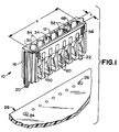
- FIG. 1 is an exploded perspective view of the strain relief structure of the subject invention and an associated circuit board.
- FIG. 2 is a top plan view of the strain relief structure.
- FIG. 3 is a front elevational view of the strain relief structure.
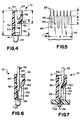
- FIG. 4 is a cross-sectional view taken along line 4-4 in FIG. 3.
- FIG. 5 is a top plan view of a flat flexible cable prepared for insertion into the strain relief structure of the subject invention.
- FIG. 6 is a cross-sectional view similar to FIG. 4 but showing a cable mounted in a first relative position in the strain relief structure.
- FIG. 7 is a cross-sectional view similar to FIGS. 4 and 6 but showing the cable fully inserted in the strain relief structure and mounted to a circuit board.
- the strain relief structure of the subject invention is identified generally by the numeral 10 in FIGS. 1-4.
- the strain relief structure 10 is unitarily molded from a plastics material and comprises a top surface 12 and a bottom board mounting surface 14.
- Opposed end walls 16 and 18 extend between the top and bottom surfaces 12 and 14.
- the end walls 16 and 18 are characterized by mounting pegs 20 and 22 which extend beyond the bottom surface 14. Fins on the pegs 20 and 22 will deform to achieve interference fit with appropriately dimensioned apertures 24 and 26 in a printed circuit board 28 to permit secure mounting of the strain relief structure to the printed circuit board 28.
- the strain relief structure 10 further comprises a rear wall 30 which extends between the opposed top and bottom surfaces 12 and 14 of the strain relief structure 10 and between the opposed end walls 16 and 18 thereof.
- the front of the strain relief structure 10 is substantially open in the illustrated embodiment, as explained further herein.
- strain relief structures within the scope of this invention could include a closed front.
- a cable receiving aperture indicated generally by the number 34 extends into the top surface 12 of the strain relief structure 10 and toward the bottom board mounting surface 14 thereof.
- the cable receiving aperture 34 is specifically constructed and dimensioned to receive a flat flexible cable 36 having a plurality of substantially parallel conductive leads 38 disposed within a substantially flexible resilient insulation 40, as shown in FIG. 5.
- the cable receiving aperture 34 defines a length "a" slightly greater than the width "b" of the cable 36.
- the aperture 34 further defines a width "c" which is substantially greater than the thickness of the flat flexible cable 36.
- the cable 36 is prepared by stripping all insulation from the conductors 38 for a distance "d" from the end.
- the distance “d” is selected in accordance with the thickness of the circuit board 28 to which the cable 36 is to be terminated. In particular, the distance “d” is selected to ensure that the exposed end of each conductor 38 will extend a sufficient distance into through holes in the circuit board 28 to achieve electrical connection with conductive areas on the circuit board.
- the cable 36 is further prepared by stripping portions of the insulation 40 intermediate adjacent conductors 38 for a distance "e”.
- the flat flexible cable 36 is prepared to comprise a plurality of discrete insulated leads 42 extending a distance "e” from the uninsulated portions of the conductors 38.
- the discrete insulated leads 42 terminate at insulation webs 44 which, as explained below, define stops which help to control the amount of insertion of the cable 36 into the strain relief structure 10 illustrated herein.
- the long slot 46 in the cable 36 may be provided to accommodate a transverse support 48 which could be incorporated into a long strain relief structure to enhance structural support.
- the cable receiving aperture 34 of the strain relief structure 10 comprises a plurality of transverse walls 50 which extend orthogonally from the rear wall 30 and function to divide portions of the aperture 34 into cavities for receiving the discrete insulated leads 42 and the exposed conductors 38 of the cable 36.
- the distance between adjacent transverse walls 50 is selected to define cavities having a width "f" sufficient to receive the insulated leads 42 of the cable 36.
- Each transverse wall 50 is of stepped configuration and defines an upper shoulder 54 generally adjacent the rear wall 30 and the top surface 12 of the strain relief structure 10, and a lower shoulder 56 spaced further from the rear wall 30 and top surface 12.
- the stepped configuration of the transverse walls 50 enables first and second relative depths of insertion of the cable 36 into the aperture 34 as explained herein.
- the upper shoulder 54 defines a first depth of insertion for a cable disposed generally adjacent the rear wall 30 of the structure 10.
- the lower shoulder 56 defines a second and deeper depth of insertion for a cable rotated or translated toward the open front of the strain relief structure 10.
- the shoulders 54 and 56 are intended to engage the insulation webs 44 which define stops on the cable 36 as depicted in FIG. 5.
- the depth of insertion "g" into the strain relief structure 10 as defined by the distance between the upper shoulder 54 and the bottom 14 is approximately equal to the distance "d+e” from the insulation web or stop 44 on the cable 36 to the extreme end of the cable 36.
- the lower shoulder 56 is disposed closer to the bottom surface 14 to enable the exposed conductors 38 to extend sufficiently beyond the bottom surface 14 of the strain relief structure 10 for subsequent electrical connection to conductive areas on a circuit board.
- the distance "h" between the lower shoulder 56 and the bottom 14 of the strain relief structure 10 is substantially less than the distance "d+e" representing the distance between the insulation web 44 on the cable 36 and the extreme end of the cable 36.
- the open front of the strain relief structure 10 is characterized by deflectable fingers 60 which are cantilevered from the top 12 into each respective cavity 52.
- the fingers 60 are aligned at an angle of approximately 30° to the direction of insertion and terminate at points 62 which define the narrowest front-to-rear dimension of each cavity 52. More particularly, the distance "i" between the rear wall 30 and the point 62 on each finger 60 is less than the thickness of the discrete insulated portions 42 of the flat flexible cable 36.
- the distance "j" between the upper shoulder 54 and the point 62 on the finger 60 is less than the length "e” of the discrete insulated leads 42.
- the use of the strain relief structure 10 can be best illustrated with reference to FIGS. 5-7.
- the flat flexible cable 36 is stripped and prepared substantially as shown in FIG. 5.
- the prepared, end of the cable 36 is then inserted into the cable receiving aperture 34 of the strain relief structure 10 prior to mounting the strain relief structure 10 onto the circuit board 28, and typically prior to shipping the prepared cable 36 and strain relief structure 10 to a location for assembly onto a circuit board.
- the cable 36 is generally aligned parallel to and adjacent the rear wall 30 of the strain relief structure 10 during this initial insertion.
- the insulation web 44 on the cable 36 will be urged into abutment with the upper shoulder 54 to define an initial maximum depth of insertion.
- the exposed conductors 38 will lie substantially within the cavities 52. Any minor extension of the conductors 38 beyond the cavities 52 will be protected intermediate the mounting structures 20 and 22.
- the distance "j" between the upper shoulder 54 and the point 62 is less than the length "e" of the discrete insulated portions 42 on the cable 36.
- the point 62 of each finger 60 will grippingly engage the insulation 40 on the cable 36 to prevent unintended separation of the strain relief structure 10 from the cable 36 during periods of shipment or storage.
- the flat flexible cable 36 is advanced into the FIG. 7 orientation within the strain relief structure 10 at the location of the component assembly.
- the FIG. 7 orientation can be achieved either immediately prior to mounting the strain relief structure 10 onto the circuit board 28 or sometime after the mounting of the strain relief structure 10 onto the circuit board 28.
- the FIG. 7 orientation of the cable is achieved by merely rotating or displacing the cable 36 away from the rear wall 30 of the strain relief structure 10. This forward movement of the cable 36 enables the stops 44 thereof to clear the upper shoulder 54, thereby permitting further insertion of the cable 36 into the cable receiving aperture 34.
- the points 62 of the fingers 60 will continue their locking engagement with the insulation 40 on the cable 36, thereby preventing withdrawal of the cable 36 and providing the required strain relief.
- the depth of insertion of the cable 36 relative to the strain relief structure 10 and the circuit board 28 is controlled by engagement of the insulation web 44 on the cable 36 with the lower shoulders 56. Consequently, overinsertion of the cable 36 in the FIG. 7 orientation is positively prevented.
- the structure 10 can be mounted to a cable for protecting the exposed leads of the cable prior to mounting the cable and the strain relief structure to a circuit board.
- the structure 10 can be securely mounted to a cable in a first position during storage and shipment and subsequently can lockingly engage the cable in a second position to achieve adequate strain relief between the cable and a circuit board.
- the structure 10 prevents over-insertion of the cable in each of two alternate dispositions on the cable.
- the structure 10 ensures protection and alignment of the leads of a cable prior to mounting on a board and subsequently ensures proper alignment and strain relief connection of the cable to a circuit board.
- a strain relief structure for mounting to a flat flexible cable.
- the strain relief structure comprises a cable receiving aperture having a plurality of transverse walls to divide the aperture into separate cavities for receiving the prepared ends of the flat flexible cable.
- the transverse walls are of stepped configuration.
- the stepped configuration defines upper and lower shoulders for defining first and second depths of insertion of the cable into the strain relief structure.
- the first depth of insertion is selected to substantially enclose the stripped and exposed conductive leads of the cable for protecting the cable end during periods of shipment and storage.
- the lower shoulder defines a depth of insertion substantially corresponding to the depth required for connecting the lead to conductive areas on a circuit board.
- the strain relief structure further comprises at least one deflectable finger for engaging the insulation on the cable and providing necessary strain relief. The finger is disposed to engage the insulation both at the first and at the second relative depths of insertion.
Landscapes
- Coupling Device And Connection With Printed Circuit (AREA)
- Structures For Mounting Electric Components On Printed Circuit Boards (AREA)
- Multi-Conductor Connections (AREA)
Claims (9)
- Zugentlastungseinrichtung (10) zur Erzielung einer Zugentlastungsverbindung zwischen einem flexiblen Flachkabel (36) und einer Leiterplatte (28), wobei sich die Zugentlastungseinrichtung (10) zusammensetzt aus
einem Öffnungsteil (34) zur Aufnahme des Kabels,
einem Zugentlastungsteil (60,62), der mit dem Kabel (36) zur Verhinderung eines Entfernens des Kabels (36) aus der Zugentlastungseinrichtung (60,62) in Eingriff bringbar ist, und
einem ersten Einsetzsteuerteil (54), das eine erste Einsetztiefe des Kabels in die Zugentlastungseinrichtung (10) hinein definiert, dadurch gekennzeichnet, daß der erste Einsetzsteuerteil (54) so ausgebildet ist, daß ein wahlweises Lösen des Kabels (36) vom ersten Einsetzsteuerteil (54) ermöglicht ist, und
ein zweiter Einsetzsteuerteil (56) eine zweite Einsetztiefe des Kabels in die Zugentlastungseinrichtung hinein definiert. - Zugentlastungseinrichtung (10) nach Anspruch 1, bei der der erste und der zweite Einsetzsteuerteil (54,56) so angeordnet sind, daß sie mit dem Kabel (36) in Eingriff kommen, nachdem zumindest ein Bereich des Kabels (36) von dem Zugentlastungsteil (60,62) erfaßt worden ist.
- Zugentlastungseinrichtung nach Anspruch 2, bei der die Zugentlastungseinrichtung (10) zumindest eine sich durch die Zugentlastungseinrichtung hindurcherstreckende Kabelaufnahmeöffnung und zumindest einen auslenkbaren Finger (60) umfaßt, der sich in die Kabelaufnahmeöffnung (34) der Zugentlastungseinrichtung (10) für einen Eingriff mit der Isolierung (44) auf dem Kabel (36) hineinerstreckt.
- Zugentlastungseinrichtung (10) nach Anspruch 3, bei der sich der Finger (60) mit einem spitzen Winkel in die Kabelaufnahmeöffnung (34) hineinerstreckt.
- Zugentlastungseinrichtung nach Anspruch 4, bei der der Finger (60) an einem in der Kabelaufnahmeöffnung (34) gelegenen Punkt endet und der Punkt mit der Isolierung (44) auf dem Kabel (36) in Eingriff bringbar ist.
- Zugentlastungseinrichtung (10) nach einem beliebigen der Ansprüche 1 bis 5, zur Verwendung mit einem flexiblen Flachkabel (36) mit einer Anordnung paralleler Leiter (38), einer um die Leiter (38) herum angeordneten flexiblen Isolierung (40) und zwischen den Leitern (38) in der Anordnung angeordneten Isolierungsstegen (44), wobei ein Ende des Kabels (36) durch Entfernen von Bereichen der Isolierungsstege zwischen benachbarten Leitern (38) auf eine gewählte Länge (d) vom Ende des Kabels vorbehandelt ist, die Zugentlastungseinrichtung zumindest eine sich in die Öffnung (34) hineinerstreckende Querwand (50) umfaßt und die Querwand (50) zumindest einen ersten Einsetzsteuerteil (54) für einen Eingriff des Isolierungssteges (44) zwischen den Leitern (38) des Kabels (36) zur Definierung einer ersten Einsetztiefe des Kabels (36) in die Zugentlastungseinrichtung (10) hinein aufweist, wobei es die erste Einsetztiefe der Zugentlastungseinrichtung (10) ermöglicht, das Ende des Kabels (36) zu schützen, und wobei die zweite Einsetztiefe eine Verbindung des Kabels (36) mit der Leiterplatte (28) ermöglicht.
- Zugentlastungseinrichtung nach Anspruch 6, bei der die Querwand (50) eine abgestufte Form hat, der erste Einsetzsteuerteil eine erste Schulter (54) in der abgestuften Querwand (50) bildet, die abgestufte Querwand (50) ferner den zweiten, von einer zweiten Schulter (56) gebildeten Einsetzsteuerteil zum Steuern der zweiten Einsetztiefe umfaßt und die erste und die zweite Schulter (54,56) vom Zugentlastungsteil (60,62) in einem Abstand angeordnet sind, der kleiner ist als die gewählte Länge an dem Ende des Kabels (36), von der der Isolierungssteg (44) entfernt ist.
- Zugentlastungseinrichtung (10) nach Anspruch 7, bei der die erste Schulter (54) derart angeordnet ist, daß das Ende des Kabels (36) im wesentlichen in der Zugentlastungseinrichtung (10) eingeschlossen ist, wenn der Isolierungssteg (44) zwischen den Leitern (38) mit der ersten Schulter (54) in Eingriff steht.
- Zugentlastungseinrichtung nach Anspruch 7 oder 8, bei der die zweite Schulter (56) derart angeordnet ist, daß sich das Ende des Kabels (36) über die Zugentlastungseinrichtung (10) hinauserstreckt, wenn der Isolierungssteg (44) zwischen den Leitern (38) mit der zweiten Schulter (56) in Eingriff steht.
Applications Claiming Priority (2)
| Application Number | Priority Date | Filing Date | Title |
|---|---|---|---|
| US07/315,052 US4886942A (en) | 1989-02-24 | 1989-02-24 | Strain relief structure for connecting flat flexible cable to a circuit board |
| US315052 | 1989-02-24 |
Publications (2)
| Publication Number | Publication Date |
|---|---|
| EP0384591A1 EP0384591A1 (de) | 1990-08-29 |
| EP0384591B1 true EP0384591B1 (de) | 1995-05-03 |
Family
ID=23222670
Family Applications (1)
| Application Number | Title | Priority Date | Filing Date |
|---|---|---|---|
| EP90301055A Expired - Lifetime EP0384591B1 (de) | 1989-02-24 | 1990-02-01 | Zugentlastungseinrichtung |
Country Status (4)
| Country | Link |
|---|---|
| US (1) | US4886942A (de) |
| EP (1) | EP0384591B1 (de) |
| JP (1) | JPH0626155B2 (de) |
| DE (1) | DE69019029T2 (de) |
Families Citing this family (17)
| Publication number | Priority date | Publication date | Assignee | Title |
|---|---|---|---|---|
| US5007856A (en) * | 1989-12-21 | 1991-04-16 | Amp Incorporated | Housing for an electrical connection |
| US4955814A (en) * | 1989-12-26 | 1990-09-11 | Electro Rubber Limited | Electrical connector device |
| DE69103362T2 (de) * | 1990-09-05 | 1994-12-01 | Thomas & Betts Corp | Beförderungsschutz- und Einfügungsgerät für mehradrige Kabel. |
| DE4102541C1 (de) * | 1991-01-29 | 1992-03-19 | Karl Lumberg Gmbh & Co, 5885 Schalksmuehle, De | |
| US5158476A (en) * | 1992-01-24 | 1992-10-27 | Landis & Gyr Metering Inc. | Modular strain relief device for electrical connectors |
| US5344338A (en) * | 1992-03-04 | 1994-09-06 | Molex Incorporated | Strain relief structure for connecting flat flexible cable to a circuit board |
| US5358417A (en) * | 1993-08-27 | 1994-10-25 | The Whitaker Corporation | Surface mountable electrical connector |
| DE4409517A1 (de) * | 1994-03-19 | 1995-09-21 | Murrplastik Systemtechnik Gmbh | Zugentlastung für Leitungen |
| US5462451A (en) * | 1994-06-13 | 1995-10-31 | Yeh; Te-Hsin | Electrical connector |
| US5667390A (en) * | 1995-03-06 | 1997-09-16 | Hon Hai Precision Ind. Co., Ltd. | I/O card and its associated cable harness assembly |
| DE19646716B4 (de) * | 1996-11-12 | 2008-08-28 | Molex Inc., Lisle | Elektrischer Verbinder, insbesondere für Kraftfahrzeuge |
| US6000951A (en) * | 1997-03-18 | 1999-12-14 | Prince Corporation | Electrical ribbon wire connectors |
| US6454596B1 (en) | 1999-06-30 | 2002-09-24 | Fci Americas Technology, Inc. | Electrical conductor strain relief for a printed circuit board |
| CN205543387U (zh) * | 2016-03-31 | 2016-08-31 | 乐视控股(北京)有限公司 | 柔性扁平电缆插座 |
| US10608359B2 (en) * | 2016-12-16 | 2020-03-31 | Samsung Electronics Co., Ltd. | Connection structure between flat cable and electronic circuit board |
| US11312462B1 (en) | 2020-08-06 | 2022-04-26 | Brunswick Corporation | Cowlings for marine drives and latching devices for cowlings for marine drives |
| US11577809B1 (en) | 2020-08-06 | 2023-02-14 | Brunswick Corporation | Cowlings and latching assemblies for cowlings for marine drives |
Family Cites Families (18)
| Publication number | Priority date | Publication date | Assignee | Title |
|---|---|---|---|---|
| US4226494A (en) * | 1978-12-28 | 1980-10-07 | Amerace Corporation | Circuit panel connector |
| CA1022253A (en) * | 1975-10-06 | 1977-12-06 | Edwin C. Hardesty | Electrical connecting devices for terminating cords |
| JPS5311269A (en) * | 1976-07-17 | 1978-02-01 | Yoshizou Yamamoto | Safety device for driving mechanism |
| JPS5746632A (en) * | 1980-09-01 | 1982-03-17 | Tokyo Shibaura Electric Co | Power converter |
| US4385341A (en) * | 1981-03-19 | 1983-05-24 | Northern Telecom Limited | Strain relief member for flat flexible cables |
| US4444450A (en) * | 1982-01-28 | 1984-04-24 | Amp Incorporated | Flat transmission cable connector and housing therefor |
| JPS5958377U (ja) * | 1982-10-08 | 1984-04-16 | 古野電気株式会社 | レ−ダ性能監視装置 |
| JPS60130200A (ja) * | 1983-12-16 | 1985-07-11 | 北川工業株式会社 | リ−ド線保持具 |
| DE3400935A1 (de) * | 1984-01-12 | 1985-07-25 | Grote & Hartmann Gmbh & Co Kg, 5600 Wuppertal | Verbindungsanordnung |
| DE3405126C2 (de) * | 1984-02-14 | 1985-12-05 | Philips Patentverwaltung Gmbh, 2000 Hamburg | Zugentlastungsaufsatz für Mehrfach-, insbesondere Flachbandkabel |
| GB2170961B (en) * | 1985-01-11 | 1988-10-12 | Sumitomo Electric Industries | Terminal connector assembly for multiconductor cable |
| GB8607330D0 (en) * | 1986-03-25 | 1986-04-30 | Ashley Accessories Ltd | Electric cord grip |
| US4719321A (en) * | 1986-07-28 | 1988-01-12 | Methode Electronics, Inc. | Wire locator and strain relief device |
| DE3888993T2 (de) * | 1987-03-06 | 1994-10-13 | Raytheon Co | Vorrichtung zur Überwachung der Radarleistungsfähigkeit. |
| US4804342A (en) * | 1987-04-24 | 1989-02-14 | Amp Incorporated | Cable strain relief for modular connector |
| JP2742056B2 (ja) * | 1988-06-14 | 1998-04-22 | 富士通株式会社 | X線マスク |
| JPH022107A (ja) * | 1988-06-15 | 1990-01-08 | Nec Corp | シンクロトロン放射光露光装置 |
| JPH06331490A (ja) * | 1993-05-24 | 1994-12-02 | Chiyoda Corp | 漏洩検出器及び漏洩位置検出方法 |
-
1989
- 1989-02-24 US US07/315,052 patent/US4886942A/en not_active Expired - Fee Related
-
1990
- 1990-01-30 JP JP2020359A patent/JPH0626155B2/ja not_active Expired - Lifetime
- 1990-02-01 EP EP90301055A patent/EP0384591B1/de not_active Expired - Lifetime
- 1990-02-01 DE DE69019029T patent/DE69019029T2/de not_active Expired - Fee Related
Also Published As
| Publication number | Publication date |
|---|---|
| DE69019029T2 (de) | 1995-12-07 |
| US4886942A (en) | 1989-12-12 |
| DE69019029D1 (de) | 1995-06-08 |
| JPH0626155B2 (ja) | 1994-04-06 |
| EP0384591A1 (de) | 1990-08-29 |
| JPH02247986A (ja) | 1990-10-03 |
Similar Documents
| Publication | Publication Date | Title |
|---|---|---|
| EP0384591B1 (de) | Zugentlastungseinrichtung | |
| US5417590A (en) | Plug and socket electrical connector system | |
| EP0386742B1 (de) | Elektrischer Verbinder mit Buchsenkontakten verschiedener Grössen und Mittel zur Vermeidung von falschem Anschliessen | |
| JP2934829B2 (ja) | 改良された導線保持手段を有する電気コネクタ | |
| US5344338A (en) | Strain relief structure for connecting flat flexible cable to a circuit board | |
| US6033238A (en) | Ribbon cable connector with ground bus | |
| US5147228A (en) | Terminal having positive retention feature and method of using same | |
| EP0014037B1 (de) | Elektrischer Stecker für Flachkabel | |
| US6283793B1 (en) | Electrical connector system | |
| US6244887B1 (en) | Electrical connector assembly | |
| US4921439A (en) | Center wire trap terminal and connector | |
| EP0792529A1 (de) | Koaxialverbinder und dessen befestigungsmethode auf eine leiterplatte | |
| US5306177A (en) | Insulation displacement termination system for input-output electrical connector | |
| CA2508357C (en) | Flexible cable electrical connector | |
| HK40887A (en) | Insulation displacement contact latching terminal | |
| US6116952A (en) | Multipole waterproof connector | |
| NZ202407A (en) | Multicontact insulation displacement connector | |
| US4439001A (en) | IDC Socket connector | |
| EP0631351A2 (de) | Elektrischer Verbinder zur Verbindung eines Kabels mit einer Leiterplatte | |
| US4653828A (en) | Pin shroud with universal latch means | |
| EP0147080B1 (de) | Steckverbinder für ein koaxiales Bandkabel | |
| EP1039585A2 (de) | Anordnung von elektrischen Anschlüssen eines Verbinders | |
| US5980307A (en) | Strain relief system for holding cables to circuit boards | |
| EP0135988B1 (de) | Elektrischer Kontaktverbinder mit Aufnahmekontakt zur Anpassung an den eingesteckten Stift | |
| EP0856912B1 (de) | Elektrischer Schneidklemmverbinder für inline-Mehrfachleiter |
Legal Events
| Date | Code | Title | Description |
|---|---|---|---|
| PUAI | Public reference made under article 153(3) epc to a published international application that has entered the european phase |
Free format text: ORIGINAL CODE: 0009012 |
|
| AK | Designated contracting states |
Kind code of ref document: A1 Designated state(s): DE FR GB |
|
| 17P | Request for examination filed |
Effective date: 19910102 |
|
| 17Q | First examination report despatched |
Effective date: 19930517 |
|
| GRAA | (expected) grant |
Free format text: ORIGINAL CODE: 0009210 |
|
| AK | Designated contracting states |
Kind code of ref document: B1 Designated state(s): DE FR GB |
|
| REF | Corresponds to: |
Ref document number: 69019029 Country of ref document: DE Date of ref document: 19950608 |
|
| ET | Fr: translation filed | ||
| PLBE | No opposition filed within time limit |
Free format text: ORIGINAL CODE: 0009261 |
|
| STAA | Information on the status of an ep patent application or granted ep patent |
Free format text: STATUS: NO OPPOSITION FILED WITHIN TIME LIMIT |
|
| 26N | No opposition filed | ||
| PGFP | Annual fee paid to national office [announced via postgrant information from national office to epo] |
Ref country code: GB Payment date: 19990108 Year of fee payment: 10 |
|
| PGFP | Annual fee paid to national office [announced via postgrant information from national office to epo] |
Ref country code: FR Payment date: 19990204 Year of fee payment: 10 |
|
| PGFP | Annual fee paid to national office [announced via postgrant information from national office to epo] |
Ref country code: DE Payment date: 19990226 Year of fee payment: 10 |
|
| PG25 | Lapsed in a contracting state [announced via postgrant information from national office to epo] |
Ref country code: GB Free format text: LAPSE BECAUSE OF NON-PAYMENT OF DUE FEES Effective date: 20000201 |
|
| GBPC | Gb: european patent ceased through non-payment of renewal fee |
Effective date: 20000201 |
|
| PG25 | Lapsed in a contracting state [announced via postgrant information from national office to epo] |
Ref country code: FR Free format text: LAPSE BECAUSE OF NON-PAYMENT OF DUE FEES Effective date: 20001031 |
|
| PG25 | Lapsed in a contracting state [announced via postgrant information from national office to epo] |
Ref country code: DE Free format text: LAPSE BECAUSE OF NON-PAYMENT OF DUE FEES Effective date: 20001201 |
|
| REG | Reference to a national code |
Ref country code: FR Ref legal event code: ST |