EP0382948B1 - Supply pin rearrangement for an integrated circuit - Google Patents
Supply pin rearrangement for an integrated circuit Download PDFInfo
- Publication number
- EP0382948B1 EP0382948B1 EP89200352A EP89200352A EP0382948B1 EP 0382948 B1 EP0382948 B1 EP 0382948B1 EP 89200352 A EP89200352 A EP 89200352A EP 89200352 A EP89200352 A EP 89200352A EP 0382948 B1 EP0382948 B1 EP 0382948B1
- Authority
- EP
- European Patent Office
- Prior art keywords
- pins
- supply
- output
- pads
- integrated circuit
- Prior art date
- Legal status (The legal status is an assumption and is not a legal conclusion. Google has not performed a legal analysis and makes no representation as to the accuracy of the status listed.)
- Expired - Lifetime
Links
Images

Classifications
-
- H—ELECTRICITY
- H10—SEMICONDUCTOR DEVICES; ELECTRIC SOLID-STATE DEVICES NOT OTHERWISE PROVIDED FOR
- H10W—GENERIC PACKAGES, INTERCONNECTIONS, CONNECTORS OR OTHER CONSTRUCTIONAL DETAILS OF DEVICES COVERED BY CLASS H10
- H10W72/00—Interconnections or connectors in packages
-
- H—ELECTRICITY
- H10—SEMICONDUCTOR DEVICES; ELECTRIC SOLID-STATE DEVICES NOT OTHERWISE PROVIDED FOR
- H10W—GENERIC PACKAGES, INTERCONNECTIONS, CONNECTORS OR OTHER CONSTRUCTIONAL DETAILS OF DEVICES COVERED BY CLASS H10
- H10W44/00—Electrical arrangements for controlling or matching impedance
- H10W44/501—Inductive arrangements
-
- H—ELECTRICITY
- H10—SEMICONDUCTOR DEVICES; ELECTRIC SOLID-STATE DEVICES NOT OTHERWISE PROVIDED FOR
- H10W—GENERIC PACKAGES, INTERCONNECTIONS, CONNECTORS OR OTHER CONSTRUCTIONAL DETAILS OF DEVICES COVERED BY CLASS H10
- H10W70/00—Package substrates; Interposers; Redistribution layers [RDL]
- H10W70/40—Leadframes
- H10W70/475—Capacitors in combination with leadframes
-
- H—ELECTRICITY
- H10—SEMICONDUCTOR DEVICES; ELECTRIC SOLID-STATE DEVICES NOT OTHERWISE PROVIDED FOR
- H10W—GENERIC PACKAGES, INTERCONNECTIONS, CONNECTORS OR OTHER CONSTRUCTIONAL DETAILS OF DEVICES COVERED BY CLASS H10
- H10W72/00—Interconnections or connectors in packages
- H10W72/50—Bond wires
- H10W72/541—Dispositions of bond wires
- H10W72/5449—Dispositions of bond wires not being orthogonal to a side surface of the chip, e.g. fan-out arrangements
Definitions
- the invention relates to an integrated circuit being coupled to connection pins via conductive connections, among which connection pins there is at least one first supply pin for connection to a first supply voltage and at least one second supply pin for connection to a second supply voltage.
- Integrated circuits of this kind are widely known, for example in an encapsulated form, the connection pins extending beyond the encapsulation.
- I.C.'s e.g. microprocessors or memories, wherein the supply pins are located diametrically opposite to one another
- Philips Data Handbook IC10, 1987, page 103 showing the pinning diagram for a SRAM
- Philips Data Handbook IC14, 1987, page 322 showing the pinning diagram for a microcontroller.
- a smoothing capacitance according to common practice located between the first supply pin and the second supply pin, necessarily needs long wires to cover the distance between the supply pins located diametrically.
- the parasitic impedance of these wires diminishes the efficiency of the smoothing capacitance.
- such long wires are liable to act as antennae for receiving or transmitting disturbances interfering with the circuitry.
- an inductive loop comprising the chip, whereon the bonding pads for the bonding wires connected to the supply pins are located, the bonding wires and the supply pins themselves, has a considerable inductance because of its relatively large area. This causes the occurrence of inductive'voltage spikes on the chip's internal supply lines, which spikes may interfere with the operation of the integrated circuit.
- the series arrangement of a supply pin and an associated bonding wire has an electrical path length that is the longest possible in the conventional dual-in-line I.C. This causes the impedance thereof, in particular the inductance, to be the largest possible.
- connection pins are located along the circumference of the I.C.
- Two supply pins are provided at opposite sides of the I.C. Consequently, a smoothing capacitor connected between the supply pins creates a relatively large loop likewise.
- Other arrangements of connection pins may comprise connection pins arranged in a grid having more than two columns and more than two rows. Such a grid arrangement allows a large density of pins, which in particular is advantageous for I.C.'s that consume more power. Especially in high power-consumption environment, where currents and current changes are large, the operation may be limited by the above inductive effect.
- an object of the invention to provide an integrated circuit module as described in the introductory part of claim 1, and an integrated circuit chip according to the introductory part of claim 7 being less susceptible to said parasitic effects.
- an integrated circuit module according to the invention is characterized, by the characterizing part of claim 1.
- an integrated circuit chip is characterized by the characterizing part of claim 7. The inductance of the series arrangement of a supply pin and its associated conductive connection now is the lowest possible.
- EP 205728 A2 descibes an integrated circuit chip suitable for connection, two kinds of power supplies that are to used for operating the integrated circuit chip, and a ground which constitutes a source power supply which is common to the two power supplies are connected to the Input-output pins that are provided on the package for the chip.
- the input-output pins connected to the power supplies are adjacently arranged on both sides of the input-output pin that is connected to the ground. Consequently, the lengths of the power supply current loops that are formed between the power supply terminals and the ground terminal are designed to become short, and hence the high frequency radiation from the loops reduced accordingly.
- the area of the loop described herein above is further decreased considerably, thus minimizing the inductances.
- Another advantage of this supply pin arrangement is, that the associated bonding wires and supply pins conduct currents in an anti-parallel orientation. This causes the common effective inductance of this arrangement of supply pins and associated bonding wires to be less than half of the inductance of a single bonding wire due to a substantial cancellation electro-magnetic fields generated by the inductances of the neighbouring wires.
- An embodiment of an integrated circuit according to the invention is characterized, in that there are provided at least two first supply pins and at least two second supply pins.
- This architecture decreases the amplitude of disturbances at the chip's internal supply lines even more because the presence of at least two supply pins and wires per supply voltage reduces the current per supply path by at least a factor 2.
- a plurality of other circuitry may be interconnected to the output pins.
- Each of the other circuits and the interconnections thereto represent impedances. Therefore output pins for transmitting output signals to other circuitry usually carry more powerful signals than other pins.
- the output pins By arranging the output pins in the immediate proximity of said supply pins the distance between the chip and the output pins is only slightly greater than the distance between the chip and the supply pins. As a consequence the inductance of the relevant wires and the output pins is only slightly larger in magnitude. Moreover, the effects of large currents and rapid current changes have only small effect on the supply voltages at the supply pins, for the latter are well protected by their pairwise presence.
- connection pins further comprise control pins such as a clock-input, or a chip-enable, or a read-enable or a write-enable, or an output-enable or a program-enable, according to the invention, is characterized in that the control pins are located nearer to a predetermined supply pin than connection pins not being a supply pin or output pin.
- control pins such as clock pins and enable pins in the immediate proximity of the paired supply pins a core of pins has been created. The pins forming said core are present in almost all I.C.'s.
- Chip designers may therefore take such a core as a starting point for creating a circuit, which is less sensitive to inductive interferences and generates much less of such inductive voltage spikes. Extensions of circuits designed according to the invention are easily accomplished, for the locations of the bulk of the pins and therefore the main parts of the lay-out are predetermined. For memories in particular this way of designing has important advantages as the memory cell matrices differ only in size, but not in lay-out.
- the amplitudes of disturbing voltages caused by switching were lower by a factor 4 à 5 than in a memory conventionally supplied.
- FIG 1 an example of the pin arrangement of a conventional dual-in-line I.C. is shown.
- the Figure shows a SRAM I.C., comprising an integrated circuit chip 100 encapsulated within an encapsulation 112, that has been drawn partially for the sake of clarity.
- the chip 100 is provided with bonding pads such as 114 and 116, located near the edges of chip 100.
- the bonding pads shown are connected via conductive connections, e.g. bonding wires, such as 122 and 124, to the connection pins 1-24 extending beyond the encapsulation 112.
- the connection pins 1-24 and the bonding wires such as 122 and 124 couple the chip 100 to the external world.
- the chip 100 is supplied with a supply voltage V CC via supply pin 24 and bonding wire 124, and with a supply voltage GND via supply pin 12 and bonding wire 122.
- supply pins 12 and 24 are placed diametrically opposite to each other.
- Connection pins 9-11 and 13-17 are input/output pins for data transport.
- Connection pins 1-8, 19, 22 and 23 are address pins.
- Connections 18, 20, and 21 serve as control pins for controlling the chip 100 with a chip-select signal, an output-enable signal and a write-enable signal, respectively.
- the locations of the bonding pads correspond circumferentially with the locations of the connection pins 1-24.
- this set up the electrical path length of the supply arrangement comprising supply pin 12 and bonding wire 122, and supply pin 24 and bonding wire 124, is the longest possible among all series connections of a connection pin and its associated bonding wire present.
- a smoothing capacitor 126 is connected between the supply pins 12 and 24.
- Another drawback of the conventional architecture emanates from the connection of this capacitor 26.
- the supply pins 12 and 24 are located diametrically opposite to each other the smoothing capacitor 26 has to be connected there-between by means of relatively long wires. This implies a presence of a loop of conductors, comprising the capacitor's 26 wires, the supply pins 12 and 24 and the bonding wires 122 and 124, the relatively large area thereof allowing further inductive effects, interfering the operation of the I.C. or with other circuitry in the I.C.'s neighbourhood (not shown). Also, the long wires' impedance may cause delays, thereby reducing the capacitor's 26 effect.
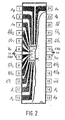
- FIG. 2 the pin arrangement of an I.C. according to the invention is presented by way of an example.
- the Figure shows a SRAM I.C., comprising an integrated circuit chip 300 encapsulated within an encapsulation 312, that has been drawn only partially for clarity.
- the chip 300 is provided with bonding pads, such as 314 and 316, that are located near the edges of chip 300.
- the bonding pads are connected via bonding wires, such as 322 and 324, to the connection pins 1-24, extending beyond the encapsulation 312.
- the chip 300 is supplied with a supply voltage V CC via supply pins 6 and 18, and with a supply voltage GND via supply pins 7 and 19.
- the supply pins 6 and 7 (and 18 and 19) now are disposed in such a manner as to minimize the respective aggregated electrial path length of the respective supply pin and its associated bonding wire.
- the supply pins 6 and 7 on the one hand and the supply pins 18 and 19 on the other hand are located centrally within their associated sequencies of connection pins.
- the aggregated inductance of the series arrangement of a supply pin and its associated bonding wire is reduced considerably with respect to the aggregated inductance present in the corresponding supply pin and bonding wire of the conventionally pinned I.C. of the previous Figure.
- a smoothing capacitor 326 (328) can be connected there-between using very short connecting wires.
- the loop, formed by the two supply pins 6 and 7, the bonding wires 322 and 324, chip 300 and capacitor 326 now has an extremely short circumference and an extremely small area enclosed thereby.
- the wires now connecting capacitor 326 (328) to the supply pins have a much smaller impedance than in the case shown in Figure 1, which increases the capacitor's effect.
- the area of said loop is much smaller than in the case of the previous Figure, which implies a much smaller loop-inductance, and therefore a much lower susceptibility to e.g. externally generated electromagnetic fields.
- the smoothing capacitor 326 e.g. a surface mounted device
- Another advantage of the supply pin arrangement having a V CC -pin in the immediate proximity of a GND-pin is the reduction of the effective aggregated inductances of the supply pins and the associated bonding wires. This reduction is caused by the anti-parallel orientation of the currents conducted in the conductors each comprising a supply pin and an associated bonding wire.
- the mutual inductance generated by anti-parallel oriented currents in two conductors disposed parallel to each other causes the effective inductance of the parallel arranged conductors to be less than half of the inductance of a single conductor.
- the shown I.C. further is provided with two supply pins 6 and 18 for supply voltage V CC and two supply pins 7 and 19 for supply voltage GND.
- the current conducted per supply pin now is halved with respect to the case shown in Figure 1, which further reduces the amplitude of inductive voltage spikes.
- V CC pins 6 and 18 and of the GND pins 7 and 19 are chosen to be rotationally symmetrical as can be seen from the drawing.
- a mirror-symmetrical arrangement of the supply pins could lead to the destruction of the I.C. in case it would unintentionally be inserted into a circuit board the other way around, that is in the drawing upside down.
- output pins 5, 8, 17 and 20 are located next to a supply pin. Said output pins are externally accessible terminals, coupled to outputs of the on-chip output buffers (not shown).
- the arrangement of output pins next to supply pins has several advantages. First, the length of the electrical path constituted by an output pin and its associated bonding wire is in the same order of magnitude as, or equal to, the length of the electrical path constituted by a supply pin and its associated bonding wire. Consequently, the impedance (inductance) of the former is equally low. Second, the output buffers are located in the margin of chip 300.
- the buffers are supplied via short on-chip supply lines (not shown). Short supply lines are advantageous for output buffers in particular, since they generally switch large current that may cause inductive voltage spikes on the associated supply lines. If the supply lines are kept as short as possible, the inductance thereof will be equally low.
- the control pin 10 for the chip-select signal, the control pin 15 for the write-enable signal and the control pin 22 for the output-enable are disposed beyond the output pins in their associated sequences of connection pins.
- the set of supply pins 6, 7, 18, 19, the output pins 4, 5, 8, 9, 16, 17, 20, 21 and the control pins 10, 15, 22 forms a core of frequently occurring pins in a memory I.C.
- I.C. for another type of I.C., for instance a microcontroller, another set of control pins may be arranged as the specific application of the I.C. may require.
- the concentration of said supply pins, output pins and control pins into a core, and dividing the chip into core circuitry and additional circuitry, has several advantages.
- the I.C. is less sensitive to inductive voltage spikes as already has been discussed herein above.
- the core of standard connection pins offers a starting point for I.C.-designers that is common to various lay-outs and from whereon extensions are relatively easy to make
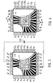
- connection pin arrangement for a conventional memory I.C. having connection pins located along its circumference.
- the I.C. comprises an integrated circuit chip 500 encapsulated within encapsulation 512, which has been drawn only partially for clarity.
- the chip 500 is provided with bonding pads such as 514 and 516, located near the chip's 500 edges.
- the bonding pads are connected to the connection pins, such as 14 and 28 via bonding wires, such as 522 and 524.
- Connection pins 28 and 14 are supply pins for receiving supply voltages V CC and GND, respectively.
- Connection pins 1, 10, 15 and 21 are not connected.
- Connection pins 11-13 and 16-20 are output pins, connections 2-9, 26 and 27 are address pins and connection pins 22-24 are control pins for receiving various chip-enable signals, which are included for the ease of memory expansion.
- the supply pins 14 and 28 have not the best possible location in view of the reduction of inductive interferences. First, they are not the shortest possible connection pins, for pins 1 and 15 are shorther but are not connected. Second, the supply pins are located on opposite sides of the I.C. Smoothing capacitor 526 is to be connected between the supply pins 28 and 14 using wires that bridge the long distance across the I.C. What has been further described with reference to the I.C. of Figure 1 with regard to the drawbacks of the pin arrangement will apply equally to the I.C. of Figure 3.
- FIG 4 an example of the pin arrangement for an I.C. having its pins disposed circumferentially is shown.
- the Figure shows an integrated circuit chip 600 within an encapsulation 612.
- the V DD supply pins 14 and 28 now are located next to a GND supply pin 15 and 1, respectively.
- the arrangement of a V DD supply pin next to a GND supply pin is located centrally in a relevant sequence of connection pins, that is, the arrangement is flanked by other connection pins on both sides, the number of other connection pins being approximately equal for both sides.
- Smoothing capacitors 626 and 628 have been connected between supply pins 14 and 15 and supply pins 1 and 28, respectively, via short wires.
- the output pins 12, 13 and 16, 17 are disposed next to the arrangement of supply pins 14 and 15.
- the output pins 3, 2 and 27, 26 are disposed next to the arrangement of supply pins 1 and 28.
- the connection pins 22-25 constitute the control pins for various chip-enable signals, the connection pins 5-11, 20
- pin-arrangements could be made for other kind of circuits, e.g. microcontrollers.
- similar arrangements are possible for integrated circuit modules comprising more than a single chip, which pin-arrangements similarly reflect the object of the invention to reduce the inductive voltage spikes by pairing the supply pins in the nearest proximity of the chips, and by disposing output pins next to the supply pins in the respective connection pin-arrangements.
Landscapes
- Semiconductor Integrated Circuits (AREA)
- Lead Frames For Integrated Circuits (AREA)
- Dram (AREA)
- Static Random-Access Memory (AREA)
- Semiconductor Memories (AREA)
Description
Claims (10)
- An integrated circuit module comprisingcharacterized in that the external connection pins comprise output pins (5,8), and the integrated circuit chip (300) comprises respective output buffers connected to output pins for supplying respective output signals, a respective one of the output pins being located next to each of the first and second supply pins.an integrated circuit chip (300) comprising a memory matrix;a plurality of external connection pins (1, 2, ..., 24), comprising at least a first supply voltage pin for connection to a first supply voltage (Vcc) and a second supply voltage pin (7) for connection to a second supply voltage (GND) different from the first supply voltage (Vcc), the first supply pin and the second supply pin being located adjacent one another;a plurality of conductive connections (322, 324, ...) coupling the integrated circuit chip (300) to the external connection pins (1, 2, ..., 24), an aggregate electrical path length of each of said supply pins and the respective conductive connection between the integrated circuit chip and the supply pin being equal to or shorter than an aggregate electrical path length of any of the connection pins, not being a supply pin, and the respective conductive connection between the circuit and the relevant connection pin not being a supply pin;
- The integrated circuit module of claim 1, wherein the connection pins comprise a third supply pin (18) for connection to the first supply voltage (Vcc) and a fourth supply pin (19) for connection to the second supply voltage (GND), the third and fourth supply pins (18,19) being located. adjacent one another, the first and second supply pins being located at one side of the integrated circuit and the third and fourth supply pins being located at an opposite side of the integrated circuit, respective ones the output pins (17,20) being located next to each of the third and fourth supply pins (18,19).
- An integrated circuit module according to Claim 1, wherein the external connection pins are arranged in at least a sequence of connection pins, the first and second supply pins being located next to each other and substantially centrally in the sequence; the integrated circuit chip (300) having a series of bonding pads (314, 316) located adjacent to the sequence of connection pins, each respective one of the connection pins being connected to a respective one of the bonding pads via a respective one of the bonding wires (322, 324); the bonding pads comprising a first and second supply pad connected to the first and second supply pin respectively, the first and second supply pads being located next to each other centrally in the series; a first and a second output pad being located next to the first and second supply pad respectively, the first and second output pad being connected to the output pins located next to the first and second supply pins respectively.
- An integrated circuit module according to claim 3, the external connection pins being arranged in at least the sequence of connection pins and a further sequence of connection pins, the integrated circuit chip being located between said sequence and said further sequence; the connection pins comprising a third and fourth supply pin (18,19) located next each other centrally in said further sequence, the third and fourth supply pin (18,19) being for connection to the first and second supply voltages, respectively; the integrated circuit chip (300) having a further series of bonding pads located adjacent to the further sequence of connection pins, the further series of bonding pads comprising is a third and fourth supply pad connected to the third and fourth supply pin respectively, the third and fourth supply pad being located next to one another in the further series; a third and fourth output pad being located next to the third and fourth supply pad respectively, the third and fourth output pad being connected to output pins located next to the third and fourth supply pins respectively.
- An integrated circuit module according to claim 1, 2, 3 or 4 wherein the connection pins further comprise control pins (10, 15, 22), such as a clock-input, or a chip-enable, or a write-enable, or a read-enable, or an output-enable, or a program-enable; the external connection pins being arranged in at least a sequence, the sequence comprising the first and second supply pins, at least some of the output pins and the control pins, no control pin being located in the sequence between any of the output pins and the supply pins.
- An integrated circuit module according to claim 5, the sequence comprising a core of connection pins, comprising all of the control pins, output pins and supply pins, the sequence comprising address pins, each located in the sequence outside said core.
- An integrated circuit chip comprising a memory matrix having a series of bonding pads for connection to connection pins, wherein the bonding pads comprise a first supply pad (316) for receiving a first supply voltage (Vcc), a second supply pad (314) for receiving a second supply voltage (GND) different from the first supply voltage; the first and second supply pads being located next to each other in the series; characterized in that the series of bonding pads contains output pads, the integrated circuit chip comprising output buffers coupled to respective ones of the output pads for supplying output signals, a respective one of the output pads being located in the series next to each of the first and second supply pads.
- An integrated circuit chip according to claim 7, comprising a further series of bonding pads, the series and the further series being located at opposite sides of the substrate, the further series of bonding pads comprising a third and fourth supply pad located next to each other, for receiving the first and second supply voltage respectively, the series of bonding pads containing further output pads, the integrated circuit chip comprising further output buffers coupled to respective ones of the further output pads, respective ones of the further output pads being located in the further series next to each of the third and fourth supply pads.
- An integrated circuit chip according to claim 7or 8, wherein the bonding padsfurther comprise control pads, such as a clock-input, or a chip-enable, or a write-enable, or a read-enable, or an output-enable, or a program-enable; the control pads being located in the series of control pads, no control pad being located in the series between any of the output pads and the supply pads. or
- An integrated circuit chip according to claim 7, 8 or 9, the series comprising a core of connection pads, comprising a1l of the control pads, output pads and supply pads, the series comprising address pads, each located in the series outside said core.
Priority Applications (13)
| Application Number | Priority Date | Filing Date | Title |
|---|---|---|---|
| DE68929487T DE68929487T2 (en) | 1989-02-14 | 1989-02-14 | Supply pin arrangement for an integrated circuit |
| ES89200352T ES2208631T3 (en) | 1989-02-14 | 1989-02-14 | PROVISION OF POWER PLUGS FOR AN INTEGRATED CIRCUIT. |
| EP01202742A EP1179848A3 (en) | 1989-02-14 | 1989-02-14 | Supply pin rearrangement for an I.C. |
| EP89200352A EP0382948B1 (en) | 1989-02-14 | 1989-02-14 | Supply pin rearrangement for an integrated circuit |
| JP2028142A JP2885456B2 (en) | 1989-02-14 | 1990-02-07 | Power supply pin layout for integrated circuits |
| SK649-90A SK278712B6 (en) | 1989-02-14 | 1990-02-09 | INTEGRATED CIRCUIT ON SEMICONDUCTOR SUBSTRATE |
| FI900653A FI113908B (en) | 1989-02-14 | 1990-02-09 | Arrangement of supply pins for an integrated circuit module and an integrated circuit chip |
| CS90649A CZ281891B6 (en) | 1989-02-14 | 1990-02-09 | Arrangement of integrated circuit on a semiconductor substrate |
| CN90101465A CN1025904C (en) | 1989-02-14 | 1990-02-12 | Supply pin rearrangement for IC |
| SU904743167A RU2092932C1 (en) | 1989-02-14 | 1990-02-12 | Integrated circuit on semiconductor substrate |
| KR1019900001770A KR100218076B1 (en) | 1989-02-14 | 1990-02-14 | Integrated Circuit Modules and Semiconductor Boards |
| MYPI90000244A MY105266A (en) | 1989-02-14 | 1990-02-14 | Supply pin rearrangement for an i.c. |
| US07/739,625 US5126822A (en) | 1989-02-14 | 1991-08-02 | Supply pin rearrangement for an I.C. |
Applications Claiming Priority (1)
| Application Number | Priority Date | Filing Date | Title |
|---|---|---|---|
| EP89200352A EP0382948B1 (en) | 1989-02-14 | 1989-02-14 | Supply pin rearrangement for an integrated circuit |
Related Child Applications (1)
| Application Number | Title | Priority Date | Filing Date |
|---|---|---|---|
| EP01202742.1 Division-Into | 2001-07-18 |
Publications (2)
| Publication Number | Publication Date |
|---|---|
| EP0382948A1 EP0382948A1 (en) | 1990-08-22 |
| EP0382948B1 true EP0382948B1 (en) | 2003-10-08 |
Family
ID=8202322
Family Applications (2)
| Application Number | Title | Priority Date | Filing Date |
|---|---|---|---|
| EP01202742A Withdrawn EP1179848A3 (en) | 1989-02-14 | 1989-02-14 | Supply pin rearrangement for an I.C. |
| EP89200352A Expired - Lifetime EP0382948B1 (en) | 1989-02-14 | 1989-02-14 | Supply pin rearrangement for an integrated circuit |
Family Applications Before (1)
| Application Number | Title | Priority Date | Filing Date |
|---|---|---|---|
| EP01202742A Withdrawn EP1179848A3 (en) | 1989-02-14 | 1989-02-14 | Supply pin rearrangement for an I.C. |
Country Status (11)
| Country | Link |
|---|---|
| EP (2) | EP1179848A3 (en) |
| JP (1) | JP2885456B2 (en) |
| KR (1) | KR100218076B1 (en) |
| CN (1) | CN1025904C (en) |
| CZ (1) | CZ281891B6 (en) |
| DE (1) | DE68929487T2 (en) |
| ES (1) | ES2208631T3 (en) |
| FI (1) | FI113908B (en) |
| MY (1) | MY105266A (en) |
| RU (1) | RU2092932C1 (en) |
| SK (1) | SK278712B6 (en) |
Cited By (1)
| Publication number | Priority date | Publication date | Assignee | Title |
|---|---|---|---|---|
| EP1179848A2 (en) * | 1989-02-14 | 2002-02-13 | Koninklijke Philips Electronics N.V. | Supply pin rearrangement for an I.C. |
Families Citing this family (7)
| Publication number | Priority date | Publication date | Assignee | Title |
|---|---|---|---|---|
| US5291455A (en) * | 1992-05-08 | 1994-03-01 | Motorola, Inc. | Memory having distributed reference and bias voltages |
| US5270964A (en) * | 1992-05-19 | 1993-12-14 | Sun Microsystems, Inc. | Single in-line memory module |
| WO1995022839A1 (en) * | 1994-02-17 | 1995-08-24 | National Semiconductor Corporation | Packaged integrated circuit with reduced electromagnetic interference |
| DE69620859T2 (en) * | 1996-01-22 | 2002-10-31 | Telefonaktiebolaget Lm Ericsson, Stockholm | Earth-symmetrical semiconductor integrated arrangement with a parallel resonance circuit |
| CN101505162A (en) * | 2007-12-21 | 2009-08-12 | 北京登合科技有限公司 | Wireless local area network module for mobile terminal |
| US7969002B2 (en) * | 2008-10-29 | 2011-06-28 | Maxim Integrated Products, Inc. | Integrated circuit packages incorporating an inductor and methods |
| CN102368686B (en) * | 2011-08-01 | 2016-08-10 | 刘圣平 | The circuit module port method for arranging that a kind of anti-short circuit is out of control |
Family Cites Families (9)
| Publication number | Priority date | Publication date | Assignee | Title |
|---|---|---|---|---|
| US3808475A (en) * | 1972-07-10 | 1974-04-30 | Amdahl Corp | Lsi chip construction and method |
| JPS5844743A (en) * | 1981-09-10 | 1983-03-15 | Fujitsu Ltd | Semiconductor integrated circuit |
| JPS58124262A (en) * | 1982-01-20 | 1983-07-23 | Nec Corp | Integrated circuit device |
| JPS601856A (en) * | 1983-06-20 | 1985-01-08 | Nec Corp | Memory chip module |
| JPS60152039A (en) * | 1984-01-20 | 1985-08-10 | Toshiba Corp | Gaas gate array integrated circuit |
| JPS61288451A (en) * | 1985-06-17 | 1986-12-18 | Toshiba Corp | Arrangement structure for input/output pin of ic package |
| JPS6281743A (en) * | 1985-10-07 | 1987-04-15 | Hitachi Comput Eng Corp Ltd | semiconductor equipment |
| JPS6290956A (en) * | 1985-10-17 | 1987-04-25 | Sumitomo Electric Ind Ltd | Semiconductor integrated circuit |
| EP1179848A3 (en) * | 1989-02-14 | 2005-03-09 | Koninklijke Philips Electronics N.V. | Supply pin rearrangement for an I.C. |
-
1989
- 1989-02-14 EP EP01202742A patent/EP1179848A3/en not_active Withdrawn
- 1989-02-14 ES ES89200352T patent/ES2208631T3/en not_active Expired - Lifetime
- 1989-02-14 EP EP89200352A patent/EP0382948B1/en not_active Expired - Lifetime
- 1989-02-14 DE DE68929487T patent/DE68929487T2/en not_active Expired - Lifetime
-
1990
- 1990-02-07 JP JP2028142A patent/JP2885456B2/en not_active Expired - Lifetime
- 1990-02-09 SK SK649-90A patent/SK278712B6/en not_active IP Right Cessation
- 1990-02-09 FI FI900653A patent/FI113908B/en active IP Right Grant
- 1990-02-09 CZ CS90649A patent/CZ281891B6/en not_active IP Right Cessation
- 1990-02-12 CN CN90101465A patent/CN1025904C/en not_active Expired - Lifetime
- 1990-02-12 RU SU904743167A patent/RU2092932C1/en active
- 1990-02-14 MY MYPI90000244A patent/MY105266A/en unknown
- 1990-02-14 KR KR1019900001770A patent/KR100218076B1/en not_active Expired - Lifetime
Cited By (1)
| Publication number | Priority date | Publication date | Assignee | Title |
|---|---|---|---|---|
| EP1179848A2 (en) * | 1989-02-14 | 2002-02-13 | Koninklijke Philips Electronics N.V. | Supply pin rearrangement for an I.C. |
Also Published As
| Publication number | Publication date |
|---|---|
| CN1045486A (en) | 1990-09-19 |
| FI113908B (en) | 2004-06-30 |
| MY105266A (en) | 1994-09-30 |
| JP2885456B2 (en) | 1999-04-26 |
| SK64990A3 (en) | 1998-01-14 |
| KR100218076B1 (en) | 1999-09-01 |
| DE68929487D1 (en) | 2003-11-13 |
| KR900013618A (en) | 1990-09-06 |
| EP1179848A3 (en) | 2005-03-09 |
| FI900653A0 (en) | 1990-02-09 |
| SK278712B6 (en) | 1998-01-14 |
| CZ64990A3 (en) | 1997-01-15 |
| DE68929487T2 (en) | 2004-07-22 |
| ES2208631T3 (en) | 2004-06-16 |
| EP0382948A1 (en) | 1990-08-22 |
| RU2092932C1 (en) | 1997-10-10 |
| CZ281891B6 (en) | 1997-03-12 |
| CN1025904C (en) | 1994-09-07 |
| JPH02277262A (en) | 1990-11-13 |
| EP1179848A2 (en) | 2002-02-13 |
Similar Documents
| Publication | Publication Date | Title |
|---|---|---|
| JP3530920B2 (en) | Multilayer package, packaging method, and multilayer packaged semiconductor device | |
| TW473751B (en) | Multi-layer capacitor, wiring board, and high-frequency circuit | |
| US6548757B1 (en) | Microelectronic device assemblies having a shielded input and methods for manufacturing and operating such microelectronic device assemblies | |
| US7420281B2 (en) | Stacked chip semiconductor device | |
| US5007025A (en) | Power and signal line bussing method for memory devices | |
| JPH05218285A (en) | Integrated-circuit chip package | |
| TW301050B (en) | ||
| EP1179848A2 (en) | Supply pin rearrangement for an I.C. | |
| WO1993004500A1 (en) | Distributed clock tree scheme in semiconductor packages | |
| TW567602B (en) | Multi-chip module | |
| US5126822A (en) | Supply pin rearrangement for an I.C. | |
| JP2009278051A (en) | Semiconductor package | |
| KR100800486B1 (en) | Semiconductor memory device having improved signal transmission path and driving method thereof | |
| WO2005045888A2 (en) | Electromagnetic noise shielding in semiconductor packages using caged interconnect structures | |
| TW486792B (en) | Ball grid array package semiconductor device having improved power line routing | |
| US7483248B1 (en) | Method and apparatus for detecting current changes in integrated circuits | |
| JPH1174449A (en) | Memory module | |
| JP3914649B2 (en) | Semiconductor device | |
| JP2002373940A (en) | Semiconductor integrated circuit device | |
| WO1995022839A1 (en) | Packaged integrated circuit with reduced electromagnetic interference | |
| US20210274642A1 (en) | Semiconductor apparatus | |
| US8549257B2 (en) | Area efficient arrangement of interface devices within an integrated circuit | |
| US7125743B2 (en) | Method for reduction of electromagnetic interference in integrated circuit packages | |
| JPS61288451A (en) | Arrangement structure for input/output pin of ic package | |
| US20050285281A1 (en) | Pad-limited integrated circuit |
Legal Events
| Date | Code | Title | Description |
|---|---|---|---|
| PUAI | Public reference made under article 153(3) epc to a published international application that has entered the european phase |
Free format text: ORIGINAL CODE: 0009012 |
|
| AK | Designated contracting states |
Kind code of ref document: A1 Designated state(s): CH DE ES FR GB IT LI NL SE |
|
| RIN1 | Information on inventor provided before grant (corrected) |
Inventor name: SALTERS, ROELOF HERMAN WILLEM Inventor name: PRINCE, BETTY |
|
| 17P | Request for examination filed |
Effective date: 19910219 |
|
| 17Q | First examination report despatched |
Effective date: 19921204 |
|
| APAB | Appeal dossier modified |
Free format text: ORIGINAL CODE: EPIDOS NOAPE |
|
| APAD | Appeal reference recorded |
Free format text: ORIGINAL CODE: EPIDOS REFNE |
|
| RAP3 | Party data changed (applicant data changed or rights of an application transferred) |
Owner name: KONINKLIJKE PHILIPS ELECTRONICS N.V. |
|
| APAD | Appeal reference recorded |
Free format text: ORIGINAL CODE: EPIDOS REFNE |
|
| APAB | Appeal dossier modified |
Free format text: ORIGINAL CODE: EPIDOS NOAPE |
|
| GRAG | Despatch of communication of intention to grant |
Free format text: ORIGINAL CODE: EPIDOS AGRA |
|
| GRAH | Despatch of communication of intention to grant a patent |
Free format text: ORIGINAL CODE: EPIDOS IGRA |
|
| GRAH | Despatch of communication of intention to grant a patent |
Free format text: ORIGINAL CODE: EPIDOS IGRA |
|
| GRAA | (expected) grant |
Free format text: ORIGINAL CODE: 0009210 |
|
| AK | Designated contracting states |
Kind code of ref document: B1 Designated state(s): CH DE ES FR GB IT LI NL SE |
|
| REG | Reference to a national code |
Ref country code: GB Ref legal event code: FG4D |
|
| REG | Reference to a national code |
Ref country code: CH Ref legal event code: EP |
|
| REF | Corresponds to: |
Ref document number: 68929487 Country of ref document: DE Date of ref document: 20031113 Kind code of ref document: P |
|
| REG | Reference to a national code |
Ref country code: SE Ref legal event code: TRGR |
|
| REG | Reference to a national code |
Ref country code: ES Ref legal event code: FG2A Ref document number: 2208631 Country of ref document: ES Kind code of ref document: T3 |
|
| ET | Fr: translation filed | ||
| PLBE | No opposition filed within time limit |
Free format text: ORIGINAL CODE: 0009261 |
|
| STAA | Information on the status of an ep patent application or granted ep patent |
Free format text: STATUS: NO OPPOSITION FILED WITHIN TIME LIMIT |
|
| 26N | No opposition filed |
Effective date: 20040709 |
|
| PG25 | Lapsed in a contracting state [announced via postgrant information from national office to epo] |
Ref country code: IT Free format text: LAPSE BECAUSE OF NON-PAYMENT OF DUE FEES;WARNING: LAPSES OF ITALIAN PATENTS WITH EFFECTIVE DATE BEFORE 2007 MAY HAVE OCCURRED AT ANY TIME BEFORE 2007. THE CORRECT EFFECTIVE DATE MAY BE DIFFERENT FROM THE ONE RECORDED. Effective date: 20050214 |
|
| APAH | Appeal reference modified |
Free format text: ORIGINAL CODE: EPIDOSCREFNO |
|
| REG | Reference to a national code |
Ref country code: GB Ref legal event code: 732E |
|
| REG | Reference to a national code |
Ref country code: GB Ref legal event code: 732E |
|
| REG | Reference to a national code |
Ref country code: FR Ref legal event code: TP |
|
| REG | Reference to a national code |
Ref country code: FR Ref legal event code: GC |
|
| PGFP | Annual fee paid to national office [announced via postgrant information from national office to epo] |
Ref country code: CH Payment date: 20080214 Year of fee payment: 20 Ref country code: ES Payment date: 20080324 Year of fee payment: 20 |
|
| PGRI | Patent reinstated in contracting state [announced from national office to epo] |
Ref country code: IT Effective date: 20080301 |
|
| PGFP | Annual fee paid to national office [announced via postgrant information from national office to epo] |
Ref country code: SE Payment date: 20080219 Year of fee payment: 20 Ref country code: GB Payment date: 20080213 Year of fee payment: 20 Ref country code: DE Payment date: 20080207 Year of fee payment: 20 Ref country code: NL Payment date: 20080203 Year of fee payment: 20 |
|
| PGFP | Annual fee paid to national office [announced via postgrant information from national office to epo] |
Ref country code: FR Payment date: 20080208 Year of fee payment: 20 |
|
| PGFP | Annual fee paid to national office [announced via postgrant information from national office to epo] |
Ref country code: IT Payment date: 20080226 Year of fee payment: 19 |
|
| REG | Reference to a national code |
Ref country code: CH Ref legal event code: PL |
|
| REG | Reference to a national code |
Ref country code: GB Ref legal event code: PE20 Expiry date: 20090213 |
|
| NLV7 | Nl: ceased due to reaching the maximum lifetime of a patent |
Effective date: 20090214 |
|
| EUG | Se: european patent has lapsed | ||
| REG | Reference to a national code |
Ref country code: ES Ref legal event code: FD2A Effective date: 20090216 |
|
| PG25 | Lapsed in a contracting state [announced via postgrant information from national office to epo] |
Ref country code: NL Free format text: LAPSE BECAUSE OF EXPIRATION OF PROTECTION Effective date: 20090214 |
|
| PG25 | Lapsed in a contracting state [announced via postgrant information from national office to epo] |
Ref country code: GB Free format text: LAPSE BECAUSE OF EXPIRATION OF PROTECTION Effective date: 20090213 |
|
| PG25 | Lapsed in a contracting state [announced via postgrant information from national office to epo] |
Ref country code: ES Free format text: LAPSE BECAUSE OF EXPIRATION OF PROTECTION Effective date: 20090216 |
|
| PGRI | Patent reinstated in contracting state [announced from national office to epo] |
Ref country code: IT Effective date: 20080301 |