EP0382151A2 - Sampling frequency down-converting apparatus and sampling frequency up-converting apparatus - Google Patents
Sampling frequency down-converting apparatus and sampling frequency up-converting apparatus Download PDFInfo
- Publication number
- EP0382151A2 EP0382151A2 EP90102267A EP90102267A EP0382151A2 EP 0382151 A2 EP0382151 A2 EP 0382151A2 EP 90102267 A EP90102267 A EP 90102267A EP 90102267 A EP90102267 A EP 90102267A EP 0382151 A2 EP0382151 A2 EP 0382151A2
- Authority
- EP
- European Patent Office
- Prior art keywords
- fsc
- sampling frequency
- frequency
- filter
- digital picture
- Prior art date
- Legal status (The legal status is an assumption and is not a legal conclusion. Google has not performed a legal analysis and makes no representation as to the accuracy of the status listed.)
- Granted
Links
Images


Classifications
-
- H—ELECTRICITY
- H04—ELECTRIC COMMUNICATION TECHNIQUE
- H04N—PICTORIAL COMMUNICATION, e.g. TELEVISION
- H04N9/00—Details of colour television systems
- H04N9/79—Processing of colour television signals in connection with recording
- H04N9/80—Transformation of the television signal for recording, e.g. modulation, frequency changing; Inverse transformation for playback
- H04N9/808—Transformation of the television signal for recording, e.g. modulation, frequency changing; Inverse transformation for playback involving pulse code modulation of the composite colour video-signal
- H04N9/8081—Transformation of the television signal for recording, e.g. modulation, frequency changing; Inverse transformation for playback involving pulse code modulation of the composite colour video-signal involving data reduction
-
- H—ELECTRICITY
- H04—ELECTRIC COMMUNICATION TECHNIQUE
- H04N—PICTORIAL COMMUNICATION, e.g. TELEVISION
- H04N11/00—Colour television systems
- H04N11/24—High-definition television systems
- H04N11/28—High-definition television systems involving bandwidth reduction, e.g. subsampling
-
- H—ELECTRICITY
- H04—ELECTRIC COMMUNICATION TECHNIQUE
- H04N—PICTORIAL COMMUNICATION, e.g. TELEVISION
- H04N19/00—Methods or arrangements for coding, decoding, compressing or decompressing digital video signals
- H04N19/50—Methods or arrangements for coding, decoding, compressing or decompressing digital video signals using predictive coding
- H04N19/59—Methods or arrangements for coding, decoding, compressing or decompressing digital video signals using predictive coding involving spatial sub-sampling or interpolation, e.g. alteration of picture size or resolution
-
- H—ELECTRICITY
- H04—ELECTRIC COMMUNICATION TECHNIQUE
- H04N—PICTORIAL COMMUNICATION, e.g. TELEVISION
- H04N9/00—Details of colour television systems
- H04N9/79—Processing of colour television signals in connection with recording
- H04N9/7904—Processing of colour television signals in connection with recording using intermediate digital signal processing
Definitions
- the present invention generally relates to a sampling frequency down-converting apparatus and a sampling frequency up-converting apparatus, which make it possible to effect recording operation on a recording medium as the digital signals of the comparatively low sampling frequencies or to effect transmission operations among the digital picture apparatuses in spite of the increase in the required frequency zone from the signals of the NTSC system (hereinafter referred to as NTSC signal) and the signal of the PAL system (hereinafter referred to as PAL signal), in the signals of systems called ATV (Advanced Television) system, HD - MAC (High Definition - Multiplexed Analogue Components) system and so on especially even among the television signals, namely, of the next generation television system which is designed so that the aspect ratio 3 : 4 of the NTSC system of the current television signal system or of the PAL system may be made as sideways long as 9 : 16, and the resolution may be improved.
- ATV Advanced Television
- HD - MAC High Definition - Multiplexed Analogue Components
- the NTSC signals only will be described hereinaf strictlyter now that the same things may be said even about the PAL signals.
- a digital picture apparatus such as a digital switcher handling the NTSC signals, a digital video tape recorder (hereinafter referred to as D - VTR) or the like
- the NTSC signals of the analog are sampled four times the color sub-carrier frequency Fsc, i.e., 4 Fsc.
- the sampling frequency becomes 4 Fsc ⁇ 14.3 MHz.
- the frequency zone of the NTSC signals to be digitalized is almost determined by a pre-low-pass filter (hereinafter referred to as LPF) provided on the input side of an A/D converter.
- LPF pre-low-pass filter
- the flat portion of the frequency characteristics of the LPF is to approximately 5.5 MNz from 0 (direct current). Since the required frequency zone of the NTSC signals is 4.2 MHz, the NTSC signals are digitalized with surplus by the sampling of 4 Fsc.
- An ACTV (Advanced Compatible Television) system is recently worth notice among an ATV system for improving the resolution with the aspect ratio of the above-described NTSC system some systems being made long sideways from 3 : 4 to 9 : 16, and some system.
- ACTV - E Advanced Compatible Television - Entry
- the frequency zone of the ACTV - E system increases by the oblong portion and the horizontal resolution improvement portion as compared with that of the NTSC system.
- the ACTV - E system finally requires the flat frequency zone of 7 MHz.
- the zone increases twice to effect the sequential scannings with respect to the interlace scanning of the ACTV - E system, thus resulting in 14 MHz.
- an essential object of the present invention is to provide an apparatus which provides affinity to the digital picture apparatus of the conventional 4 Fsc sampling, and may it possible to effect the sampling for satisfying the required frequency zone of the ACTV.
- the sampling frequency thins out the samples of the original digital picture signals eight times the color sub-carrier frequency so that the sampling frequency is converted into the intermediate digital picture signals about four times the color sub-carrier frequency. Also, in the sampling frequency up-converting apparatus of the present invention, the sampling frequency effects an interpolation among the samples of the intermediate digital picture signals about four times the color sub-carrier frequency so that the sampling frequency is high-pass converted into the original digital picture signals eight times the color sub-carrier frequency.
- FIG. 1 a block diagram in one embodiment of a sampling frequency down-converting apparatus in the present invention.
- An original digital picture signal which has sampled a signal (hereinafter referred to as ACTV - E signal) of the ACTV - E system by a 8 Fsc is inputted into a terminal 1.
- This signal is inputted into a band pass filter (hereinafter referred to as BPF 2) and also, is line shifted (is delayed by the number of the samples of 262H portion) by each 262H by two 262H delayers 3, 5.
- BPF 2 band pass filter
- the respective outputs are inputted into a LPF 4, a BPF 6.
- the respective outputs of the BPF 2, the LPF 4, the BPF 6 are added by an adder 8, and also, are delayed by one clock by a data latching circuit (D) 9.
- n clock n is a positive integer
- the adder 10 is added to the output of the data latching circuit 9 by the adder 10.
- the added output is delayed by one clock by the data latching circuit (D) 11.
- the addition output of the adder 10 or the delay output of the data latching circuit 11 is alternately selected for each field to output it (the output means of the FLD is not shown).
- the data latching circuits 7, 9, 11 provided so far are all latched by the clock of 8 Fsc from the terminal 16 (one sample is delayed by one clock).
- the output of the MUX 12 is inputted into the data latching circuit (D) 13 and is delayed by one clock by the clock of the 4 Fsc.
- the clock of the 4 Fsc makes the clock of 8 Fsc from the terminal 16 through the frequency division by the counter 17.
- the output of the data latching circuit 13, together with the clock of 4 Fsc of the terminal 15 as the intermediate digital picture signal of the sampling frequency of the approximately 4 Fsc, is outputted into the digital interface (not shown) from the terminal 14.
- the means for thinning out the original digital picture signals is composed of the data latching circuit 11, the MUX 12, the data latching circuit 13. It is to be noted that the clocks of 8 Fsc to be inputted into the 262H delayers 3, 5 and the BPFs 2, 6 and the LPF 4 are also the clocks from the terminal 16.
- the BPF 2 and BPF 6 are completely the same in construction.
- the detailed block diagram in one embodiment thereof is shown in Fig. 2.
- the data latching circuit (D) 21 is a circuit for delaying by one clock.
- the other data latching circuits (2D) 23, 25, 27, 29, 31, 33 are the circuits for delaying two clocks.
- the signals from the terminal 20 are shifted by these data latching circuits.
- the output of each data latching circuit is multiplied respectively by coefficients -1, 4, -7, 8, -7, 4, -1 by the coefficient multipliers 22, 24, 26, 28, 30, 32, 34. Seven outputs of these coefficient multipliers 22, 24, 26, 28, 30, 32, 34 are added by the adder 35 and are outputted into the terminal 36.
- FIG. 3 is a detailed block diagram in one embodiment of the LPF 4.
- the signals from the terminal 40 are shifted by the data latching circuits (2D) 42, 44, 46, 48, 50, 52, 54 which delay two clocks.
- the signal of the terminal 40 and the output of each data latching circuit is multiplied respectively by the coefficients 2, -3, -4, 37, 37, -4, -3, 2 by the coefficient multipliers 41, 43, 45, 47, 49, 51, 53, 55, and eight outputs of these coefficient multipliers 41, 43, 45, 47, 49, 51, 53, 55 are added by the adder 56 and are outputted into the terminal 57.
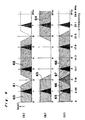
- Fig. 4 (a) through (c) are the frequency spectrum by the various types of samplings.
- the scale of the quadrature axis is shown in Fsc unit and MHz unit.
- FIG. 4 (a) shows a case where the sampling has been effected by the sampling frequency of 4 Fsc, wherein the zone of the analog ACTV signal to be sampled in advance by the LPF and so on before the analog/digital (A/D) conversion is effected is limited to 2 Fsc (7.16 MHz), thereafter the A/D conversion is effected, so that a Y signal component of base band spectrum 60 (oblique line portion surrounded in solid lines) containing a C signal component 61 around the color sub-carrier wave and a folded spectrum 62 (oblique line portion surrounded by dotted lines) around the 4 Fsc may not be overlapped with the 2 Fsc provided as the boundary.
- a Y signal component of base band spectrum 60 (oblique line portion surrounded in solid lines) containing a C signal component 61 around the color sub-carrier wave and a folded spectrum 62 (oblique line portion surrounded by dotted lines) around the 4 Fsc may not be over
- FIG. 4 (b) shows a case where the sampling has been effected by the sampling frequency of the 8 Fsc. Since the folded spectrum 64 around the 8 Fsc is sufficiently higher than the base band spectrum 63, the zone restriction is not required to be effected in advance as in the (a). The zone of the ACTV signal to be sampled may be extended over necessary 2 Fsc. Therefore, the flat frequency characteristics may be obtained till 2 Fsc, i.e., 7. 16 MHz as shown. Fig.
- the base band spectrum 66 and the folded spectrum 68 become the relation of the frequency interleaving just in the piled up region 67 if the sub-sampling frequency for obtaining the intermediate digital signal is shifted by Fh/2 or Fv/2 with respect to the 4 Fsc.
- the frequency characteristics may provide the flat ACTV signal as far as the 2 Fsc if the digital-along conversion (D/A) is effected after the signal has been restored to the original digital signal of the sampling frequency 8 Fsc through the interpolation of the thinned out samples.
- the color sub-carrier wave is selected into a proper frequency (odd times of one half of the fH), the C signal is modulated by the color sub-carrier wave to effect the frequency interleaving.
- the piled up region 67 is better not to be applied upon the zone of the C signal component 65.
- Fig. 5 shows a case of the sampling by the sampling frequency of the 8 Fsc.
- Fig. 5 (b) shows a case of the sampling by the sampling frequency of the 4 Fsc to be thinned out for every other sample from the (a).
- FIG. 5 (c) shows a case of a so-called line offset type, where one sample is shifted every other line in the thinning out method.
- Fig. 5 (d) is a case of a so-called field offset type, where one sample is shifted every other field in the thinning out method.
- the sampling frequency of (c) is shifted by fh/2 from the 4 Fsc, while the sampling frequency of the (d) is shifted by fv/2 from the 4 Fsc.
- sampling frequency down-converting apparatus in the present invention of Fig. 1 realizes the field offset type of Fig. 5 (d). Especially it is not restricted to this.
- a circuit from the terminal 1 to the output of the adder 10 is a so-called zone restricting filter.
- the sampling frequency of approximately 4 Fsc so as to become such a frequency spectrum as shown by Fig. 4 (c)
- the component of the folded spectrum 68 in the piled up region 67 is previously restricted in zone by the chasing filter of the Fv period only in only the passing zone of the BPF so that the component distribution is not be leaked into the component within the base band spectrum 66 separated by Fv/2.
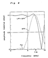
- the frequency characteristics of the zone restricting filter (composed of the terminal 1 through the adder 10) is shown in Fig. 6 in a case where the BPFs 2, 6 and the LPF 4 shown in Fig.
- Fig. 3 are used.
- the frequency characteristics shown in the dotted lines become the direct current (DC) in the 2 Fsc (7.16 MHz) of the central frequency, and zero in the Fsc.
- DC direct current
- the chasing filter in the passing zone of the BPF is omitted, since the filtering is effected at the fv period, which is difficult to illustrate.
- the envelope of the frequency characteristics of the chasing filter shape looks as if it is the frequency characteristics of the BPF shown in the dotted lines.
- the overall characteristics containing the LPF shown in the solid lines become the flat characteristics of approximately 1 dB from the DC to the 2 Fsc.
- the original signals sampled by the sampling frequency of the 8 Fsc are thinned out every other sample to generate the intermediate digital picture signal of approximately 4 Fsc in the sampling frequency.
- the field offset type is realized by the passing of the output of the data latching circuit 11 every other field in the MUX 12. If a circuit (which is composed of the terminal 1 through the adder 10) constituting the zone limiting filter is omitted here, the fundamental performance of sampling with the 4 Fsc the original digital signal sampled by the 8 Fsc in accordance with the present invention may be achieved.
- Fig. 7 is a block diagram in one embodiment of a sampling frequency up-converting apparatus in the present invention.
- the intermediate digital picture signal sub-sampled by the sampling frequency (sub-sampling frequency) of the approximately 4 Fsc is inputted into the terminal 70 through the digital interface (not shown).
- This signal is inputted into the BPF 71, and also, is inputted into the 262H delayer 72.
- the line shifting is effected for each 262H by two 262H delayers 72, 74 so as to input the respective outputs into the LPF 73, the BPF 75.
- the respective outputs of the BPF 71, LPF 73, BPF 75 are added into the adder 77, and also, are delayed by one clock by the data latching circuit (D) 78.
- An interpolating sample producing means is composed of the BPF 71, the 262H delayer 72, the LPF 73, the 262H delayer 74, the BPF 75 and the adder 77, the D 78.
- the output of the 262H delayer 72 is delayed by the n clock (n is a positive integer) for the timing adjustment by the n data latching circuit (nD) 76.
- the delay output and the output of the data latching circuit 78 are selected by a MUX 79.
- the data latching circuits 76, 78 provided so far are all latched (one sample is delayed by one clock) by the clock of 4 Fsc from the terminal 83. Since the selection of the MUX 79 is effected likewise by the clock (rate) of the 4 Fsc from the terminal 83, the output of the data latching circuit 78 and the output of the n data latching circuit 76 alternately appear at the rate of the 8 Fsc finally in the output of the MUX 79. It is inputted into the data latching circuit (D) 80 and is delayed by one clock by the clock of the 8 Fsc. The clock of the 4 Fsc is made twice by the PLL 84 to make this 8 Fsc clock.
- the interpolating sample filling means is composed of the MUX 79, the D 80. It is to be noted that the clocks of the 4 Fsc to be inputted into the 262H delayers 72, 74, the BPFs 71, 75 and the LPF 73 are the clocks from the terminal 83.
- the BPF 71 and the BPF 75 are completely the same in construction.
- the detailed block diagram in one embodiment thereof is shown in Fig. 8.
- the signal from the terminal 90 is shifted by the data latching circuits (D) 92, 94, 96, 98, 100, 102 for delaying one clock, and also, the signal of the terminal 90 and the output of each data latching circuit are multiplied by the same coefficients -1, 4, -7, 8, -7, 4, -1 as those of the coefficient multiplier shown in Fig.
- Fig. 9 is a detailed block diagram in one embodiment of a LPF 73. Since the same drawing is the same as Fig. 3 wherein the data latching circuit for delaying two clocks is changed into a latching circuit (D) for delaying one clock, the description thereof will be described.
- Fig. 10 shows as a model the operations of the 262H delayers 72, 74 of the sampling frequency up-converting apparatus shown in Fig. 7 and the respective filters 71, 73, 75.
- the (L + 262) line is the output of the BPF 75
- the (L - 262) line is the output of BPF 71
- the numeral shown on the sample " * " is the coefficient of the coefficient multiplier shown in Fig. 8.
- the (L) line is the output of the LPF 73, the numeral shown on the sample “ * “ is the coefficient of the coefficient multiplier shown in Fig. 9.
- the sample “ o " is the thinned out sample to be interpolated. The sample is multiplied by the coefficient shown on the sample “ * “ and the total sum of them is removed to interpolate the sample " o " .
- Such an original digital signal as shown in Fig. 5 (a) is provided by the alternate replacement by the output sample " * " of the n data latching circuit 76 in the MUX 79.
- the frequency characteristics of the BPF and the LPF of Fig. 7 are shown in Fig. 6 as shown in those of the BPF and the LPF of Fig. 1.
- the coefficients of the coefficient multipliers of the BPF and the LPF are set respectively -5, 16, -27, 32, -27, 16, -5, and 8, -10, -18, 148, 148, -18, -10, 8, the frequency characteristics are further improved and the circuit scale increases somewhat.
- the 8 Fsc sampling of the ACTV - E signal has been considered the original digital signal, but the sampling frequency of the 8 Fsc is too low, because the required zone becomes 14 MHz in the ACTV - 1 signal.
- the signal sampled by the sampling frequency of the 16 Fsc is to be the original digital picture signal. It is low-pass converted into the intermediate digital picture signal of approximately 8 Fsc by the thinning.out method (sub-sampling) of the field offset or the like. Also, the intermediate digital picture signal of the approximately 8 Fsc is restored into the original digital picture signal of the 16 Fsc by the interpolation.
- the digital interface provided between the digital picture apparatuses by the use of the intermediate digital signal of approximately 4 Fsc, with respect to the ACTV - E signal requiring the flat signal zone of the 7 MHz, so that most of the digital picture apparatuses including a digital VTR using the sampling frequency of the conventional 4 Fsc may be used as they are.
- the recording time and the format of the DVCR may be provided as in a case where the recording signal is the NTSC signal.
Abstract
Description
- The present invention generally relates to a sampling frequency down-converting apparatus and a sampling frequency up-converting apparatus, which make it possible to effect recording operation on a recording medium as the digital signals of the comparatively low sampling frequencies or to effect transmission operations among the digital picture apparatuses in spite of the increase in the required frequency zone from the signals of the NTSC system (hereinafter referred to as NTSC signal) and the signal of the PAL system (hereinafter referred to as PAL signal), in the signals of systems called ATV (Advanced Television) system, HD - MAC (High Definition - Multiplexed Analogue Components) system and so on especially even among the television signals, namely, of the next generation television system which is designed so that the aspect ratio 3 : 4 of the NTSC system of the current television signal system or of the PAL system may be made as sideways long as 9 : 16, and the resolution may be improved.
- The NTSC signals only will be described hereinafter now that the same things may be said even about the PAL signals. Generally, in a digital picture apparatus such as a digital switcher handling the NTSC signals, a digital video tape recorder (hereinafter referred to as D - VTR) or the like, the NTSC signals of the analog are sampled four times the color sub-carrier frequency Fsc, i.e., 4 Fsc.
- From Fsc ≒ 3.58 MHz, the sampling frequency becomes 4 Fsc ≒ 14.3 MHz. At this time, the frequency zone of the NTSC signals to be digitalized is almost determined by a pre-low-pass filter (hereinafter referred to as LPF) provided on the input side of an A/D converter. Normally, the flat portion of the frequency characteristics of the LPF is to approximately 5.5 MNz from 0 (direct current). Since the required frequency zone of the NTSC signals is 4.2 MHz, the NTSC signals are digitalized with surplus by the sampling of 4 Fsc.
- An ACTV (Advanced Compatible Television) system is recently worth notice among an ATV system for improving the resolution with the aspect ratio of the above-described NTSC system some systems being made long sideways from 3 : 4 to 9 : 16, and some system.
- The ACTV system only is described hereinafter now that the same thing can be said even about the other ATV system. In the ACTV system, the field frequency and the color sub-carrier frequency are the same as in the NTSC system. But in the horizontal scanning frequency, there are a case where there is 15.75 / 1.00 1 kHz as that of the NTSC system, and a case where there is 31.5 / 1.00 1 kHz which is twice 15.75 so as to effect 525 sequential scannings for each one field. The former is called ACTV - E (Advanced Compatible Television - Entry) system, while the latter is called ACTV - 1.
- The frequency zone of the ACTV - E system increases by the oblong portion and the horizontal resolution improvement portion as compared with that of the NTSC system. In order to have sideways long portion, the required frequency zone 4.2 MHz of the NTSC system increases as follows.
(16 / 9) / (4 / 3) X 4.2 MHz
= (4 / 3) X 4.2
= 5.6 MHz
In order to further improve the horizontal resolution as compared with that of the NTSC system, the ACTV - E system finally requires the flat frequency zone of 7 MHz. - Also, in the case of ACTV - 1 system, the zone increases twice to effect the sequential scannings with respect to the interlace scanning of the ACTV - E system, thus resulting in 14 MHz.
- In a case of digitalizing the signals (hereinafter referred to as ACTV signals) of such an ACTV system, in the sampling of the conventional 4 Fsc, the zone to be converted is approximately 5. 5 MHz as described hereinabove and is insufficient. Therefore, it is impossible to serve a double purpose the digital picture apparatus of the 4 Fsc sampling for the conventional NTSC system use, which is the original purpose of the ACTV system. Thus, conventionally it has been considered to increase the sampling frequency like 5 Fsc or 6 Fsc. But they are both in a direction of increasing the data rate. The D - VCR for recording them reduces the recording time as compared with the NTSC system in the recording operation on the recording medium of the same capacity. In our time of longer hours' image transcription, it is a big task to be solved for the D - VTR which records the signals in the next generation television system.
- Accordingly, an essential object of the present invention is to provide an apparatus which provides affinity to the digital picture apparatus of the conventional 4 Fsc sampling, and may it possible to effect the sampling for satisfying the required frequency zone of the ACTV.
- In accomplishing the above-described object, according to one preferred embodiment of the present invention, in the sampling frequency down-converting apparatus, the sampling frequency thins out the samples of the original digital picture signals eight times the color sub-carrier frequency so that the sampling frequency is converted into the intermediate digital picture signals about four times the color sub-carrier frequency. Also, in the sampling frequency up-converting apparatus of the present invention, the sampling frequency effects an interpolation among the samples of the intermediate digital picture signals about four times the color sub-carrier frequency so that the sampling frequency is high-pass converted into the original digital picture signals eight times the color sub-carrier frequency.
- These and other objects and features of the present invention will become apparent from the following description taken in conjunction with the preferred embodiment thereof with reference to the accompanying drawings, in which;
- Fig. 1 is a block diagram in one embodiment in a sampling frequency down-converting apparatus of the present invention;
- Fig. 2 is a detailed block diagram in one embodiment of a BPF of Fig. 1;
- Fig. 3 is a detailed block diagram in one embodiment of a LPF of Fig. 1;
- Fig. 4 shows a frequency spectrum in each type of sampling;
- Fig. 5 shows a two-dimensional model view of the various types of samplings;
- Fig. 6 shows a frequency characteristic graph of the BPF and LPF of Fig. 1;
- Fig. 7 is a block diagram in one embodiment in a sampling frequency up-converting apparatus of the present invention;
- Fig. 8 is a detailed block diagram in one embodiment of the BPF of Fig. 7;
- Fig. 9 is a detailed block diagram in one embodiment of the LPF of Fig. 7; and
- Fig. 10 is a model view for illustrating the interpolation processing.
- Before the description of the present invention proceeds, it is to be noted that like parts are designated by like reference numerals throughout the accompanying drawings.
- Referring now to the drawings, there is shown in Fig. 1, a block diagram in one embodiment of a sampling frequency down-converting apparatus in the present invention. An original digital picture signal which has sampled a signal (hereinafter referred to as ACTV - E signal) of the ACTV - E system by a 8 Fsc is inputted into a
terminal 1. This signal is inputted into a band pass filter (hereinafter referred to as BPF 2) and also, is line shifted (is delayed by the number of the samples of 262H portion) by each 262H by two262H delayers LPF 4, aBPF 6. Then, the respective outputs of theBPF 2, theLPF 4, theBPF 6 are added by anadder 8, and also, are delayed by one clock by a data latching circuit (D) 9. After the output of the262H delayer 3 has been delayed by n clock (n is a positive integer) for the timing adjustment by the n data latching circuit (nD), it is added to the output of the data latching circuit 9 by theadder 10. The added output is delayed by one clock by the data latching circuit (D) 11. In accordance with the field identification signal (FLD) for distinguishing two fields in one frame, the addition output of theadder 10 or the delay output of the data latching circuit 11 is alternately selected for each field to output it (the output means of the FLD is not shown). As shown in the same drawing, thedata latching circuits 7, 9, 11 provided so far are all latched by the clock of 8 Fsc from the terminal 16 (one sample is delayed by one clock). Then, the output of theMUX 12 is inputted into the data latching circuit (D) 13 and is delayed by one clock by the clock of the 4 Fsc. The clock of the 4 Fsc makes the clock of 8 Fsc from theterminal 16 through the frequency division by thecounter 17. The output of thedata latching circuit 13, together with the clock of 4 Fsc of theterminal 15 as the intermediate digital picture signal of the sampling frequency of the approximately 4 Fsc, is outputted into the digital interface (not shown) from theterminal 14. The means for thinning out the original digital picture signals is composed of the data latching circuit 11, theMUX 12, thedata latching circuit 13. It is to be noted that the clocks of 8 Fsc to be inputted into the262H delayers BPFs LPF 4 are also the clocks from theterminal 16. - The BPF 2 and BPF 6 are completely the same in construction. The detailed block diagram in one embodiment thereof is shown in Fig. 2. In Fig. 2, only the data latching circuit (D) 21 is a circuit for delaying by one clock. The other data latching circuits (2D) 23, 25, 27, 29, 31, 33 are the circuits for delaying two clocks. The signals from the
terminal 20 are shifted by these data latching circuits. The output of each data latching circuit is multiplied respectively by coefficients -1, 4, -7, 8, -7, 4, -1 by thecoefficient multipliers coefficient multipliers adder 35 and are outputted into the terminal 36. Also, Fig. 3 is a detailed block diagram in one embodiment of theLPF 4. In Fig. 3, the signals from the terminal 40 are shifted by the data latching circuits (2D) 42, 44, 46, 48, 50, 52, 54 which delay two clocks. Also, the signal of the terminal 40 and the output of each data latching circuit is multiplied respectively by thecoefficients 2, -3, -4, 37, 37, -4, -3, 2 by thecoefficient multipliers coefficient multipliers adder 56 and are outputted into the terminal 57. - The operation of the sampling frequency down-converting apparatus (see Fig. 1) composed of such BPF, LPF and so on will be illustrated by the use of Fig. 4, Fig. 5. Fig. 4 (a) through (c) are the frequency spectrum by the various types of samplings. The scale of the quadrature axis is shown in Fsc unit and MHz unit. Fig. 4 (a) shows a case where the sampling has been effected by the sampling frequency of 4 Fsc, wherein the zone of the analog ACTV signal to be sampled in advance by the LPF and so on before the analog/digital (A/D) conversion is effected is limited to 2 Fsc (7.16 MHz), thereafter the A/D conversion is effected, so that a Y signal component of base band spectrum 60 (oblique line portion surrounded in solid lines) containing a
C signal component 61 around the color sub-carrier wave and a folded spectrum 62 (oblique line portion surrounded by dotted lines) around the 4 Fsc may not be overlapped with the 2 Fsc provided as the boundary. Fig. 4 (b) shows a case where the sampling has been effected by the sampling frequency of the 8 Fsc. Since the foldedspectrum 64 around the 8 Fsc is sufficiently higher than thebase band spectrum 63, the zone restriction is not required to be effected in advance as in the (a). The zone of the ACTV signal to be sampled may be extended over necessary 2 Fsc. Therefore, the flat frequency characteristics may be obtained till 2 Fsc, i.e., 7. 16 MHz as shown. Fig. 4 (c) shows the frequency spectrum in a case where the original digital signal sampled by the sampling frequency of the 8 Fsc as in the (b) is thinned out (sampling) every other sample and is converted into the digital signal (hereinafter referred to as intermediate digital signal) of approximately 4 Fsc of the sampling frequency. At this time, the base band spectrum 66 (right-rising oblique lines portion surrounded by solid lines) and the folded spectrum 68 (left-rising oblique line portion surrounded by dotted lines) are overlapped on each other in the piled up region 67 (cross portion). Since the frequency spectrum of the picture signal normally has the energies concentrated at the interval between the horizontal frequency Fh and the field frequency Fv, thebase band spectrum 66 and the foldedspectrum 68 become the relation of the frequency interleaving just in the piled upregion 67 if the sub-sampling frequency for obtaining the intermediate digital signal is shifted by Fh/2 or Fv/2 with respect to the 4 Fsc. In order to restore it into the analog ACTV signal, the frequency characteristics may provide the flat ACTV signal as far as the 2 Fsc if the digital-along conversion (D/A) is effected after the signal has been restored to the original digital signal of thesampling frequency 8 Fsc through the interpolation of the thinned out samples. Normally the color sub-carrier wave is selected into a proper frequency (odd times of one half of the fH), the C signal is modulated by the color sub-carrier wave to effect the frequency interleaving. Thus, the piled upregion 67 is better not to be applied upon the zone of theC signal component 65. - The sub-sampling method will be described hereinafter by the use of Fig. 5. In Fig. 5, the sampling position of the two field portions and the thinning out position are represented respectively " * " and " . " in the two-dimensional terms. The solid lines and the dotted lines respectively show scanning lines. The difference in the field is represented by the difference between the solid lines and the dotted lines. Fig. 5 (a) shows a case of the sampling by the sampling frequency of the 8 Fsc. Fig. 5 (b) shows a case of the sampling by the sampling frequency of the 4 Fsc to be thinned out for every other sample from the (a). Fig. 5 (c) shows a case of a so-called line offset type, where one sample is shifted every other line in the thinning out method. Fig. 5 (d) is a case of a so-called field offset type, where one sample is shifted every other field in the thinning out method.
- At this time, the sampling frequency of (c) is shifted by fh/2 from the 4 Fsc, while the sampling frequency of the (d) is shifted by fv/2 from the 4 Fsc.
- One embodiment of the sampling frequency down-converting apparatus in the present invention of Fig. 1 realizes the field offset type of Fig. 5 (d). Especially it is not restricted to this.
- In Fig. 1, a circuit from the
terminal 1 to the output of theadder 10 is a so-called zone restricting filter. When the original digital signal has been sub-sampled by the sampling frequency of approximately 4 Fsc so as to become such a frequency spectrum as shown by Fig. 4 (c), the component of the foldedspectrum 68 in the piled upregion 67 is previously restricted in zone by the chasing filter of the Fv period only in only the passing zone of the BPF so that the component distribution is not be leaked into the component within thebase band spectrum 66 separated by Fv/2. The frequency characteristics of the zone restricting filter (composed of theterminal 1 through the adder 10) is shown in Fig. 6 in a case where theBPFs LPF 4 shown in Fig. 2, Fig. 3 are used. The frequency characteristics shown in the dotted lines become the direct current (DC) in the 2 Fsc (7.16 MHz) of the central frequency, and zero in the Fsc. Thus, the bad influence to be applied upon the C signal component becomes minimum. The chasing filter in the passing zone of the BPF is omitted, since the filtering is effected at the fv period, which is difficult to illustrate. Namely, the envelope of the frequency characteristics of the chasing filter shape looks as if it is the frequency characteristics of the BPF shown in the dotted lines. The overall characteristics containing the LPF shown in the solid lines become the flat characteristics of approximately 1 dB from the DC to the 2 Fsc. - In the circuit from the output of the
adder 10 to theterminal 14 of Fig. 1, the original signals sampled by the sampling frequency of the 8 Fsc are thinned out every other sample to generate the intermediate digital picture signal of approximately 4 Fsc in the sampling frequency. The field offset type is realized by the passing of the output of the data latching circuit 11 every other field in theMUX 12. If a circuit (which is composed of theterminal 1 through the adder 10) constituting the zone limiting filter is omitted here, the fundamental performance of sampling with the 4 Fsc the original digital signal sampled by the 8 Fsc in accordance with the present invention may be achieved. - Fig. 7 is a block diagram in one embodiment of a sampling frequency up-converting apparatus in the present invention. In Fig. 7, the intermediate digital picture signal sub-sampled by the sampling frequency (sub-sampling frequency) of the approximately 4 Fsc is inputted into the terminal 70 through the digital interface (not shown). This signal is inputted into the
BPF 71, and also, is inputted into the262H delayer 72. The line shifting is effected for each 262H by two 262Hdelayers LPF 73, theBPF 75. The respective outputs of theBPF 71,LPF 73,BPF 75 are added into theadder 77, and also, are delayed by one clock by the data latching circuit (D) 78. An interpolating sample producing means is composed of theBPF 71, the262H delayer 72, theLPF 73, the262H delayer 74, theBPF 75 and theadder 77, theD 78. The output of the262H delayer 72 is delayed by the n clock (n is a positive integer) for the timing adjustment by the n data latching circuit (nD) 76. And the delay output and the output of thedata latching circuit 78 are selected by aMUX 79. As shown in the same drawing, thedata latching circuits MUX 79 is effected likewise by the clock (rate) of the 4 Fsc from the terminal 83, the output of thedata latching circuit 78 and the output of the ndata latching circuit 76 alternately appear at the rate of the 8 Fsc finally in the output of theMUX 79. It is inputted into the data latching circuit (D) 80 and is delayed by one clock by the clock of the 8 Fsc. The clock of the 4 Fsc is made twice by thePLL 84 to make this 8 Fsc clock. The output of thedata latching circuit 80, together with the 8 Fsc of the terminal 82, is outputted externally as the original digital signal from the terminal 81. The interpolating sample filling means is composed of theMUX 79, theD 80. It is to be noted that the clocks of the 4 Fsc to be inputted into the 262H delayers 72, 74, theBPFs LPF 73 are the clocks from the terminal 83. - The
BPF 71 and theBPF 75 are completely the same in construction. The detailed block diagram in one embodiment thereof is shown in Fig. 8. In Fig. 8, the signal from the terminal 90 is shifted by the data latching circuits (D) 92, 94, 96, 98, 100, 102 for delaying one clock, and also, the signal of the terminal 90 and the output of each data latching circuit are multiplied by the same coefficients -1, 4, -7, 8, -7, 4, -1 as those of the coefficient multiplier shown in Fig. 2 respectively by thecoefficient multipliers coefficient multipliers adder 104 so as to be outputted into the terminal 105. - Fig. 9 is a detailed block diagram in one embodiment of a
LPF 73. Since the same drawing is the same as Fig. 3 wherein the data latching circuit for delaying two clocks is changed into a latching circuit (D) for delaying one clock, the description thereof will be described. - In a sampling frequency up-converting apparatus of such construction, the output of the
data latching circuit 78 becomes an interpolating output which has interpolated the thinned out sample " . " shown in Fig. 5 (d) from the sample of the surrounding " * " . The interpolating method will be briefly described with reference to Fig. 10. Fig. 10 shows as a model the operations of the 262H delayers 72, 74 of the sampling frequency up-converting apparatus shown in Fig. 7 and therespective filters BPF 75, the (L - 262) line is the output ofBPF 71, the numeral shown on the sample " * " is the coefficient of the coefficient multiplier shown in Fig. 8. The (L) line is the output of theLPF 73, the numeral shown on the sample " * " is the coefficient of the coefficient multiplier shown in Fig. 9. The sample " o " is the thinned out sample to be interpolated. The sample is multiplied by the coefficient shown on the sample " * " and the total sum of them is removed to interpolate the sample " o " . Such an original digital signal as shown in Fig. 5 (a) is provided by the alternate replacement by the output sample " * " of the ndata latching circuit 76 in theMUX 79. The frequency characteristics of the BPF and the LPF of Fig. 7 are shown in Fig. 6 as shown in those of the BPF and the LPF of Fig. 1. - If the coefficients of the coefficient multipliers of the BPF and the LPF are set respectively -5, 16, -27, 32, -27, 16, -5, and 8, -10, -18, 148, 148, -18, -10, 8, the frequency characteristics are further improved and the circuit scale increases somewhat.
- In the above-described embodiment of the present invention, the 8 Fsc sampling of the ACTV - E signal has been considered the original digital signal, but the sampling frequency of the 8 Fsc is too low, because the required zone becomes 14 MHz in the ACTV - 1 signal. In the case of the ACTV - 1 signal, the signal sampled by the sampling frequency of the 16 Fsc is to be the original digital picture signal. It is low-pass converted into the intermediate digital picture signal of approximately 8 Fsc by the thinning.out method (sub-sampling) of the field offset or the like. Also, the intermediate digital picture signal of the approximately 8 Fsc is restored into the original digital picture signal of the 16 Fsc by the interpolation. In the embodiment, all the clocks in the embodiment where the above-described original digital signal has been made the ACTV - E signal have only to be made twice. At this time, the central frequency of all the above-described BPFs becomes 4 Fsc.
- As described hereinabove, in accordance with the present invention, the digital interface provided between the digital picture apparatuses, by the use of the intermediate digital signal of approximately 4 Fsc, with respect to the ACTV - E signal requiring the flat signal zone of the 7 MHz, so that most of the digital picture apparatuses including a digital VTR using the sampling frequency of the conventional 4 Fsc may be used as they are. Furthermore, the recording time and the format of the DVCR may be provided as in a case where the recording signal is the NTSC signal. The flat signal may be provided as far as 2 Fsc = 7.16 MHz if the digital/analog is effected through the restoration into the original digital picture signal of the 8 Fsc by the interpolation in the restoration into the analog signal. Also, the realization may be effected likewise by the use of the intermediate digital signal of the approximately 8 Fsc with respect to the ACTV - 1 requiring the flat zone of the 14 MHz, so that the large effect may be expected.
- Although the present invention has been fully described by way of example with reference to the accompanying drawings, it is to be noted here that various changes and modifications will be apparent to those skilled in the art. Therefore, unless otherwise such changes and modifications depart from the scope of the present invention, they should be construed as included therein.
Claims (26)
- (1) A sampling frequency down-converting apparatus characterized in that samples of original digital picture signals sampled by the sampling frequency of 8 Fsc (Fsc: color sub-carrier frequency) are thinned out so that the sampling frequency is low-pass converted into the intermediate digital picture signals which become approximately 4 Fsc.
- (2) A sampling frequency down-converting apparatus characterized in that samples of original digital picture signals sampled by the sampling frequency of 8 Fsc (Fsc: color sub-carrier frequency) are thinned out so that the sampling frequency is low-pass converted into the intermediate digital picture signals which become 4 Fsc ± Fh/2 (Fh: horizontal scanning frequency) or 4 Fsc ± FV/2 (Fv: field frequency).
- (3) A sampling frequency down-converting apparatus comprising a first delay means for delaying by 262H the original digital picture signal of 8 Fsc (Fsc: color sub-carrier frequency) in the sampling frequency, a first filter for zone restricting the delay output of the first delay means, a second filter for zone restricting the original digital picture signal, a first adder for adding the output of the first filter and the output of the second filter, a second delay means for delaying the delay output of the first delay means by n sample (n is a positive integer), a second adder for adding the output of the first adder and the output of the second delay means, a means for thinning out the original digital picture signal of 8 Fsc in the sampling frequency which is the output of the second adder into the intermediate digital picture signal, which becomes approximately 4 Fsc in the sampling frequency.
- (4) A sampling frequency down-converting apparatus described in accordance with the claim 3, wherein the frequency spectrum of the original digital picture signal is restricted in zone by a chasing filter only in the passing zone of the second filter, and also, the central frequency of the frequency characteristics of the second filter is made twice the color sub-carrier frequency.
- (5) A sampling frequency down-converting apparatus described in accordance with the claim 4, wherein the characteristics of the second filter becomes 0 in amplitude at the color sub-carrier frequency.
- (6) A sampling frequency down-converting apparatus described in accordance with the claim 4, wherein the coefficients of the coefficient multiplier constituting a second filter are made the seventh of -1, 4, -7, 8, -7, 4, -1 in the order of the flow of the signals.
- (7) A sampling frequency down-converting apparatus described in accordance with the claim 4, wherein the coefficients of the coefficient multiplier constituting the second filter are made the seventh of -5, 16, -27, 32, -27, 16, -5 in the order of the flow of the signals.
- (8) A sampling frequency up-converting apparatus characterized in that interpolation is effected among the samples of the intermediate digital picture signals sampled by the sampling frequency of approximately Fsc (Fsc: color sub-carrier frequency) so that the sampling frequency is high-pass converted into the original digital picture signal which become 8 Fsc.
- (9) A sampling frequency up-converting apparatus characterized in that interpolation is effected among the samples of the intermediate digital picture signals sampled by the sampling frequency of 4 Fsc ± Fh/2 (Fsc: color sub-carrier frequency, Fh: horizontal scanning frequency) or 4 Fsc ± Fv/2 (Fv: field frequency) so that the sampling frequency is high-pass converted into the original digital picture signals which become 8 Fsc (Fsc: color sub-carrier frequency).
- (10) A sampling frequency up-converting apparatus comprising an interpolating sample producing means for producing interpolating samples which effect interpolations among the samples of the intermediate digital picture signals sampled by the sampling frequency of the approximately 4 Fsc (Fsc: color sub-carrier frequency), an interpolating sample filling means for filling the interpolating samples produced by the interpolating sample producing means among the samples of the intermediate digital picture signals, characterized in that the intermediate digital signals are high-pass converted into the original digital picture signals which become 8 Fsc in the sample frequency.
- (11) A sampling frequency up-converting apparatus described in accordance with the claim 10, wherein the interpolating sample producing means comprises a first delay means for delaying the intermediate digital picture signal by 262H, a first filter for restricting in zone the delay output of the delay means, a second filter for restricting in zone the intermediate digital picture signal, a first adder for adding the output of the first filter and the output of the second filter.
- (12) A sampling frequency up-converting apparatus described in accordance with the claim 11, wherein the folded spectrum is removed by the chasing filter only in the passing zone of the second filter from the base band spectrum of the intermediate digital signal, and also, the central frequency of the frequency characteristics of the second filter is made twice the color sub-carrier frequency.
- (13) A sampling frequency up-converting apparatus described in the claim 11, wherein the frequency characteristics of the second filter becomes 0 in amplitude at the color sub-carrier frequency.
- (14) A sampling frequency up-converting apparatus described in accordance with the claim 11, wherein the coefficients of the coefficient multiplier constituting the second filter are made the seventh of -1, 4, -7, 8, -7, 4, -1 in the order of the flow of the signals.
- (15) A sampling frequency up-converting apparatus described in accordance with the claim 11, wherein the coefficients of the coefficient multiplier constituting the second filter are made the seventh of the -5, 16, -27, 32, -27, 16, -5 in the order of the flow of the signals.
- (16) A sampling frequency down-converting apparatus characterized in that the samples of the original digital picture signals sampled by the sampling frequency of 16 Fsc (Fsc: color sub-carrier frequency) are thinned out so that the sampling frequency is low-pass converted into the intermediate digital picture signals which become an approximately 8 Fsc.
- (17) A sampling frequency down-converting apparatus characterized in that the samples of the original digital picture signals sampled by the sampling frequency of 16 Fsc (Fsc: color sub-carrier frequency) are thinned out so that the sampling frequency is low-pass converted into the intermediate digital picture signals which become 8 Fsc ± Fh/2 (Fh: horizontal scanning frequency) or 8 Fsc ± Fv/2 (Fv: Field frequency).
- (18) A sampling frequency down-converting apparatus comprising a first delay means for delaying by 262H the original digital picture signal of the 16 Fsc (Fsc: color sub-carrier frequency) in the sampling frequency, a first filter for restricting in zone the delay output of the delay means, a second filter for restricting in zone the original digital picture signal, a first adder for adding the output of the first filter and the output of the second filter, a second delay means for delaying by n sample (n is a positive integer) the delay output of the first delay means, a second adder for adding the output of the first adder and the output of the second delay means, a means for thinning out the original digital picture signal of 16 Fsc in the sampling frequency which is the output of the second adder into the intermediate digital picture signal which becomes approximately 8 Fsc in the sampling frequency.
- (19) A sampling frequency down-converting apparatus described in accordance with the claim 18, wherein the frequency spectrum of the original digital picture signal is restricted in zone by the chasing filter only in the passing zone of the second filter, and also, the central frequency of the frequent characteristics of the second filter is made four times the color sub-carrier frequency.
- (20) A sampling frequency down-converting apparatus described in accordance with the claim 18, wherein the frequency characteristics of the second filter is 0 in amplitude at 2 Fsc.
- (21) A sampling frequency up-converting apparatus characterized in that the interpolating is effected among the samples of the intermediate digital picture signals sampled by the sampling frequency of the approximately 8 Fsc (Fsc: color sub-carrier frequency) so that the sampling frequency is high-pass converted into the original digital picture signals which become 16 Fsc.
- (22) A sampling frequency up-converting apparatus characterized in that the interpolating operation is effected among the samples of the intermediate digital picture signals sampled by the sampling frequency of 8 Fsc ± Fh/2 (Fsc : color sub-carrier frequency, Fh: horizontal scanning frequency) or 8 Fsc ± Fv/2 (Fv: field frequency), the sampling frequency is high-pass converted into the original digital picture signals which become 16 Fsc (Fsc: color sub-carrier frequency) in the sampling frequency.
- (23) A sampling frequency up-converting apparatus comprising an interpolating sample producing means for producing the interpolating samples which effect the interpolating operation among the samples of the intermediate digital picture signals sampled by the sampling frequency of the approximately 8 Fsc (Fsc : color sub-carrier frequency), an interpolating sample filling means for filling the interpolating samples produced by the interpolating sample producing means among the samples of the intermediate digital picture.signals, characterized in that the sampling frequency is high-pass converted into the original digital picture signals which become 16 Fsc in the sampling frequency.
- (24) A sampling frequency up-converting apparatus described in accordance with the claim 23, wherein the interpolating sample producing means comprises a first delay means for delaying by 262H the intermediate digital picture signals, a first filter for restricting in zone the delay output of the delay means, a second filter for restricting in zone the intermediate digital picture signals, a first adder for adding the output of the first filter and the output of the second filter.
- (25) A sampling frequency up-converting apparatus described in accordance with the claim 24, wherein the folded spectrum is removed by the chasing filter only in the passing zone of the second filter from the base band spectrum of the intermediate digital signal, the central frequency of the frequency characteristics of the second filter is made four times the color sub-carrier frequency.
- (26) A sampling frequency up-converting apparatus described in accordance in the claim 24, wherein the frequency characteristics of the second filter is 0 in amplitude at 2 Fsc.
Applications Claiming Priority (2)
| Application Number | Priority Date | Filing Date | Title |
|---|---|---|---|
| JP1030533A JPH02209094A (en) | 1989-02-09 | 1989-02-09 | Sampling frequency low band converter and sampling frequency high band converter |
| JP30533/89 | 1989-02-09 |
Publications (3)
| Publication Number | Publication Date |
|---|---|
| EP0382151A2 true EP0382151A2 (en) | 1990-08-16 |
| EP0382151A3 EP0382151A3 (en) | 1992-11-25 |
| EP0382151B1 EP0382151B1 (en) | 1997-06-11 |
Family
ID=12306435
Family Applications (1)
| Application Number | Title | Priority Date | Filing Date |
|---|---|---|---|
| EP90102267A Expired - Lifetime EP0382151B1 (en) | 1989-02-09 | 1990-02-06 | Sampling frequency down-converting apparatus |
Country Status (4)
| Country | Link |
|---|---|
| US (1) | US5200812A (en) |
| EP (1) | EP0382151B1 (en) |
| JP (1) | JPH02209094A (en) |
| DE (1) | DE69030889T2 (en) |
Cited By (2)
| Publication number | Priority date | Publication date | Assignee | Title |
|---|---|---|---|---|
| DE4015391A1 (en) * | 1990-05-14 | 1991-11-21 | Nokia Unterhaltungselektronik | VIDEO RECORDER FOR HDTV SIGNALS |
| EP0551979A3 (en) * | 1992-01-14 | 1994-09-14 | Matsushita Electric Ind Co Ltd | High efficiency coding apparatus |
Families Citing this family (2)
| Publication number | Priority date | Publication date | Assignee | Title |
|---|---|---|---|---|
| ITRM20050523A1 (en) | 2005-10-21 | 2007-04-22 | Danieli Off Mecc | PROCESS AND PLANT FOR THE PRODUCTION OF METAL TAPES. |
| KR101423111B1 (en) * | 2010-08-10 | 2014-07-30 | 창원대학교 산학협력단 | Band pass sampling receiver |
Citations (2)
| Publication number | Priority date | Publication date | Assignee | Title |
|---|---|---|---|---|
| US4302776A (en) * | 1979-03-22 | 1981-11-24 | Micro Consultants Limited | Digital still picture storage system with size change facility |
| EP0341725A1 (en) * | 1988-05-13 | 1989-11-15 | Matsushita Electric Industrial Co., Ltd. | Digital video signal processing method and apparatus therefore |
Family Cites Families (8)
| Publication number | Priority date | Publication date | Assignee | Title |
|---|---|---|---|---|
| GB2040640B (en) * | 1979-01-26 | 1983-09-01 | British Broadcasting Corp | Digitising an ntsc television signal |
| US4322739A (en) * | 1980-04-07 | 1982-03-30 | British Broadcasting Corporation | Processing of N.T.S.C. color television signals |
| JPS604383A (en) * | 1983-06-22 | 1985-01-10 | Matsushita Electric Ind Co Ltd | Digital magnetic recorder and reproducer of television signal |
| US4651208A (en) * | 1985-03-18 | 1987-03-17 | Scientific Atlanta, Inc. | Compatibility of widescreen and non-widescreen television transmissions |
| JP2550532B2 (en) * | 1986-08-02 | 1996-11-06 | ソニー株式会社 | High-efficiency encoder for color video signal |
| US5053859A (en) * | 1987-09-02 | 1991-10-01 | Scientific-Atlanta, Inc. | High definition B-MAC television signal transmission system |
| US4912549A (en) * | 1988-09-07 | 1990-03-27 | Rca Licensing Corporation | Video signal synchronization system as for an extended definition widescreen television signal processing system |
| US5055916A (en) * | 1989-12-11 | 1991-10-08 | General Electric Company | Chrominance encoding for a widescreen television system |
-
1989
- 1989-02-09 JP JP1030533A patent/JPH02209094A/en active Pending
-
1990
- 1990-02-06 DE DE69030889T patent/DE69030889T2/en not_active Expired - Fee Related
- 1990-02-06 EP EP90102267A patent/EP0382151B1/en not_active Expired - Lifetime
- 1990-02-08 US US07/476,731 patent/US5200812A/en not_active Expired - Fee Related
Patent Citations (2)
| Publication number | Priority date | Publication date | Assignee | Title |
|---|---|---|---|---|
| US4302776A (en) * | 1979-03-22 | 1981-11-24 | Micro Consultants Limited | Digital still picture storage system with size change facility |
| EP0341725A1 (en) * | 1988-05-13 | 1989-11-15 | Matsushita Electric Industrial Co., Ltd. | Digital video signal processing method and apparatus therefore |
Cited By (3)
| Publication number | Priority date | Publication date | Assignee | Title |
|---|---|---|---|---|
| DE4015391A1 (en) * | 1990-05-14 | 1991-11-21 | Nokia Unterhaltungselektronik | VIDEO RECORDER FOR HDTV SIGNALS |
| US5267093A (en) * | 1990-05-14 | 1993-11-30 | Nokia Unterhaltungselektronik Gmbh | Video recorder having phase-displaced video recording channels |
| EP0551979A3 (en) * | 1992-01-14 | 1994-09-14 | Matsushita Electric Ind Co Ltd | High efficiency coding apparatus |
Also Published As
| Publication number | Publication date |
|---|---|
| US5200812A (en) | 1993-04-06 |
| DE69030889T2 (en) | 1997-09-25 |
| EP0382151A3 (en) | 1992-11-25 |
| DE69030889D1 (en) | 1997-07-17 |
| JPH02209094A (en) | 1990-08-20 |
| EP0382151B1 (en) | 1997-06-11 |
Similar Documents
| Publication | Publication Date | Title |
|---|---|---|
| CA2082260C (en) | Wide screen television | |
| EP0497222B1 (en) | Video noise reduction system employing plural frequency bands | |
| EP0868090B1 (en) | Digital video camera apparatus and recording apparatus | |
| EP0497221B1 (en) | Dual band progressive scan converter with noise reduction | |
| EP0690621B1 (en) | Sample rate converter and sample rate conversion method | |
| EP0460928A2 (en) | Video signal converting apparatus | |
| US6437827B1 (en) | Filtering video signals containing chrominance information | |
| EP0382245B1 (en) | Color component signal converting apparatus | |
| EP0382151A2 (en) | Sampling frequency down-converting apparatus and sampling frequency up-converting apparatus | |
| US5043798A (en) | Band compression transmission system for video signal using sub-Nyquist sampling | |
| US5172218A (en) | Methods of and apparatus for digital video signal processing | |
| EP0893031B1 (en) | Method and apparatus for decoding composite video signals | |
| EP0496000B1 (en) | Circuit for sampling component signals and regenerating circuit | |
| KR920001107B1 (en) | Picture image signal transmition method | |
| JPH0569350B2 (en) | ||
| JPH0468984A (en) | System conversion circuit for video signal | |
| JP2821198B2 (en) | Frequency processing circuit | |
| JPS6132877B2 (en) | ||
| JPS61288584A (en) | Filter device for adaptive sub sampling | |
| JP3097140B2 (en) | Television signal receiving and processing device | |
| Bernosky et al. | Digital video signal transcoding | |
| WO1993005617A1 (en) | Sample rate convertor | |
| Snopko et al. | Digital compatible HDTV using upconverted NTSC video | |
| JPH02152387A (en) | Chrominance carrier signal transmission system | |
| JPH09261689A (en) | Signal processing method for image signal |
Legal Events
| Date | Code | Title | Description |
|---|---|---|---|
| PUAI | Public reference made under article 153(3) epc to a published international application that has entered the european phase |
Free format text: ORIGINAL CODE: 0009012 |
|
| AK | Designated contracting states |
Kind code of ref document: A2 Designated state(s): DE FR GB |
|
| 17P | Request for examination filed |
Effective date: 19901201 |
|
| PUAL | Search report despatched |
Free format text: ORIGINAL CODE: 0009013 |
|
| AK | Designated contracting states |
Kind code of ref document: A3 Designated state(s): DE FR GB |
|
| 17Q | First examination report despatched |
Effective date: 19950210 |
|
| GRAG | Despatch of communication of intention to grant |
Free format text: ORIGINAL CODE: EPIDOS AGRA |
|
| GRAH | Despatch of communication of intention to grant a patent |
Free format text: ORIGINAL CODE: EPIDOS IGRA |
|
| GRAH | Despatch of communication of intention to grant a patent |
Free format text: ORIGINAL CODE: EPIDOS IGRA |
|
| GRAH | Despatch of communication of intention to grant a patent |
Free format text: ORIGINAL CODE: EPIDOS IGRA |
|
| GRAH | Despatch of communication of intention to grant a patent |
Free format text: ORIGINAL CODE: EPIDOS IGRA |
|
| GRAA | (expected) grant |
Free format text: ORIGINAL CODE: 0009210 |
|
| AK | Designated contracting states |
Kind code of ref document: B1 Designated state(s): DE FR GB |
|
| PG25 | Lapsed in a contracting state [announced via postgrant information from national office to epo] |
Ref country code: FR Effective date: 19970611 |
|
| REF | Corresponds to: |
Ref document number: 69030889 Country of ref document: DE Date of ref document: 19970717 |
|
| EN | Fr: translation not filed | ||
| PG25 | Lapsed in a contracting state [announced via postgrant information from national office to epo] |
Ref country code: GB Free format text: LAPSE BECAUSE OF NON-PAYMENT OF DUE FEES Effective date: 19980206 |
|
| PGFP | Annual fee paid to national office [announced via postgrant information from national office to epo] |
Ref country code: DE Payment date: 19980227 Year of fee payment: 9 |
|
| PLBE | No opposition filed within time limit |
Free format text: ORIGINAL CODE: 0009261 |
|
| STAA | Information on the status of an ep patent application or granted ep patent |
Free format text: STATUS: NO OPPOSITION FILED WITHIN TIME LIMIT |
|
| 26N | No opposition filed | ||
| GBPC | Gb: european patent ceased through non-payment of renewal fee |
Effective date: 19980206 |
|
| PG25 | Lapsed in a contracting state [announced via postgrant information from national office to epo] |
Ref country code: DE Free format text: LAPSE BECAUSE OF NON-PAYMENT OF DUE FEES Effective date: 19991201 |