EP0379865A2 - Procédé d'examen d'un échantillon dans un appareil à faisceau corpusculaire - Google Patents
Procédé d'examen d'un échantillon dans un appareil à faisceau corpusculaire Download PDFInfo
- Publication number
- EP0379865A2 EP0379865A2 EP90100170A EP90100170A EP0379865A2 EP 0379865 A2 EP0379865 A2 EP 0379865A2 EP 90100170 A EP90100170 A EP 90100170A EP 90100170 A EP90100170 A EP 90100170A EP 0379865 A2 EP0379865 A2 EP 0379865A2
- Authority
- EP
- European Patent Office
- Prior art keywords
- particle
- sample
- probe
- detector
- objective lens
- Prior art date
- Legal status (The legal status is an assumption and is not a legal conclusion. Google has not performed a legal analysis and makes no representation as to the accuracy of the status listed.)
- Granted
Links
Images


Classifications
-
- H—ELECTRICITY
- H01—ELECTRIC ELEMENTS
- H01J—ELECTRIC DISCHARGE TUBES OR DISCHARGE LAMPS
- H01J37/00—Discharge tubes with provision for introducing objects or material to be exposed to the discharge, e.g. for the purpose of examination or processing thereof
- H01J37/30—Electron-beam or ion-beam tubes for localised treatment of objects
- H01J37/3002—Details
- H01J37/3005—Observing the objects or the point of impact on the object
-
- H—ELECTRICITY
- H01—ELECTRIC ELEMENTS
- H01J—ELECTRIC DISCHARGE TUBES OR DISCHARGE LAMPS
- H01J37/00—Discharge tubes with provision for introducing objects or material to be exposed to the discharge, e.g. for the purpose of examination or processing thereof
- H01J37/02—Details
- H01J37/244—Detectors; Associated components or circuits therefor
-
- H—ELECTRICITY
- H01—ELECTRIC ELEMENTS
- H01J—ELECTRIC DISCHARGE TUBES OR DISCHARGE LAMPS
- H01J37/00—Discharge tubes with provision for introducing objects or material to be exposed to the discharge, e.g. for the purpose of examination or processing thereof
- H01J37/26—Electron or ion microscopes; Electron or ion diffraction tubes
- H01J37/28—Electron or ion microscopes; Electron or ion diffraction tubes with scanning beams
-
- H—ELECTRICITY
- H01—ELECTRIC ELEMENTS
- H01J—ELECTRIC DISCHARGE TUBES OR DISCHARGE LAMPS
- H01J2237/00—Discharge tubes exposing object to beam, e.g. for analysis treatment, etching, imaging
- H01J2237/244—Detection characterized by the detecting means
- H01J2237/2446—Position sensitive detectors
-
- H—ELECTRICITY
- H01—ELECTRIC ELEMENTS
- H01J—ELECTRIC DISCHARGE TUBES OR DISCHARGE LAMPS
- H01J2237/00—Discharge tubes exposing object to beam, e.g. for analysis treatment, etching, imaging
- H01J2237/244—Detection characterized by the detecting means
- H01J2237/24475—Scattered electron detectors
-
- H—ELECTRICITY
- H01—ELECTRIC ELEMENTS
- H01J—ELECTRIC DISCHARGE TUBES OR DISCHARGE LAMPS
- H01J2237/00—Discharge tubes exposing object to beam, e.g. for analysis treatment, etching, imaging
- H01J2237/244—Detection characterized by the detecting means
- H01J2237/2449—Detector devices with moving charges in electric or magnetic fields
-
- H—ELECTRICITY
- H01—ELECTRIC ELEMENTS
- H01J—ELECTRIC DISCHARGE TUBES OR DISCHARGE LAMPS
- H01J2237/00—Discharge tubes exposing object to beam, e.g. for analysis treatment, etching, imaging
- H01J2237/245—Detection characterised by the variable being measured
- H01J2237/24507—Intensity, dose or other characteristics of particle beams or electromagnetic radiation
-
- H—ELECTRICITY
- H01—ELECTRIC ELEMENTS
- H01J—ELECTRIC DISCHARGE TUBES OR DISCHARGE LAMPS
- H01J2237/00—Discharge tubes exposing object to beam, e.g. for analysis treatment, etching, imaging
- H01J2237/245—Detection characterised by the variable being measured
- H01J2237/24592—Inspection and quality control of devices
Definitions
- the invention relates to a method for examining a sample in a corpuscular beam device according to the preamble of claim 1.
- Electron-optical imaging methods have therefore been developed in which the object to be examined is scanned with a focused electron beam and the secondary electron current modulated by topography, material or potential contrast is detected in a detector. Since the signal-to-noise ratio required for reliable defect detection limits the scanning speed, these methods only allow a low throughput of inspected objects.
- the invention has for its object to provide a method of the type mentioned, which ensures a high throughput of inspected objects. This object is achieved by a method according to claim 1.
- the advantage that can be achieved with the invention is, in particular, that the defects on masks and wafers generated by particle coating can be localized very quickly, the resolution corresponding to the known particle-optical imaging methods.
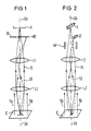
- the electron beam measuring device shown schematically in FIG. 1 is particularly suitable for carrying out the method according to the invention. It essentially consists of a beam generator with a cutting-edge cathode K, electron optics for focusing the primary electrons PE emitted by the cathode K and accelerated in the direction of an anode onto the sample IC to be examined, and a detector DT for detecting the secondary electrons triggered on the sample IC SE.
- an electron optic comprising the lenses L1 and L2 is provided, which images the primary electron source, which is linear due to the cathode geometry, onto the sample IC arranged immediately below the lens L2.
- An immersion lens serves as the objective lens L2, to the magnetic field of which is connected an electric field which brakes the primary electrons PE and accelerates the triggered secondary electrons SE against the primary beam direction.
- the strength of the electrical deceleration or acceleration field (symbolized by the arrows labeled U B ) built up in the space between the lens L2 and the sample IC is dimensioned such that the electron optics have an enlarged image of the secondary electron source, which is also linear due to the beam spot geometry Detector DT arranged in the beam path above the lens L1 is generated (only the beam path for the secondary electrons SE triggered at a point lying outside the optical axis OA is shown in FIG. 1).
- a line-shaped comes in particular as the detector DT Arrangement of semiconductor diodes into consideration, with each detector element HD being assigned a line element of the surface area illuminated by the primary beam. Since a large number of object points are scanned simultaneously with the primary beam and the triggered secondary electrons SE are detected in the detector elements HD assigned to the object points, the time for examining the sample IC is considerably reduced. A large-area scanning of the sample surface is achieved by deflecting the primary electron beam and / or by mechanically shifting the sample IC with respect to the optical axis OA.
- the secondary electrons SE accelerated in the electric field of the immersion lens OL can also be detected in a detector DT arranged outside the optical axis OA, a Vienna filter that does not influence the primary beam or an electrical or magnetic multipole element WF is used.
- the method according to the invention uses an electron probe with a beam cross section whose extent measured in a first direction is much larger than in a direction orthogonal to it (l x : l y > 10: 1).
- a line source which can for example also consist of a large number of individual sources arranged in a line, is used in the production of such an electron probe of the reducing electron-optical image. It is of course also possible to illuminate a slit diaphragm with a round or band-shaped electron beam and to scale the diaphragm opening down onto the sample IC. As FIG.
- the electron optics for illuminating the diaphragm SB having a rectangular passage opening BA comprise, for example, a round lens RL and a magnetic condenser lens KL, which are arranged directly below the electron beam generator Q.
- This preferably consists of a linear cathode K, in particular a LaB6 cutting Emitter with a flattened tip, a slit diaphragm W arranged in the region of the cathode tip and a double anode A, the electrodes of which are also designed as slit diaphragms (see FIG. 4 showing the radiation generator Q in plan view).
- the electron probe scanning the sample IC is composed of a plurality of partial beams if the diaphragm SB has a linear arrangement of square passage openings. It is advantageous here to feed each of the partial beams from its own source.
- electron sources are those from J. Vac. Sci. Technol. A5 (4), 1987, pages 1544 to 1548 known silicon cold cathodes, photocathodes (Appl. Phys. Lett. 51.2, 1987, pages 145 to 147), Lab6 single crystal cutting edge emitter (US-A-4 724 328) and the field emission cathodes described in SRI International Technical Note 2, November 1984.
- the invention is of course not limited to the exemplary embodiments described. This makes it easy to detect backscattered electrons in the detector instead of secondary electrons. Due to the beam spot geometry, these are also triggered in a linear area.
- Further lenses can be provided in the electron beam measuring device described in order to achieve the necessary reduction in size of the primary electron source or enlargement of the secondary particle source.
Landscapes
- Chemical & Material Sciences (AREA)
- Analytical Chemistry (AREA)
- Testing Or Measuring Of Semiconductors Or The Like (AREA)
- Analysing Materials By The Use Of Radiation (AREA)
- Tests Of Electronic Circuits (AREA)
Applications Claiming Priority (2)
| Application Number | Priority Date | Filing Date | Title |
|---|---|---|---|
| DE3902165 | 1989-01-25 | ||
| DE3902165 | 1989-01-25 |
Publications (3)
| Publication Number | Publication Date |
|---|---|
| EP0379865A2 true EP0379865A2 (fr) | 1990-08-01 |
| EP0379865A3 EP0379865A3 (fr) | 1991-06-05 |
| EP0379865B1 EP0379865B1 (fr) | 1994-12-28 |
Family
ID=6372776
Family Applications (1)
| Application Number | Title | Priority Date | Filing Date |
|---|---|---|---|
| EP90100170A Expired - Lifetime EP0379865B1 (fr) | 1989-01-25 | 1990-01-04 | Procédé d'examen d'un échantillon dans un appareil à faisceau corpusculaire |
Country Status (5)
| Country | Link |
|---|---|
| US (1) | US4954705A (fr) |
| EP (1) | EP0379865B1 (fr) |
| JP (1) | JP2831421B2 (fr) |
| CA (1) | CA1317035C (fr) |
| DE (1) | DE59008098D1 (fr) |
Cited By (4)
| Publication number | Priority date | Publication date | Assignee | Title |
|---|---|---|---|---|
| EP0518633A1 (fr) * | 1991-06-10 | 1992-12-16 | Fujitsu Limited | Appareil pour l'inspection de motif et appareil à faisceau électronique |
| EP0588572A1 (fr) * | 1992-09-17 | 1994-03-23 | Hitachi, Ltd. | Microscope électronique avec une caméra et son procédé d'utilisation |
| US5384463A (en) * | 1991-06-10 | 1995-01-24 | Fujisu Limited | Pattern inspection apparatus and electron beam apparatus |
| US5557105A (en) * | 1991-06-10 | 1996-09-17 | Fujitsu Limited | Pattern inspection apparatus and electron beam apparatus |
Families Citing this family (15)
| Publication number | Priority date | Publication date | Assignee | Title |
|---|---|---|---|---|
| EP0398335B1 (fr) * | 1989-05-17 | 1996-05-01 | KABUSHIKI KAISHA KOBE SEIKO SHO also known as Kobe Steel Ltd. | Dispositif pour focaliser un faisceau d'ions |
| JP3148353B2 (ja) * | 1991-05-30 | 2001-03-19 | ケーエルエー・インストルメンツ・コーポレーション | 電子ビーム検査方法とそのシステム |
| US5448399A (en) * | 1992-03-13 | 1995-09-05 | Park Scientific Instruments | Optical system for scanning microscope |
| WO1999009582A1 (fr) | 1997-08-19 | 1999-02-25 | Nikon Corporation | Dispositif et procede servant a observer un objet |
| US5973323A (en) * | 1997-11-05 | 1999-10-26 | Kla-Tencor Corporation | Apparatus and method for secondary electron emission microscope |
| JP3403036B2 (ja) * | 1997-11-14 | 2003-05-06 | 株式会社東芝 | 電子ビーム検査方法及びその装置 |
| JP4066078B2 (ja) * | 1999-05-27 | 2008-03-26 | 株式会社ニコン | 写像型電子顕微鏡 |
| WO2002001597A1 (fr) * | 2000-06-27 | 2002-01-03 | Ebara Corporation | Appareil d'inspection a faisceau de particules chargees et procede de fabrication d'un dispositif utilisant cet appareil d'inspection |
| JPWO2002037527A1 (ja) * | 2000-11-02 | 2004-03-11 | 株式会社荏原製作所 | 電子線装置及びその装置を用いたデバイス製造方法 |
| US6593152B2 (en) * | 2000-11-02 | 2003-07-15 | Ebara Corporation | Electron beam apparatus and method of manufacturing semiconductor device using the apparatus |
| JP4041742B2 (ja) * | 2001-05-01 | 2008-01-30 | 株式会社荏原製作所 | 電子線装置及び該電子線装置を用いたデバイス製造方法 |
| US6822246B2 (en) * | 2002-03-27 | 2004-11-23 | Kla-Tencor Technologies Corporation | Ribbon electron beam for inspection system |
| US6885000B1 (en) * | 2003-06-02 | 2005-04-26 | Kla-Tencor Technologies Corporation | Method and apparatus to correct for stage motion in E-beam inspection |
| US9257260B2 (en) * | 2013-04-27 | 2016-02-09 | Kla-Tencor Corporation | Method and system for adaptively scanning a sample during electron beam inspection |
| EP3716312A1 (fr) * | 2019-03-28 | 2020-09-30 | FEI Company | Dispositif à faisceau de particules chargées pour l'inspection d'un échantillon à l'aide d'une pluralité de mini-faisceaux de particules chargées |
Citations (5)
| Publication number | Priority date | Publication date | Assignee | Title |
|---|---|---|---|---|
| JPS60100349A (ja) * | 1983-11-07 | 1985-06-04 | Hitachi Ltd | 2次電子検出器 |
| GB2168839A (en) * | 1984-04-06 | 1986-06-25 | Hitachi Ltd | Secondary electron detector |
| EP0191440A1 (fr) * | 1985-02-12 | 1986-08-20 | Siemens Aktiengesellschaft | Appareil de lithographie pour la réalisation de microstructures |
| GB2183898A (en) * | 1985-11-05 | 1987-06-10 | Texas Instruments Ltd | Checking voltages in integrated circuit by means of an electron detector |
| US4769543A (en) * | 1986-03-07 | 1988-09-06 | Siemens Aktiengesellschaft | Spectrometer lens for particle beam apparatus |
Family Cites Families (4)
| Publication number | Priority date | Publication date | Assignee | Title |
|---|---|---|---|---|
| US1943109A (en) * | 1931-08-18 | 1934-01-09 | Gen Electric | Cathode ray sound recording |
| US3374386A (en) * | 1964-11-02 | 1968-03-19 | Field Emission Corp | Field emission cathode having tungsten miller indices 100 plane coated with zirconium, hafnium or magnesium on oxygen binder |
| US3875416A (en) * | 1970-06-30 | 1975-04-01 | Texas Instruments Inc | Methods and apparatus for the production of semiconductor devices by electron-beam patterning and devices produced thereby |
| DE8634545U1 (de) * | 1986-12-23 | 1987-05-21 | Siemens AG, 1000 Berlin und 8000 München | Korpuskularstrahlgerät zur fehlerarmen Abbildung linienförmiger Objekte |
-
1989
- 1989-09-13 CA CA000611162A patent/CA1317035C/fr not_active Expired - Fee Related
- 1989-10-02 US US07/416,996 patent/US4954705A/en not_active Expired - Lifetime
-
1990
- 1990-01-04 DE DE59008098T patent/DE59008098D1/de not_active Expired - Lifetime
- 1990-01-04 EP EP90100170A patent/EP0379865B1/fr not_active Expired - Lifetime
- 1990-01-22 JP JP2013438A patent/JP2831421B2/ja not_active Expired - Lifetime
Patent Citations (5)
| Publication number | Priority date | Publication date | Assignee | Title |
|---|---|---|---|---|
| JPS60100349A (ja) * | 1983-11-07 | 1985-06-04 | Hitachi Ltd | 2次電子検出器 |
| GB2168839A (en) * | 1984-04-06 | 1986-06-25 | Hitachi Ltd | Secondary electron detector |
| EP0191440A1 (fr) * | 1985-02-12 | 1986-08-20 | Siemens Aktiengesellschaft | Appareil de lithographie pour la réalisation de microstructures |
| GB2183898A (en) * | 1985-11-05 | 1987-06-10 | Texas Instruments Ltd | Checking voltages in integrated circuit by means of an electron detector |
| US4769543A (en) * | 1986-03-07 | 1988-09-06 | Siemens Aktiengesellschaft | Spectrometer lens for particle beam apparatus |
Non-Patent Citations (2)
| Title |
|---|
| PATENT ABSTRACTS OF JAPAN, Band 9, Nr. 251 (E-348)[1974], 8. Oktober 1985; & JP-A-60 100 349 (HITACHI) 04-06-1985 * |
| PROCEEDINGS OF THE EUROPEAN CONGRESS ON ELECTRON MICROSCOPY, Manchester, September 1972, Band 5, Institute of Physics, London, GB; V.G. GALSTYAN et al.: "The immersion objective as a secondary electron collector in the scanning electron microscope" * |
Cited By (6)
| Publication number | Priority date | Publication date | Assignee | Title |
|---|---|---|---|---|
| EP0518633A1 (fr) * | 1991-06-10 | 1992-12-16 | Fujitsu Limited | Appareil pour l'inspection de motif et appareil à faisceau électronique |
| US5384463A (en) * | 1991-06-10 | 1995-01-24 | Fujisu Limited | Pattern inspection apparatus and electron beam apparatus |
| US5430292A (en) * | 1991-06-10 | 1995-07-04 | Fujitsu Limited | Pattern inspection apparatus and electron beam apparatus |
| US5557105A (en) * | 1991-06-10 | 1996-09-17 | Fujitsu Limited | Pattern inspection apparatus and electron beam apparatus |
| EP0588572A1 (fr) * | 1992-09-17 | 1994-03-23 | Hitachi, Ltd. | Microscope électronique avec une caméra et son procédé d'utilisation |
| US5457317A (en) * | 1992-09-17 | 1995-10-10 | Hitachi, Ltd. | Electron microscope, a camera for such an electron microscope, and a method of operating such an electron microscope |
Also Published As
| Publication number | Publication date |
|---|---|
| EP0379865B1 (fr) | 1994-12-28 |
| DE59008098D1 (de) | 1995-02-09 |
| US4954705A (en) | 1990-09-04 |
| JPH02230649A (ja) | 1990-09-13 |
| EP0379865A3 (fr) | 1991-06-05 |
| JP2831421B2 (ja) | 1998-12-02 |
| CA1317035C (fr) | 1993-04-27 |
Similar Documents
| Publication | Publication Date | Title |
|---|---|---|
| EP0379865B1 (fr) | Procédé d'examen d'un échantillon dans un appareil à faisceau corpusculaire | |
| DE102006043895B4 (de) | Elektronenmikroskop zum Inspizieren und Bearbeiten eines Objekts mit miniaturisierten Strukturen | |
| DE60308482T2 (de) | Vorrichtung und Verfahren zur Untersuchung einer Probe eines Spezimen mittels eines Elektronenstrahls | |
| KR102179897B1 (ko) | 시료를 검사하기 위한 방법 및 하전 입자 다중-빔 디바이스 | |
| US7098455B2 (en) | Method of inspecting a circuit pattern and inspecting instrument | |
| EP0281743B1 (fr) | Objectif détecteur pour microscope à balayage | |
| US6465783B1 (en) | High-throughput specimen-inspection apparatus and methods utilizing multiple parallel charged particle beams and an array of multiple secondary-electron-detectors | |
| JP4920385B2 (ja) | 荷電粒子ビーム装置、走査型電子顕微鏡、及び試料観察方法 | |
| DE3532781A1 (de) | Anordnung zur detektion von sekundaer- und/oder rueckstreuelektronen in einem elektronenstrahlgeraet | |
| US7067807B2 (en) | Charged particle beam column and method of its operation | |
| DE112015002966T5 (de) | Vorbereitung des inspektionsortes | |
| DE112013000704T5 (de) | Rasterelektronenmikroskop | |
| DE3638682A1 (de) | Spektrometerobjektiv fuer korpuskularstrahlmesstechnik | |
| DE102012017950A1 (de) | Partikelstrahlmikroskop zur Erzeugung von Materialbestandteilen | |
| DE69133256T2 (de) | Rasterelekronenmikroskop und Bilderzeugungsverfahren | |
| JP2001074437A (ja) | 回路パターン検査装置及び回路パターン検査方法 | |
| DE112017007822B4 (de) | Rasterelektronenmikroskop | |
| DE102005014793B4 (de) | Verfahren und Inspektionssystem zur CD-Messung auf der Grundlage der Bestimmung von Flächenanteilen | |
| DE60127677T2 (de) | Elektronenstrahlvorrrichtung mit Mehrfachstrahl | |
| DE102021205394B4 (de) | Verfahren zum Betrieb eines Vielstrahlmikroskops mit an eine Inspektionsstelle angepassten Einstellungen | |
| US6670612B1 (en) | Undercut measurement using SEM | |
| DE102004025890B4 (de) | Substratinspektionsvorrichtung, Substratinspektionsverfahren und Verwendung des Verfahrens zum Herstellen einer Halbleitereinrichtung | |
| DE69918958T2 (de) | Rasterelektronenmikroskop mit einem ortssensitiven detektor | |
| DE102012215945A1 (de) | Teilchenstrahlgerät und Verfahren zum Betrieb eines Teilchenstrahlgeräts | |
| DE112019006527T5 (de) | Defektprüfvorrichtung und Defektprüfverfahren |
Legal Events
| Date | Code | Title | Description |
|---|---|---|---|
| PUAI | Public reference made under article 153(3) epc to a published international application that has entered the european phase |
Free format text: ORIGINAL CODE: 0009012 |
|
| AK | Designated contracting states |
Kind code of ref document: A2 Designated state(s): DE FR GB NL |
|
| 17P | Request for examination filed |
Effective date: 19901205 |
|
| PUAL | Search report despatched |
Free format text: ORIGINAL CODE: 0009013 |
|
| AK | Designated contracting states |
Kind code of ref document: A3 Designated state(s): DE FR GB NL |
|
| 17Q | First examination report despatched |
Effective date: 19940502 |
|
| GRAA | (expected) grant |
Free format text: ORIGINAL CODE: 0009210 |
|
| AK | Designated contracting states |
Kind code of ref document: B1 Designated state(s): DE FR GB NL |
|
| PG25 | Lapsed in a contracting state [announced via postgrant information from national office to epo] |
Ref country code: FR Effective date: 19941228 Ref country code: GB Effective date: 19941228 |
|
| REF | Corresponds to: |
Ref document number: 59008098 Country of ref document: DE Date of ref document: 19950209 |
|
| RAP2 | Party data changed (patent owner data changed or rights of a patent transferred) |
Owner name: ICT INTEGRATED CIRCUIT TESTING GESELLSCHAFT FUER H |
|
| EN | Fr: translation not filed | ||
| GBV | Gb: ep patent (uk) treated as always having been void in accordance with gb section 77(7)/1977 [no translation filed] |
Effective date: 19941228 |
|
| NLS | Nl: assignments of ep-patents |
Owner name: ICT INTEGRATED CIRCUIT TESTING GESELLSCHAFT FUER H |
|
| PLBE | No opposition filed within time limit |
Free format text: ORIGINAL CODE: 0009261 |
|
| STAA | Information on the status of an ep patent application or granted ep patent |
Free format text: STATUS: NO OPPOSITION FILED WITHIN TIME LIMIT |
|
| 26N | No opposition filed | ||
| PGFP | Annual fee paid to national office [announced via postgrant information from national office to epo] |
Ref country code: DE Payment date: 20090130 Year of fee payment: 20 Ref country code: NL Payment date: 20090113 Year of fee payment: 20 |
|
| NLV7 | Nl: ceased due to reaching the maximum lifetime of a patent |
Effective date: 20100104 |
|
| PG25 | Lapsed in a contracting state [announced via postgrant information from national office to epo] |
Ref country code: NL Free format text: LAPSE BECAUSE OF EXPIRATION OF PROTECTION Effective date: 20100104 |
|
| PG25 | Lapsed in a contracting state [announced via postgrant information from national office to epo] |
Ref country code: DE Free format text: LAPSE BECAUSE OF EXPIRATION OF PROTECTION Effective date: 20100104 |