EP0375919B1 - Calculating AC chip performance using the LSSD scan path - Google Patents
Calculating AC chip performance using the LSSD scan path Download PDFInfo
- Publication number
- EP0375919B1 EP0375919B1 EP89121376A EP89121376A EP0375919B1 EP 0375919 B1 EP0375919 B1 EP 0375919B1 EP 89121376 A EP89121376 A EP 89121376A EP 89121376 A EP89121376 A EP 89121376A EP 0375919 B1 EP0375919 B1 EP 0375919B1
- Authority
- EP
- European Patent Office
- Prior art keywords
- scan path
- lssd
- chip
- value
- control means
- Prior art date
- Legal status (The legal status is an assumption and is not a legal conclusion. Google has not performed a legal analysis and makes no representation as to the accuracy of the status listed.)
- Expired - Lifetime
Links
- 238000012360 testing method Methods 0.000 claims abstract description 55
- 238000005259 measurement Methods 0.000 claims abstract description 37
- 230000000644 propagated effect Effects 0.000 claims description 14
- 230000001902 propagating effect Effects 0.000 claims description 5
- 230000003213 activating effect Effects 0.000 claims description 2
- 238000010998 test method Methods 0.000 claims 1
- 238000013461 design Methods 0.000 abstract description 6
- 238000004519 manufacturing process Methods 0.000 abstract description 6
- 238000009434 installation Methods 0.000 abstract description 2
- 238000000034 method Methods 0.000 description 9
- 238000011010 flushing procedure Methods 0.000 description 5
- 230000002950 deficient Effects 0.000 description 3
- 230000006870 function Effects 0.000 description 2
- 230000036962 time dependent Effects 0.000 description 2
- 238000013459 approach Methods 0.000 description 1
- 230000009849 deactivation Effects 0.000 description 1
- 238000011161 development Methods 0.000 description 1
- 238000002955 isolation Methods 0.000 description 1
- 238000004806 packaging method and process Methods 0.000 description 1
Images
Classifications
-
- G—PHYSICS
- G01—MEASURING; TESTING
- G01R—MEASURING ELECTRIC VARIABLES; MEASURING MAGNETIC VARIABLES
- G01R31/00—Arrangements for testing electric properties; Arrangements for locating electric faults; Arrangements for electrical testing characterised by what is being tested not provided for elsewhere
- G01R31/28—Testing of electronic circuits, e.g. by signal tracer
- G01R31/317—Testing of digital circuits
- G01R31/3181—Functional testing
- G01R31/3185—Reconfiguring for testing, e.g. LSSD, partitioning
- G01R31/318533—Reconfiguring for testing, e.g. LSSD, partitioning using scanning techniques, e.g. LSSD, Boundary Scan, JTAG
- G01R31/318577—AC testing, e.g. current testing, burn-in
- G01R31/31858—Delay testing
Definitions
- the present invention relates to chip performance measurement, and in particular to the use of LSSD scan path circuit delay data in comparison with a predetermined value to evaluate overall AC chip performance.
- AC performance testing refers to dynamic time dependent testing, as opposed to DC stuck fault testing which is non-time dependent testing for purposes of error isolation.
- AC performance testing is performed during manufacture and test of circuitry using external test equipment.
- external test equipment used for AC performance testing is both expensive and inconvenient.
- LSSD scan path To characterize LSSD logic delay.
- flushing is defined as holding the clock inputs to an LSSD latch to an active level, thereby allowing a value placed on the input to the first latch in the scan path to scan through the scan path at the switching speed of the latches.
- This technique allows a single pass/fail result to be achieved for a test based on a given clock speed.
- this technique is not feasible for many situations, because the scan input or output is not accessible to probing by external test equipment for measurement due to packaging considerations.
- AC performance measurement is performed in a manufacturing or test environment and not in a field operational environment.
- a factor that limits the use of AC chip performance measurements in the field is that the measurements generally require precise and expensive external test equipment. Transporting such equipment around in the field is a highly undesirable practice. After circuits leave the manufacturing and test environment, AC defective circuits are difficult to detect in the field operational environment.
- AC chip performance testing often requires detailed knowledge of the underlying chip design in order to generate elaborate test data patterns to exercise the functional logic of each chip design to obtain a measurement. Test data patterns are expensive to generate because they must be individually created for each particular circuit design. In addition, AC performance testing is done on a pass/fail basis for a given clock speed.
- a system using the LSSD circuitry on a chip to obtain AC performance measurements by propagating a signal through the LSSD scan path which is usually the longest path on the chip is provided.
- Logic means control propagation of the signal through the LSSD scan path for a predetermined period of time.
- the distance through the LSSD scan path which the signal has been propagated is a function of the AC performance characteristics of the chip.
- the LSSD scan path is analyzed to determine how far the signal has propagated through the scan path.
- a value indicative of the distance the signal was propagated through the scan path is used as AC timing measurement data.
- Comparison means compares the AC timing measurement data with predetermined AC classification data which is stored in the system to determine the overall classification of the chip as one of a plurality of possible chip performance classes.
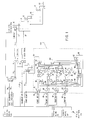
- Fig.1 is a schematic representation of the calibration logic used in the invention for testing AC performance.
- the invention disclosed herein makes use of the LSSD scan path, which is commonly used in prior art testing schemes for DC stuck fault testing, to generate AC chip performance measurements.
- the very LSSD latches whose AC performance is to be measured, form a part of the apparatus used for the measurement.
- the measurement begins by placing the LSSD chip in scan mode, which arranges the latches on the chip into a scan path having a serial configuration.
- the latches are controlled by three signals. Two of the signals are clocks, both of which must be at an active level to propagate a signal.
- the third signal is the value which is to be propagated.
- the scan path is first flushed by holding both clocks in an active state and placing a uniform value on the third line.
- the clocks Since the clocks are held active, the signal will be flushed through the scan path at the switching speed of the circuitry.
- the clock signals are ideally held active for a period which is long enough to flush the entire scan path. After the scan path is flushed, one of the clock lines is placed in an inactive state. It does not matter which clock line is deactivated to accomplish the purpose of the invention since the LSSD scan path requires both clock lines to be up in order to propagate a signal through the scan path, the deactivation of either clock line terminates the flush operation.
- the measurement operation begins.
- the uniform value on the third line is inverted.
- a predetermined time value is placed in clock control means which control the amount of time that will be allocated for the propagation of the third signal value.
- the predetermined time value can be generated in any number of ways, including software programming or hardware implementation.
- the preferred embodiment uses clock control means which are treated herein as part of the logic control means.
- the clock control means are a binary decrementing counter 130 which is well known in the art.
- the deactivated clock signal is activated and the value on the third signal line begins to flush through the scan path.
- the clock control means halts the propagation of the uniform value through the scan path.
- the distance the value has propagated through the scan path which is a function of AC chip performance, can be determined. After the distance the propagated value has traveled through the scan path is determined, it is compared to a table of predetermined values that represent categories of AC chip performance for that particular chip design. The AC chip performance is categorized according to the results of the comparison.
- the logic control means 146, the comparison means 144, and the storage means 142 are all shown as part of the service processor 140. This is optional as each of the foregoing components could be located elsewhere in the system in the form of hardware embodiments.
- the comparison means 144, and the portions of the logic control means 146 could be implemented in software.
- portions of the logic control means 146, including the clock control means which is a binary decrementing counter 130, and some additional control latches 2, 4, 6, are shown separately from the remainder of the logic control means 146 in figure 1.
- the signals that drive the AC performance measurement operation, including the predetermined time value are generated by the logic control means 146.
- AC performance testing using LSSD scan path measurement is accomplished by first turning off the system clock. Once the clock has been turned off, the service processor 140 then initializes scan mode which involves configuring the LSSD latches in the LSSD circuit into a serial chain called the LSSD scan path. Scan mode is well known in the art of LSSD circuitry.
- the logic control means produce AC timing measurement data by controlling the execution of the AC performance measurement.
- the logic control means 146 begins AC measurement by flushing a value on Scan In line 62 through the LSSD scan path 10, 12, 14 for the purpose of setting all latches to a uniform value.
- a flushing operation does not rely on clock pulses, but instead propagates a signal through the LSSD scan path 10, 12, 14 at a rate determined solely by circuit delay.
- the flush operation is controlled by the A clock signal on line 60 and the B clock signal on line 70, which are controlled by the logic control means 146.
- the A clock signal on line 60 and the B clock signal on line 70 are controlled by the logic control means 146 including latches 2, 4, 6, and counter 130.
- the value to be flushed is generated by the logic control means 146 and is placed on the Scan In line 62.
- the particular value selected for placement on the Scan In line 62 is irrelevant. It is only important that the value does not change during the flush operation, and that the value flushed through the LSSD scan path 10, 12, 14 in the measurement step is an different from the value used in the flush step so that its propagation termination point can be found.
- a binary decrementing counter 130 is provided to create a delay which determines the duration of the flush operation.
- a predetermined time value is selected by the logic control means 146 and placed on lines 78, 80, 82, 84 which allows enough time to flush the entire LSSD scan path 10, 12, 14.
- the B clock is turned off when counter 130 decrements to one, thereby stopping propagation in the LSSD scan path 10, 12, 14. Then the value on the Scan In line 62 is changed by the logic control means 146. The value is changed from the previous value propagated through the LSSD scan path 10, 12, 14 so that when it is propagated partially through the LSSD scan path 10, 12, 14, its termination point can be detected.
- a B clock pulse of predetermined width is generated which propagates the changed value of the Scan In signal on line 62 through the LSSD scan path 10, 12, 14. The pulse width is selected such that the Scan In value on line 62 does not propagate through the entire LSSD scan path 10, 12, 14.
- the pulse width is selected by the logic control means 146 according to the number of LSSD latches on the chip. The shorter the scan path on the chip, the narrower the pulse width. Correspondingly, the longer the scan path, the wider the pulse width. While a narrow pulse width selected for a short scan path would work on longer scan paths, selecting wider pulse widths allows more accurate measurements to be made.
- Use of the counter 130 allows the logic control means 146 to program the pulse width for the LSSD scan path 10, 12, 14. In turn, this allows a single counter 130 to be used for multiple LSSD circuits having a wide range of possible scan path lengths. The selection of the appropriate pulse width can be implemented in a number of ways, including hardware implementation or through software programming control.
- the new value on the Scan In signal on line 62 begins to flush though the LSSD scan path 10, 12, 14.
- the B clock pulse on line 70 stops the flush operation.
- the scan in data has propagated partially through the LSSD scan path 10, 12, 14.
- Known LSSD techniques can then be used to determine how far the Scan In signal has propagated by serially shifting the data in the scan path. The value which defines the distance that the Scan In signal on line 62 had propagated through the LSSD scan path 10, 12, 14 is used as the AC timing measurement data.
- Comparison means 144 are used to compare the AC timing measurement data with the predetermined AC performance classification data held in storage means 142 which represents a plurality of possible AC chip performance categories.
- the AC performance classification data only needs to be created once when the chip is designed and does not have to be recreated thereafter. Typically, as many as ten or more categories might be used. However, for purposes of illustration, it will be assumed that three categories, representing fast, nominal, and slow chips are used.
- the logic control means 146 flushes the LSSD scan path 10, 12, 14 under control of the three control lines, 60, 62, 70.
- the placement of an LSSD circuit in scan mode is well known in the art.
- the logical state which is to be flushed through the LSSD scan path is placed on Scan In line 62.
- the control lines 60, 70 are placed in an active state as follows: the logic control means 146 activate the Start Calibrate signal 54 and the Calibrate Op signal 128, they in turn activate gate 4 which which activates the A clock signal on line 60. Because the Reset Calibrate signal on line 56 is not active at this time, the Start Calibrate signal turns on latch 2 which provides the other input to gate 4.
- the A clock control signal 60 is controlled by activating AND gate 4.
- the B clock is activated when the logic control means 146 activates the Start Count signal on line 74 and places a predetermined time value on lines 78, 80, 82, 84 which starts the counter 130.
- Latch 8 which is initially in the inactive state, is turned on by the Start Count signal on line 74, which is activated for one cycle by the service processor 140.
- the Start Count signal also gates count bits 0-3 on lines 78, 80, 82, 84 which are initialized by the logic control means 146 to contain a value indicating the duration of time to flush the LSSD scan path 10, 12, 14.
- the counter gate 48 and the Start Count signal on line 74 activate latch 8 which was initially in the inactive state, which in combination with the active Calibrate Op signal on line 128 activates gate 6 turning on the B clock on line 70.
- the three control lines 60, 62, 70 are held in the selected states for a duration long enough to allow propagation of the Scan In signal 62 through the LSSD scan path 10, 12, 14.
- the predetermined time value selected by the logic control means 146 is placed in gates 16, 18, 20, 22 of the counter 130 and decremented under control of clock pulses on lines 112, 114, 116, 118, 120, 122, 124, 126. How to generate the clock pulses on lines 112, 114, 116, 118, 120, 122, 124, 126 is well known and can be provided by the system oscillator among other sources.
- the counter itself is a conventional 4-bit decrementing binary counter which is known in the art. When the value in the counter is equal to one, the circuit 48 is activated, which resets latch 8. Latch 8, in turn, resets the B clock signal on line 70 which terminates propagation through the LSSD scan path 10, 12, 14. Then, when the counter 130 decrements to zero, circuit 52 disables the counter 130 and freezes the value at zero thus resetting the signal on control line 76 to allow the next count operation to be executed.
- the LSSD scan path 10, 12, 14 has been flushed and AC performance scan path measurement is about to begin.
- the A clock signal on line 60 is still active at this time and the B clock signal on line 70 is inactive.
- the Scan In signal on line 62 is set to the opposite value by the logic control means 146.
- the Calibrate Op signal on line 128 is still active at this time.
- the predetermined time value which indicates the duration of the scan will be selected by the logic control means 146 and placed on lines 78, 80, 82, 84.
- AC measurement is begun by the logic control means 146 when the Start Count signal on line 74 is activated for one cycle. Simultaneously, the Start Count signal on line 74 activates latch 8 which enables gate 6.
- Gate 6 activates the B clock signal on line 70 which begins a flush operation through the LSSD scan path 10, 12, 14.
- the LSSD scan path 10, 12, 14 continues the flush operation until it is reset by the counter 130 which resets latch 8 in the same manner as was done when the LSSD scan path 10, 12, 14 was initialized.
- the Scan In signal on line 62 stops propagating through the LSSD scan path 10, 12, 14.
- the logic control means 146 activates the Reset Calibrate signal on line 56 which turns off the A clock on line 60.
- the AC performance classification data used to compare with the AC timing measurement data to categorize the AC chip performance is in storage means 142 within the service processor 140.
- it can be stored at any conveniently accessible place, which can be in the service processor 140, a system storage device, or even at a remote location.
- the comparison means 144 do not have to be located in the service processor. It can also be located wherever it is convenient. For example, a remote processor could be used by service personnel to evaluate the AC chip performance at a distance, thereby providing highly skilled technical personnel access to the system without requiring their presence on site.
- the invention has many advantages including the ability to categorize AC chip performance data in a single pass, the ability to execute without external test equipment, and the ability to measure AC chip performance in field operational environments as well as in manufacturing and test environments.
- the storage means 142, comparison means 144, and logic control means 146, shown as part of the service processor 140 could be implemented separate from the service processor 140 in a variety of ways, such as on disk, bubble memory, or even at a remote location. Additionally, other features such as the comparison can be made locally or remotely. Details of the circuit can also vary. For example, the A clock can be used to control the pulse width instead of the B clock. Also, the Scan In control line 62 can be activated at any point during the flush operation. Also, the programmable clock control logic could be implemented in software. Accordingly, the invention herein disclosed is to be limited only as specified in the following claims.
Landscapes
- Engineering & Computer Science (AREA)
- Power Engineering (AREA)
- General Engineering & Computer Science (AREA)
- Physics & Mathematics (AREA)
- General Physics & Mathematics (AREA)
- Tests Of Electronic Circuits (AREA)
- Testing Or Measuring Of Semiconductors Or The Like (AREA)
- Test And Diagnosis Of Digital Computers (AREA)
Abstract
Description
- The present invention relates to chip performance measurement, and in particular to the use of LSSD scan path circuit delay data in comparison with a predetermined value to evaluate overall AC chip performance.
- The continuing increase in complexity and speed of electronic circuitry has posed numerous problems in measurement or testing of circuits to ensure that they meet minimum performance criteria. In particular, the development and use of integrated circuits of ever increasing size and complexity has posed numerous problems in the area of AC performance testing in a field operational environment. The difficulties involved in AC performance testing present additional problems in an field operational environment due to the complexity of tests, the expensive and inconvenient nature of the test equipment, and the possibility of not detecting AC defective circuits with known techniques. For purposes of this patent application, AC performance testing refers to dynamic time dependent testing, as opposed to DC stuck fault testing which is non-time dependent testing for purposes of error isolation.
- Typically, AC performance testing is performed during manufacture and test of circuitry using external test equipment. One reason why testing is not done when the circuitry is installed in a field operational environment is that the external test equipment used for AC performance testing is both expensive and inconvenient.
- It is known to use the LSSD scan path to characterize LSSD logic delay. In that method, a measurement is used wherein the clocks are turned on, and a signal is flushed entirely through the scan path. For purposes of this disclosure, flushing is defined as holding the clock inputs to an LSSD latch to an active level, thereby allowing a value placed on the input to the first latch in the scan path to scan through the scan path at the switching speed of the latches. This technique allows a single pass/fail result to be achieved for a test based on a given clock speed. However, this technique is not feasible for many situations, because the scan input or output is not accessible to probing by external test equipment for measurement due to packaging considerations.
- It is also known to do performance testing through the use of complicated test patterns which exercise the functional logic unique to each chip. When using complicated test patterns, the path lengths are typically short compared to the LSSD scan path. This results in measurements which require very precise test equipment for accuracy which causes high cost to obtain the measurement data. Further, such prior attempts at testing have only been able to test on a pass/fail basis for a given clock speed.
- Another prior art approach at pass/fail testing is to use clock shifting to allow testing with less expensive testers. However, the same problems of inability to detect marginal circuits due to the pass/fail nature of the test, and the expense and inconvenience of using external testers in the field apply to this method, just as they did to the methods discussed previously.
- Document IBM TDB Vol.29, No.3, August 1986, pages 1234-1236 discloses a method for testing AC performance levels in LSSD integrated circuit chips comprising the steps of: a) placing an LSSD integrated circuit having a plurality of latches in scan mode, wherein each of said latches is placed serially in a scan path and each latch in the scan path is set to a first uniform value; b) propagating a second uniform value through said scan path for a predetermined period of time, and measuring the number of latches in said scan path through which said second uniform signal propagated to obtain a measured value; c) comparing said measured value with predetermined AC performance classification data. Said document, however, suffers from the drawback that it firstly needs an external tester as in-system test circuitry is not provided and secondly that a number of measuring cycles are necessary to arrive at trustworthy and reliable test results.
- In summary of the problems associated with the prior art, typically, AC performance measurement is performed in a manufacturing or test environment and not in a field operational environment. A factor that limits the use of AC chip performance measurements in the field is that the measurements generally require precise and expensive external test equipment. Transporting such equipment around in the field is a highly undesirable practice. After circuits leave the manufacturing and test environment, AC defective circuits are difficult to detect in the field operational environment.
- Further, AC chip performance testing often requires detailed knowledge of the underlying chip design in order to generate elaborate test data patterns to exercise the functional logic of each chip design to obtain a measurement. Test data patterns are expensive to generate because they must be individually created for each particular circuit design. In addition, AC performance testing is done on a pass/fail basis for a given clock speed.
- It is an object of this invention to improve testing and calibration of AC chip performance.
- It is another object of this invention to categorize AC chip performance with a single scan of the LSSD scan path.
- It is a further object of this invention to test AC chip performance without requiring test circuitry external to the system.
- It is yet another object of this invention to test chips without generating detailed test pattern data for each chip design.
- It is yet a further object of this invention to detect AC defective chips after installation of the chip in an operational environment which were not detected in a manufacturing and testing environment.
- These an other objects are accomplished by
apparatus claim 1 and method claim 5. A system using the LSSD circuitry on a chip to obtain AC performance measurements by propagating a signal through the LSSD scan path which is usually the longest path on the chip is provided. Logic means control propagation of the signal through the LSSD scan path for a predetermined period of time. The distance through the LSSD scan path which the signal has been propagated is a function of the AC performance characteristics of the chip. After propagation is halted by the logic means, the LSSD scan path is analyzed to determine how far the signal has propagated through the scan path. A value indicative of the distance the signal was propagated through the scan path is used as AC timing measurement data. Comparison means then compares the AC timing measurement data with predetermined AC classification data which is stored in the system to determine the overall classification of the chip as one of a plurality of possible chip performance classes. - Fig.1 is a schematic representation of the calibration logic used in the invention for testing AC performance.
- Prior to discussing the detailed description of the invention, the following is a broad overview of the invention.
- The invention disclosed herein, makes use of the LSSD scan path, which is commonly used in prior art testing schemes for DC stuck fault testing, to generate AC chip performance measurements. Further, the very LSSD latches, whose AC performance is to be measured, form a part of the apparatus used for the measurement. The measurement begins by placing the LSSD chip in scan mode, which arranges the latches on the chip into a scan path having a serial configuration. In scan mode, the latches are controlled by three signals. Two of the signals are clocks, both of which must be at an active level to propagate a signal. The third signal is the value which is to be propagated. The scan path is first flushed by holding both clocks in an active state and placing a uniform value on the third line. Since the clocks are held active, the signal will be flushed through the scan path at the switching speed of the circuitry. The clock signals are ideally held active for a period which is long enough to flush the entire scan path. After the scan path is flushed, one of the clock lines is placed in an inactive state. It does not matter which clock line is deactivated to accomplish the purpose of the invention since the LSSD scan path requires both clock lines to be up in order to propagate a signal through the scan path, the deactivation of either clock line terminates the flush operation.
- After the flush operation is complete, the measurement operation begins. The uniform value on the third line is inverted. Then, a predetermined time value is placed in clock control means which control the amount of time that will be allocated for the propagation of the third signal value. The predetermined time value can be generated in any number of ways, including software programming or hardware implementation. The preferred embodiment uses clock control means which are treated herein as part of the logic control means. The clock control means are a binary decrementing
counter 130 which is well known in the art. The deactivated clock signal is activated and the value on the third signal line begins to flush through the scan path. When the time limit defined by the predetermined time value is reached, the clock control means halts the propagation of the uniform value through the scan path. At this point, the distance the value has propagated through the scan path, which is a function of AC chip performance, can be determined. After the distance the propagated value has traveled through the scan path is determined, it is compared to a table of predetermined values that represent categories of AC chip performance for that particular chip design. The AC chip performance is categorized according to the results of the comparison. - Now, with regard to the detailed preferred embodiment, as shown in figure 1, the logic control means 146, the comparison means 144, and the storage means 142 are all shown as part of the
service processor 140. This is optional as each of the foregoing components could be located elsewhere in the system in the form of hardware embodiments. In addition, the comparison means 144, and the portions of the logic control means 146 could be implemented in software. For ease of illustration, portions of the logic control means 146, including the clock control means which is abinary decrementing counter 130, and some additional control latches 2, 4, 6, are shown separately from the remainder of the logic control means 146 in figure 1. The signals that drive the AC performance measurement operation, including the predetermined time value are generated by the logic control means 146. - To explain the operation, AC performance testing using LSSD scan path measurement is accomplished by first turning off the system clock. Once the clock has been turned off, the
service processor 140 then initializes scan mode which involves configuring the LSSD latches in the LSSD circuit into a serial chain called the LSSD scan path. Scan mode is well known in the art of LSSD circuitry. - The logic control means produce AC timing measurement data by controlling the execution of the AC performance measurement. The logic control means 146 begins AC measurement by flushing a value on Scan In line 62 through the
LSSD scan path LSSD scan path - The flush operation is controlled by the A clock signal on
line 60 and the B clock signal online 70, which are controlled by the logic control means 146. The A clock signal online 60 and the B clock signal online 70 are controlled by the logic control means 146 includinglatches counter 130. The value to be flushed is generated by the logic control means 146 and is placed on the Scan In line 62. The particular value selected for placement on the Scan In line 62 is irrelevant. It is only important that the value does not change during the flush operation, and that the value flushed through theLSSD scan path - After the flushing operation has begun a
binary decrementing counter 130 is provided to create a delay which determines the duration of the flush operation. A predetermined time value is selected by the logic control means 146 and placed onlines LSSD scan path - After the flush operation has been completed, the B clock is turned off when counter 130 decrements to one, thereby stopping propagation in the
LSSD scan path LSSD scan path LSSD scan path LSSD scan path LSSD scan path - The pulse width is selected by the logic control means 146 according to the number of LSSD latches on the chip. The shorter the scan path on the chip, the narrower the pulse width. Correspondingly, the longer the scan path, the wider the pulse width. While a narrow pulse width selected for a short scan path would work on longer scan paths, selecting wider pulse widths allows more accurate measurements to be made. Use of the
counter 130 allows the logic control means 146 to program the pulse width for theLSSD scan path single counter 130 to be used for multiple LSSD circuits having a wide range of possible scan path lengths. The selection of the appropriate pulse width can be implemented in a number of ways, including hardware implementation or through software programming control. - When the B clock pulse is activated by the logic control means 146, the new value on the Scan In signal on line 62, which was set after the flushing operation was complete, begins to flush though the
LSSD scan path line 70 is terminated, it stops the flush operation. At that time, the scan in data has propagated partially through theLSSD scan path LSSD scan path - Comparison means 144 are used to compare the AC timing measurement data with the predetermined AC performance classification data held in storage means 142 which represents a plurality of possible AC chip performance categories. The AC performance classification data only needs to be created once when the chip is designed and does not have to be recreated thereafter. Typically, as many as ten or more categories might be used. However, for purposes of illustration, it will be assumed that three categories, representing fast, nominal, and slow chips are used.
- Referring to figure 1, once the
LSSD scan path LSSD scan path control lines signal 54 and the Calibrate Op signal 128, they in turn activate gate 4 which which activates the A clock signal online 60. Because the Reset Calibrate signal online 56 is not active at this time, the Start Calibrate signal turns onlatch 2 which provides the other input to gate 4. The Aclock control signal 60 is controlled by activating AND gate 4. - The B clock is activated when the logic control means 146 activates the Start Count signal on
line 74 and places a predetermined time value onlines counter 130.Latch 8, which is initially in the inactive state, is turned on by the Start Count signal online 74, which is activated for one cycle by theservice processor 140. The Start Count signal also gates count bits 0-3 onlines LSSD scan path counter gate 48 and the Start Count signal online 74 activatelatch 8 which was initially in the inactive state, which in combination with the active Calibrate Op signal on line 128 activatesgate 6 turning on the B clock online 70. The threecontrol lines LSSD scan path - The predetermined time value selected by the logic control means 146 is placed in
gates counter 130 and decremented under control of clock pulses onlines lines circuit 48 is activated, which resetslatch 8.Latch 8, in turn, resets the B clock signal online 70 which terminates propagation through theLSSD scan path counter 130 decrements to zero,circuit 52 disables thecounter 130 and freezes the value at zero thus resetting the signal on control line 76 to allow the next count operation to be executed. - At this point, the
LSSD scan path line 60 is still active at this time and the B clock signal online 70 is inactive. Next, the Scan In signal on line 62 is set to the opposite value by the logic control means 146. The Calibrate Op signal on line 128 is still active at this time. The predetermined time value which indicates the duration of the scan will be selected by the logic control means 146 and placed onlines line 74 is activated for one cycle. Simultaneously, the Start Count signal online 74 activates latch 8 which enablesgate 6.Gate 6 activates the B clock signal online 70 which begins a flush operation through theLSSD scan path LSSD scan path counter 130 which resetslatch 8 in the same manner as was done when theLSSD scan path line 70 is deactivated by thecounter 130, the Scan In signal on line 62 stops propagating through theLSSD scan path line 56 which turns off the A clock online 60. - For the purpose of describing the preferred embodiment, the AC performance classification data used to compare with the AC timing measurement data to categorize the AC chip performance is in storage means 142 within the
service processor 140. However, it can be stored at any conveniently accessible place, which can be in theservice processor 140, a system storage device, or even at a remote location. Further, the comparison means 144 do not have to be located in the service processor. It can also be located wherever it is convenient. For example, a remote processor could be used by service personnel to evaluate the AC chip performance at a distance, thereby providing highly skilled technical personnel access to the system without requiring their presence on site. - The invention has many advantages including the ability to categorize AC chip performance data in a single pass, the ability to execute without external test equipment, and the ability to measure AC chip performance in field operational environments as well as in manufacturing and test environments.
- The storage means 142, comparison means 144, and logic control means 146, shown as part of the
service processor 140 could be implemented separate from theservice processor 140 in a variety of ways, such as on disk, bubble memory, or even at a remote location. Additionally, other features such as the comparison can be made locally or remotely. Details of the circuit can also vary. For example, the A clock can be used to control the pulse width instead of the B clock. Also, the Scan In control line 62 can be activated at any point during the flush operation. Also, the programmable clock control logic could be implemented in software. Accordingly, the invention herein disclosed is to be limited only as specified in the following claims.
Claims (5)
- Apparatus for testing AC performance levels in LSSD integrated circuit chips, said apparatus integrated into a system having LSSD integrated circuit chips under test, said apparatus comprising:
an LSSD integrated circuit to be tested and having an LSSD scan path (62) and clock lines (60, 70);
logic control means (146) including scan path flush means for initializing each latch (10, 12, 14) in said LSSD scan path to a first uniform value;
time measuring means (130) for measuring a predetermined time period provided by said logic control means (146);
clock control means (2,4,6,8), coupled to said logic control means (146) and measuring means (130), for activating and deactivating said clock lines in conformance with said predetermined time period to generate AC timing measurement data within said LSSD scan path, said AC timing measurement data defining a propagation distance to which a scanning signal has propagated through said LSSD scan path, said clock control means (2,4,6,8) producing a clock pulse (A or B) of predetermined width for controlling the amount of time allowed for propagating a second uniform value, different to said first uniform value, through said LSSD scan path, the distance said second uniform value has propagated through the scan path defining said propagation distance;
storage means (142) for storing AC chip performance classification data; and
comparison means (144) for comparing said AC timing measurement data with said AC performance classification data, wherein said integrated circuit is classified according to overall AC circuit performance. - Apparatus as in claim 1, wherein said logic control means (146) further includes means for programming the width of said clock signals.
- Apparatus as in claims 1 or 2, characterized in that said means for measuring a predetermined time period comprises a counter (130) which is initially set by said logic control means (146) to a predetermined value which is then decremented to a final value (0 or 1) thus providing said predetermined time period.
- Apparatus as in claim 3, characterized in that said predetermined values represent the LSSD paths lengths inherent in said LSSD integrated circuit chip under test and which are stored in said integrated apparatus.
- Method of testing AC performance levels in LSSD integrated circuit chips using the apparatus of claim 1, the latches of which are first placed serially in a scan path flush mode;
placing thereafter said scan path in scan mode in which each latch is set to a first uniform value;
propagating a second uniform value different to said first uniform value through said scan path for a predetermined period of time which is produced by applying to each latch of said scan path a clock pulse (A or B) of predetermined width where said predetermined pulse width is equal in time to said predetermined period of time ;
determining the number of latches in said scan path which were penetrated by said second uniform values to obtain a measured value, eg., an AC timing measurement data defining a propagation distance;
comparing said measured value with predetermined AC performance classification data; and
categorizing the AC chip performance of the LSSD circuit based on the comparison of the measured value.
Applications Claiming Priority (2)
| Application Number | Priority Date | Filing Date | Title |
|---|---|---|---|
| US07/291,919 US5039939A (en) | 1988-12-29 | 1988-12-29 | Calculating AC chip performance using the LSSD scan path |
| US291919 | 1988-12-29 |
Publications (3)
| Publication Number | Publication Date |
|---|---|
| EP0375919A2 EP0375919A2 (en) | 1990-07-04 |
| EP0375919A3 EP0375919A3 (en) | 1991-08-21 |
| EP0375919B1 true EP0375919B1 (en) | 1995-08-30 |
Family
ID=23122434
Family Applications (1)
| Application Number | Title | Priority Date | Filing Date |
|---|---|---|---|
| EP89121376A Expired - Lifetime EP0375919B1 (en) | 1988-12-29 | 1989-11-18 | Calculating AC chip performance using the LSSD scan path |
Country Status (4)
| Country | Link |
|---|---|
| US (1) | US5039939A (en) |
| EP (1) | EP0375919B1 (en) |
| JP (1) | JPH0812227B2 (en) |
| DE (1) | DE68924053T2 (en) |
Families Citing this family (7)
| Publication number | Priority date | Publication date | Assignee | Title |
|---|---|---|---|---|
| JPH05307619A (en) * | 1991-05-16 | 1993-11-19 | Nec Corp | Method for measuring ac characteristic of microprocessor |
| US5796751A (en) * | 1996-07-22 | 1998-08-18 | International Business Machines Corporation | Technique for sorting high frequency integrated circuits |
| US6219813B1 (en) | 1998-06-29 | 2001-04-17 | International Business Machines Corporation | Programmable timing circuit for testing the cycle time of functional circuits on an integrated circuit chip |
| EP0992809A1 (en) * | 1998-09-28 | 2000-04-12 | Siemens Aktiengesellschaft | Circuit with deactivatable scan path |
| US6452435B1 (en) | 1999-11-08 | 2002-09-17 | International Business Machines Corporation | Method and apparatus for scanning and clocking chips with a high-speed free running clock in a manufacturing test environment |
| JP2002202348A (en) * | 2000-12-28 | 2002-07-19 | Nec Microsystems Ltd | Test circuit for logic ic and method therefor |
| US7539893B1 (en) | 2005-09-16 | 2009-05-26 | Pmc-Sierra, Inc. | Systems and methods for speed binning of integrated circuits |
Family Cites Families (13)
| Publication number | Priority date | Publication date | Assignee | Title |
|---|---|---|---|---|
| US3784907A (en) * | 1972-10-16 | 1974-01-08 | Ibm | Method of propagation delay testing a functional logic system |
| US4063080A (en) * | 1976-06-30 | 1977-12-13 | International Business Machines Corporation | Method of propagation delay testing a level sensitive array logic system |
| JPS5499540A (en) * | 1978-01-23 | 1979-08-06 | Omron Tateisi Electronics Co | Malfunction detecting device for electronic circuit |
| US4293919A (en) * | 1979-08-13 | 1981-10-06 | International Business Machines Corporation | Level sensitive scan design (LSSD) system |
| DE3029883A1 (en) * | 1980-08-07 | 1982-03-11 | Ibm Deutschland Gmbh, 7000 Stuttgart | SLIDE REGISTER FOR TEST AND TEST PURPOSES |
| US4450560A (en) * | 1981-10-09 | 1984-05-22 | Teradyne, Inc. | Tester for LSI devices and memory devices |
| US4477902A (en) * | 1982-06-18 | 1984-10-16 | Ibm Corporation | Testing method for assuring AC performance of high performance random logic designs using low speed tester |
| US4513418A (en) * | 1982-11-08 | 1985-04-23 | International Business Machines Corporation | Simultaneous self-testing system |
| US4564943A (en) * | 1983-07-05 | 1986-01-14 | International Business Machines | System path stressing |
| DE3325247A1 (en) * | 1983-07-13 | 1985-01-24 | ANT Nachrichtentechnik GmbH, 7150 Backnang | CIRCUIT ARRANGEMENT FOR TESTING A DIGITAL CIRCUIT |
| US4602210A (en) * | 1984-12-28 | 1986-07-22 | General Electric Company | Multiplexed-access scan testable integrated circuit |
| JPS63101783A (en) * | 1986-10-20 | 1988-05-06 | Matsushita Electronics Corp | Semiconductive integrated circuit device |
| JPS63235874A (en) * | 1987-03-24 | 1988-09-30 | Mitsubishi Electric Corp | Semiconductor integrated circuit |
-
1988
- 1988-12-29 US US07/291,919 patent/US5039939A/en not_active Expired - Fee Related
-
1989
- 1989-11-18 DE DE68924053T patent/DE68924053T2/en not_active Expired - Fee Related
- 1989-11-18 EP EP89121376A patent/EP0375919B1/en not_active Expired - Lifetime
- 1989-12-20 JP JP1328622A patent/JPH0812227B2/en not_active Expired - Lifetime
Also Published As
| Publication number | Publication date |
|---|---|
| EP0375919A3 (en) | 1991-08-21 |
| JPH0812227B2 (en) | 1996-02-07 |
| EP0375919A2 (en) | 1990-07-04 |
| US5039939A (en) | 1991-08-13 |
| JPH02226077A (en) | 1990-09-07 |
| DE68924053T2 (en) | 1996-05-02 |
| DE68924053D1 (en) | 1995-10-05 |
Similar Documents
| Publication | Publication Date | Title |
|---|---|---|
| EP0161639B1 (en) | Self contained array timing | |
| US5923676A (en) | Bist architecture for measurement of integrated circuit delays | |
| US4878209A (en) | Macro performance test | |
| US5206861A (en) | System timing analysis by self-timing logic and clock paths | |
| US7944229B2 (en) | Method and apparatus for calibrating internal pulses in an integrated circuit | |
| US3621387A (en) | Computer-controlled tester for integrated circuit devices | |
| KR960005606B1 (en) | Built-in test circuit and speed test method to provide simple and accurate AC (AC) test of digital microcircuits using low bandwidth test equipment and probe stations | |
| US8543966B2 (en) | Test path selection and test program generation for performance testing integrated circuit chips | |
| EP0366553B1 (en) | Test device and method for testing electronic device and semiconductor device having the test device | |
| US20030169070A1 (en) | Method and apparatus for built-in self-test of logic circuits with multiple clock domains | |
| JPS63175780A (en) | Logic integrated circuit | |
| US20080071489A1 (en) | Integrated circuit for measuring set-up and hold times for a latch element | |
| EP0054111B1 (en) | Circuit for use on an lsi chip and for measuring the turn-on and turn-off delays of a logic circuit on said chip | |
| EP0097781B1 (en) | Testing method for high speed logic designs using low speed tester | |
| US5039939A (en) | Calculating AC chip performance using the LSSD scan path | |
| US6215345B1 (en) | Semiconductor device for setting delay time | |
| US7461310B2 (en) | IC functional and delay fault testing | |
| US4876501A (en) | Method and apparatus for high accuracy measurment of VLSI components | |
| EP4484976A1 (en) | Programmable delay testing circuit | |
| US5398252A (en) | Integrated circuit tester | |
| JPH04274100A (en) | Memory-lsi with built-in test circuit | |
| US20230258714A1 (en) | Icg test coverage with no timing overhead | |
| JP2957016B2 (en) | Delay failure simulation method | |
| CA1306496C (en) | Method and apparatus for high accuracy measurement of vlsi components | |
| JPH0136597B2 (en) |
Legal Events
| Date | Code | Title | Description |
|---|---|---|---|
| PUAI | Public reference made under article 153(3) epc to a published international application that has entered the european phase |
Free format text: ORIGINAL CODE: 0009012 |
|
| AK | Designated contracting states |
Kind code of ref document: A2 Designated state(s): DE FR GB |
|
| 17P | Request for examination filed |
Effective date: 19901025 |
|
| PUAL | Search report despatched |
Free format text: ORIGINAL CODE: 0009013 |
|
| RHK1 | Main classification (correction) |
Ipc: G06F 11/24 |
|
| AK | Designated contracting states |
Kind code of ref document: A3 Designated state(s): DE FR GB |
|
| 17Q | First examination report despatched |
Effective date: 19940330 |
|
| GRAA | (expected) grant |
Free format text: ORIGINAL CODE: 0009210 |
|
| AK | Designated contracting states |
Kind code of ref document: B1 Designated state(s): DE FR GB |
|
| REF | Corresponds to: |
Ref document number: 68924053 Country of ref document: DE Date of ref document: 19951005 |
|
| PGFP | Annual fee paid to national office [announced via postgrant information from national office to epo] |
Ref country code: FR Payment date: 19951107 Year of fee payment: 7 |
|
| ET | Fr: translation filed | ||
| PGFP | Annual fee paid to national office [announced via postgrant information from national office to epo] |
Ref country code: DE Payment date: 19951123 Year of fee payment: 7 |
|
| PLBE | No opposition filed within time limit |
Free format text: ORIGINAL CODE: 0009261 |
|
| STAA | Information on the status of an ep patent application or granted ep patent |
Free format text: STATUS: NO OPPOSITION FILED WITHIN TIME LIMIT |
|
| 26N | No opposition filed | ||
| PG25 | Lapsed in a contracting state [announced via postgrant information from national office to epo] |
Ref country code: FR Effective date: 19970731 |
|
| PG25 | Lapsed in a contracting state [announced via postgrant information from national office to epo] |
Ref country code: DE Effective date: 19970801 |
|
| REG | Reference to a national code |
Ref country code: FR Ref legal event code: ST |
|
| PGFP | Annual fee paid to national office [announced via postgrant information from national office to epo] |
Ref country code: GB Payment date: 19971017 Year of fee payment: 9 |
|
| PG25 | Lapsed in a contracting state [announced via postgrant information from national office to epo] |
Ref country code: GB Free format text: LAPSE BECAUSE OF NON-PAYMENT OF DUE FEES Effective date: 19981118 |
|
| GBPC | Gb: european patent ceased through non-payment of renewal fee |
Effective date: 19981118 |