EP0374372A2 - Liquid crystal display device - Google Patents
Liquid crystal display device Download PDFInfo
- Publication number
- EP0374372A2 EP0374372A2 EP89116352A EP89116352A EP0374372A2 EP 0374372 A2 EP0374372 A2 EP 0374372A2 EP 89116352 A EP89116352 A EP 89116352A EP 89116352 A EP89116352 A EP 89116352A EP 0374372 A2 EP0374372 A2 EP 0374372A2
- Authority
- EP
- European Patent Office
- Prior art keywords
- brightness
- liquid crystal
- crystal display
- display device
- image signal
- Prior art date
- Legal status (The legal status is an assumption and is not a legal conclusion. Google has not performed a legal analysis and makes no representation as to the accuracy of the status listed.)
- Granted
Links
Images

Classifications
-
- G—PHYSICS
- G09—EDUCATION; CRYPTOGRAPHY; DISPLAY; ADVERTISING; SEALS
- G09G—ARRANGEMENTS OR CIRCUITS FOR CONTROL OF INDICATING DEVICES USING STATIC MEANS TO PRESENT VARIABLE INFORMATION
- G09G3/00—Control arrangements or circuits, of interest only in connection with visual indicators other than cathode-ray tubes
- G09G3/20—Control arrangements or circuits, of interest only in connection with visual indicators other than cathode-ray tubes for presentation of an assembly of a number of characters, e.g. a page, by composing the assembly by combination of individual elements arranged in a matrix no fixed position being assigned to or needed to be assigned to the individual characters or partial characters
- G09G3/34—Control arrangements or circuits, of interest only in connection with visual indicators other than cathode-ray tubes for presentation of an assembly of a number of characters, e.g. a page, by composing the assembly by combination of individual elements arranged in a matrix no fixed position being assigned to or needed to be assigned to the individual characters or partial characters by control of light from an independent source
- G09G3/36—Control arrangements or circuits, of interest only in connection with visual indicators other than cathode-ray tubes for presentation of an assembly of a number of characters, e.g. a page, by composing the assembly by combination of individual elements arranged in a matrix no fixed position being assigned to or needed to be assigned to the individual characters or partial characters by control of light from an independent source using liquid crystals
-
- H—ELECTRICITY
- H04—ELECTRIC COMMUNICATION TECHNIQUE
- H04N—PICTORIAL COMMUNICATION, e.g. TELEVISION
- H04N3/00—Scanning details of television systems; Combination thereof with generation of supply voltages
- H04N3/10—Scanning details of television systems; Combination thereof with generation of supply voltages by means not exclusively optical-mechanical
- H04N3/12—Scanning details of television systems; Combination thereof with generation of supply voltages by means not exclusively optical-mechanical by switched stationary formation of lamps, photocells or light relays
- H04N3/127—Scanning details of television systems; Combination thereof with generation of supply voltages by means not exclusively optical-mechanical by switched stationary formation of lamps, photocells or light relays using liquid crystals
-
- G—PHYSICS
- G09—EDUCATION; CRYPTOGRAPHY; DISPLAY; ADVERTISING; SEALS
- G09G—ARRANGEMENTS OR CIRCUITS FOR CONTROL OF INDICATING DEVICES USING STATIC MEANS TO PRESENT VARIABLE INFORMATION
- G09G2320/00—Control of display operating conditions
- G09G2320/06—Adjustment of display parameters
- G09G2320/066—Adjustment of display parameters for control of contrast
-
- G—PHYSICS
- G09—EDUCATION; CRYPTOGRAPHY; DISPLAY; ADVERTISING; SEALS
- G09G—ARRANGEMENTS OR CIRCUITS FOR CONTROL OF INDICATING DEVICES USING STATIC MEANS TO PRESENT VARIABLE INFORMATION
- G09G3/00—Control arrangements or circuits, of interest only in connection with visual indicators other than cathode-ray tubes
- G09G3/20—Control arrangements or circuits, of interest only in connection with visual indicators other than cathode-ray tubes for presentation of an assembly of a number of characters, e.g. a page, by composing the assembly by combination of individual elements arranged in a matrix no fixed position being assigned to or needed to be assigned to the individual characters or partial characters
- G09G3/34—Control arrangements or circuits, of interest only in connection with visual indicators other than cathode-ray tubes for presentation of an assembly of a number of characters, e.g. a page, by composing the assembly by combination of individual elements arranged in a matrix no fixed position being assigned to or needed to be assigned to the individual characters or partial characters by control of light from an independent source
- G09G3/36—Control arrangements or circuits, of interest only in connection with visual indicators other than cathode-ray tubes for presentation of an assembly of a number of characters, e.g. a page, by composing the assembly by combination of individual elements arranged in a matrix no fixed position being assigned to or needed to be assigned to the individual characters or partial characters by control of light from an independent source using liquid crystals
- G09G3/3611—Control of matrices with row and column drivers
- G09G3/3696—Generation of voltages supplied to electrode drivers
Definitions
- the present invention relates to an improvement of a liquid crystal display device for displaying images of improved contrast ratio.
- Fig. 1 is a block connection diagram indicating a conventional liquid crystal display device disclosed in the Japanese Patent Laid-Open No. 62-188477.
- a reference numeral 1 designates an analog switch; 2, an autolevel control circuit; 3, an analog/digital converter (hereinafter referred to as A/D converter); 4, a multiplexer working as a signal processing circuit for supplying separated signals of red, green and blue to a drive circuit for image display.
- a dynamic drive type liquid crystal display device cannot obtain sufficient contrast ratio generally, and therefore it has been in such a tendency as generating a saturated white or black display. Considering such tendency, it is naturally possible to detect the maximum value of the image signal and use such value as the upper limit reference voltage of the A/D converter 3 in order to improve such tendency.
- the three primary-color signals must be time-multiplexed to the one signal by the analog switch 1.
- the prior art has been accompanied by a problem that the analog switch cannot follow the high speed operation in case the resolution of liquid crystal display screen, namely the number of pixels, particularly the number of pixels in the horizontal direction increases.
- the present invention has been proposed to overcome such a problem described above and it is a first object to provide a liquid crystal display device which can improve contrast by changing a virtual contrast ratio without using an analog switch.
- the brightness detector detects the most significant bit of the output of the A/D converter, judges brightness and darkness of image signal based on such detected signal and thereby automatically adjusts contrast of display screen.
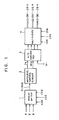
- FIG. 2 designate A/D converters; 5, a color demodulator; 6, a signal processing circuit; 11, a brightness detector consisting of a resistor R1 and a transistor Q1 to detect brightness of image signal; 12, an integrator consisting of resistors R2, R3, a capacitor C1, a diode D1 and a variable resistor VR1; 13, a discharge circuit by a blanking pulse PB consisting of resistors R6, R7 and a transistor Q3; 14, a voltage dividing circuit consisting of resistors R4, R5 and a transistor Q2; R8, R9, R10, voltage dividing resistors; VR2, VR3, VR4, voltage dividing variable resistors; A1, A2, A3, reference voltage output amplifiers; 15, OR gate for logical OR of the most significant bits of the A/D converters 3a, 3b, 3c; D2, D3, D4, reverse current shut-off diodes.
- An image signal input to the input terminal P is first separated to three primary-color signals of R, G, B in the color demodulator and the primary-color signals are then supplied to the A/D converters 3a, 3b, 3c.
- These A/D converters 3a, 3b, 3c convert the R, G, B signals to quantized digital signals.
- the most significant bits of these digital signals, R, G, B are calculated on logical OR in the OR gate 15 and then an output at the OR gate 15 is input to the brightness detector 11 for detection of brightness of image signal. For example, in the case of a dark image signal, the most significant bits of digital outputs of the A/D converters 3a, 3b, 3c are all set to low level. Therefore, the transistor Q1 turns OFF.
- a capacitor C1 of integrator 12 is charged with the voltage set by the variable resistor VR1 and then a base voltage of transistor Q2 is held to this voltage during the one field period of the vertical blanking pulse PB.
- the transistor Q2 turns ON and a voltage determined by the variable resistor VR2, and resistors R4, R5, R8 is supplied to the A/D converter 3a as the reference voltage for example.
- the similar operations are carried out for the A/D converters 3b, 3c. In this case, the resolution of the A/D converters 3a, 3b, 3c virtually increase because the reference voltage becomes lower.
- the output of OR gate 15 becomes high level, the transistor Q1 turns ON and the capacitor C1 is not charged. Accordingly, the transistor Q2 turns OFF and a voltage determined by the variable resistor VR2 and voltage dividing resistor R8 is applied to the A/D converter 3a as the reference voltage input, for example.
- the reference voltages of the A/D converters 3a - 3c can take two kinds of values depending on the quality of image signal input, namely the brightness of the image signal. If the image is dark, the virtual contrast can be raised by setting such two kinds of voltage values to the optimum value and high quality image can be obtained by preventing the saturated black image of display screen.
- the A/D converters 3a - 3c of 4 bits are used but the converters are not limited only to them.
- the present invention has the constitution that the reference voltage of the A/D converter is controlled with the most significant bit output signal of the A/D converter and therefore provides the effect that if an image is dark, the contrast can be adjusted automatically depending on the level of image signal, and thereby saturated black image on the display screen can be prevented and clear and optimum display image can be obtained.
Abstract
Description
- The present invention relates to an improvement of a liquid crystal display device for displaying images of improved contrast ratio.
- Fig. 1 is a block connection diagram indicating a conventional liquid crystal display device disclosed in the Japanese Patent Laid-Open No. 62-188477. In this figure, a
reference numeral 1 designates an analog switch; 2, an autolevel control circuit; 3, an analog/digital converter (hereinafter referred to as A/D converter); 4, a multiplexer working as a signal processing circuit for supplying separated signals of red, green and blue to a drive circuit for image display. - Operations will be explained. In Fig. 1, a video signal input from an input system not illustrated is separated to three primary-color signals of red, green and blue (hereinafter referred respectively as R, G, B) by a color demodulation circuit (not illustrated), these separated analog primary-color signals are time-multiplexed by an
analog switch 1 and these are supplied to anautolevel control circuit 2 as an S-RGB signal. Theautolevel control circuit 2 clamps the S-RGB signal to the lower limit reference voltage Vr-- of the A/D converter 3 and generates an upper limit reference voltage Vr++. Next, a multiplexer as a signal processing circuit separates again the output of the A/D converter into the three primary-color signals of R, G, B. - Though depending on resolution of the A/
D converter 3, a dynamic drive type liquid crystal display device cannot obtain sufficient contrast ratio generally, and therefore it has been in such a tendency as generating a saturated white or black display. Considering such tendency, it is naturally possible to detect the maximum value of the image signal and use such value as the upper limit reference voltage of the A/D converter 3 in order to improve such tendency. However, the three primary-color signals must be time-multiplexed to the one signal by theanalog switch 1. As a result, the prior art has been accompanied by a problem that the analog switch cannot follow the high speed operation in case the resolution of liquid crystal display screen, namely the number of pixels, particularly the number of pixels in the horizontal direction increases. - The present invention has been proposed to overcome such a problem described above and it is a first object to provide a liquid crystal display device which can improve contrast by changing a virtual contrast ratio without using an analog switch.
- It is a second object of the present invention to provide a liquid crystal display device which automatically adjust contrast corresponding to the level of image signal and attain clear and optimum image display even when an image is dark by preventing a saturation of black level on the display screen.
- It is a third object of the present invention to provide a liquid crystal display device which ensures an excellent contrast ratio in comparison with that of the prior art and can be manufactured rather economically than the prior art.
- It is a fourth object of the present invention to automatically compensate for contrast of display screen by utilizing the digital processing technique for image signal.
- In view of attaining the objects of the present invention, the liquid crystal display device of the present invention detects the most significant bit obtained in the output side of an A/D converter with a brightness detector and controls the reference voltage of the A/D converter for the predetermined period using a divided voltage.
- Accordingly, the brightness detector detects the most significant bit of the output of the A/D converter, judges brightness and darkness of image signal based on such detected signal and thereby automatically adjusts contrast of display screen.
- The aforementioned and other objects and a novel feature of the present invention will become apparent by thorough understanding of following detailed explanation with reference to the accompanying drawings. However, the drawings are accompanied only for the convenience of explanation and do not specify the scope of the present invention.
-
- Fig. 1 is a block connection diagram indicating a liquid crystal display device in the prior art.
- Fig. 2 is a block connection diagram indicating the liquid crystal display device as an embodiment of the present invention.
- An embodiment of the present invention will be explained with reference to the accompanying drawings. In Fig. 2, 3a, 3b, 3c designate A/D converters; 5, a color demodulator; 6, a signal processing circuit; 11, a brightness detector consisting of a resistor R1 and a transistor Q1 to detect brightness of image signal; 12, an integrator consisting of resistors R2, R3, a capacitor C1, a diode D1 and a variable resistor VR1; 13, a discharge circuit by a blanking pulse PB consisting of resistors R6, R7 and a transistor Q3; 14, a voltage dividing circuit consisting of resistors R4, R5 and a transistor Q2; R8, R9, R10, voltage dividing resistors; VR2, VR3, VR4, voltage dividing variable resistors; A1, A2, A3, reference voltage output amplifiers; 15, OR gate for logical OR of the most significant bits of the A/D converters 3a, 3b, 3c; D2, D3, D4, reverse current shut-off diodes.
- Operations will be explained below. An image signal input to the input terminal P is first separated to three primary-color signals of R, G, B in the color demodulator and the primary-color signals are then supplied to the A/D converters 3a, 3b, 3c. These A/D converters 3a, 3b, 3c convert the R, G, B signals to quantized digital signals. The most significant bits of these digital signals, R, G, B are calculated on logical OR in the
OR gate 15 and then an output at theOR gate 15 is input to thebrightness detector 11 for detection of brightness of image signal. For example, in the case of a dark image signal, the most significant bits of digital outputs of the A/D converters 3a, 3b, 3c are all set to low level. Therefore, the transistor Q1 turns OFF. In this case, a capacitor C1 ofintegrator 12 is charged with the voltage set by the variable resistor VR1 and then a base voltage of transistor Q2 is held to this voltage during the one field period of the vertical blanking pulse PB. As a result, the transistor Q2 turns ON and a voltage determined by the variable resistor VR2, and resistors R4, R5, R8 is supplied to the A/D converter 3a as the reference voltage for example. The similar operations are carried out for the A/D converters 3b, 3c. In this case, the resolution of the A/D converters 3a, 3b, 3c virtually increase because the reference voltage becomes lower. On the other hand, in the case of a bright image signal, the output ofOR gate 15 becomes high level, the transistor Q1 turns ON and the capacitor C1 is not charged. Accordingly, the transistor Q2 turns OFF and a voltage determined by the variable resistor VR2 and voltage dividing resistor R8 is applied to the A/D converter 3a as the reference voltage input, for example. The reference voltages of the A/D converters 3a - 3c can take two kinds of values depending on the quality of image signal input, namely the brightness of the image signal. If the image is dark, the virtual contrast can be raised by setting such two kinds of voltage values to the optimum value and high quality image can be obtained by preventing the saturated black image of display screen. - In this embodiment, the A/D converters 3a - 3c of 4 bits are used but the converters are not limited only to them.
- As explained previously, the present invention has the constitution that the reference voltage of the A/D converter is controlled with the most significant bit output signal of the A/D converter and therefore provides the effect that if an image is dark, the contrast can be adjusted automatically depending on the level of image signal, and thereby saturated black image on the display screen can be prevented and clear and optimum display image can be obtained.
Claims (2)
Applications Claiming Priority (2)
| Application Number | Priority Date | Filing Date | Title |
|---|---|---|---|
| JP63322106A JPH02168296A (en) | 1988-12-22 | 1988-12-22 | Liquid crystal display device |
| JP322106/88 | 1988-12-22 |
Publications (3)
| Publication Number | Publication Date |
|---|---|
| EP0374372A2 true EP0374372A2 (en) | 1990-06-27 |
| EP0374372A3 EP0374372A3 (en) | 1990-09-12 |
| EP0374372B1 EP0374372B1 (en) | 1994-05-11 |
Family
ID=18139983
Family Applications (1)
| Application Number | Title | Priority Date | Filing Date |
|---|---|---|---|
| EP89116352A Expired - Lifetime EP0374372B1 (en) | 1988-12-22 | 1989-09-05 | Liquid crystal display device |
Country Status (5)
| Country | Link |
|---|---|
| US (1) | US5214418A (en) |
| EP (1) | EP0374372B1 (en) |
| JP (1) | JPH02168296A (en) |
| CA (1) | CA1327855C (en) |
| DE (1) | DE68915257T2 (en) |
Cited By (4)
| Publication number | Priority date | Publication date | Assignee | Title |
|---|---|---|---|---|
| EP0523796A1 (en) * | 1991-07-17 | 1993-01-20 | Philips Electronics Uk Limited | Active matrix display device and its method of operation |
| EP0602623A1 (en) * | 1992-12-18 | 1994-06-22 | NCR International, Inc. | Liquid crystal display device with memory fonction |
| GB2358275A (en) * | 1999-10-05 | 2001-07-18 | Samsung Electronics Co Ltd | Maintaining the average screen light level for a liquid crystal display |
| GB2411536A (en) * | 2004-02-24 | 2005-08-31 | Hitachi Ltd | Sharpness control dependent on image brightness |
Families Citing this family (14)
| Publication number | Priority date | Publication date | Assignee | Title |
|---|---|---|---|---|
| DE69319943T2 (en) * | 1992-02-28 | 1999-02-11 | Canon Kk | Liquid crystal display device |
| US5894127A (en) * | 1996-05-28 | 1999-04-13 | Aluminum Company Of America | Polarized specular reflectance infrared apparatus and method |
| US6483496B2 (en) * | 1998-07-09 | 2002-11-19 | Sanyo Electric Co., Ltd. | Drive circuit for display apparatus |
| CA2363249C (en) | 2000-11-06 | 2005-02-08 | Research In Motion Limited | System and method for achieving optimal display contrast in a mobile communication device |
| JP4170899B2 (en) * | 2001-06-11 | 2008-10-22 | ゲノア・テクノロジーズ・リミテッド | Apparatus, system and method for color display |
| US7714824B2 (en) * | 2001-06-11 | 2010-05-11 | Genoa Color Technologies Ltd. | Multi-primary display with spectrally adapted back-illumination |
| US8289266B2 (en) | 2001-06-11 | 2012-10-16 | Genoa Color Technologies Ltd. | Method, device and system for multi-color sequential LCD panel |
| JP4799823B2 (en) * | 2002-04-11 | 2011-10-26 | ジェノア・カラー・テクノロジーズ・リミテッド | Color display apparatus and method for improving attributes |
| US7471822B2 (en) * | 2002-07-24 | 2008-12-30 | Genoa Color Technologies Ltd | Method and apparatus for high brightness wide color gamut display |
| WO2004068460A1 (en) | 2003-01-28 | 2004-08-12 | Koninklijke Philips Electronics N.V. | Optimal subpixel arrangement for displays with more than three primary colors |
| US7417799B2 (en) * | 2003-08-04 | 2008-08-26 | Genoa Color Technologies Ltd. | Multi-primary color display |
| CN103177701A (en) * | 2003-12-15 | 2013-06-26 | 格诺色彩技术有限公司 | Multi-primary liquid crystal display |
| US7495722B2 (en) | 2003-12-15 | 2009-02-24 | Genoa Color Technologies Ltd. | Multi-color liquid crystal display |
| US8587621B2 (en) * | 2005-11-28 | 2013-11-19 | Genoa Color Technologies Ltd. | Sub-pixel rendering of a multiprimary image |
Citations (3)
| Publication number | Priority date | Publication date | Assignee | Title |
|---|---|---|---|---|
| GB2119593A (en) * | 1982-03-24 | 1983-11-16 | Casio Computer Co Ltd | Video signal analog-to-digital converter for an image display apparatus |
| DE3518433A1 (en) * | 1984-05-22 | 1985-11-28 | Casio Computer Co., Ltd., Tokio/Tokyo | TELEVISION VIDEO SIGNAL A / D CONVERTER DEVICE |
| EP0261901A2 (en) * | 1986-09-20 | 1988-03-30 | THORN EMI plc | Display device |
Family Cites Families (11)
| Publication number | Priority date | Publication date | Assignee | Title |
|---|---|---|---|---|
| JPS5218132A (en) * | 1975-08-01 | 1977-02-10 | Hitachi Ltd | Binary circuit |
| JPS6153908B1 (en) * | 1980-07-25 | 1986-11-19 | Mitsubishi Electric Corp | |
| US4403253A (en) * | 1981-12-28 | 1983-09-06 | General Electric Company | Uniform distribution video processor with controlled reference voltages |
| US4589019A (en) * | 1983-04-22 | 1986-05-13 | Rca Corporation | Digital adder including counter coupled to individual bits of the input |
| JPS59229595A (en) * | 1983-06-13 | 1984-12-24 | ソニー株式会社 | Display driving circuit |
| US4642694A (en) * | 1984-05-22 | 1987-02-10 | Casio Computer Co., Ltd. | Television video signal A/D converter |
| US4642628A (en) * | 1984-06-22 | 1987-02-10 | Citizen Watch Co., Ltd. | Color liquid crystal display apparatus with improved display color mixing |
| US4628362A (en) * | 1985-05-02 | 1986-12-09 | American Dynamics Corporation | Combined video AGC and digitizing circuit |
| GB8623240D0 (en) * | 1986-09-26 | 1986-10-29 | Emi Plc Thorn | Display device |
| KR910003142B1 (en) * | 1986-10-21 | 1991-05-20 | 가시오 게이상기 가부시기가이샤 | Image display apparatus |
| DE3884442T2 (en) * | 1987-04-15 | 1994-02-17 | Sharp Kk | Liquid crystal display device. |
-
1988
- 1988-12-22 JP JP63322106A patent/JPH02168296A/en active Pending
-
1989
- 1989-09-05 US US07/402,779 patent/US5214418A/en not_active Expired - Fee Related
- 1989-09-05 EP EP89116352A patent/EP0374372B1/en not_active Expired - Lifetime
- 1989-09-05 DE DE68915257T patent/DE68915257T2/en not_active Expired - Lifetime
- 1989-09-12 CA CA000611079A patent/CA1327855C/en not_active Expired - Fee Related
Patent Citations (3)
| Publication number | Priority date | Publication date | Assignee | Title |
|---|---|---|---|---|
| GB2119593A (en) * | 1982-03-24 | 1983-11-16 | Casio Computer Co Ltd | Video signal analog-to-digital converter for an image display apparatus |
| DE3518433A1 (en) * | 1984-05-22 | 1985-11-28 | Casio Computer Co., Ltd., Tokio/Tokyo | TELEVISION VIDEO SIGNAL A / D CONVERTER DEVICE |
| EP0261901A2 (en) * | 1986-09-20 | 1988-03-30 | THORN EMI plc | Display device |
Cited By (9)
| Publication number | Priority date | Publication date | Assignee | Title |
|---|---|---|---|---|
| EP0523796A1 (en) * | 1991-07-17 | 1993-01-20 | Philips Electronics Uk Limited | Active matrix display device and its method of operation |
| US5892504A (en) * | 1991-07-17 | 1999-04-06 | U.S. Philips Corporation | Matrix display device and its method of operation |
| EP0602623A1 (en) * | 1992-12-18 | 1994-06-22 | NCR International, Inc. | Liquid crystal display device with memory fonction |
| GB2358275A (en) * | 1999-10-05 | 2001-07-18 | Samsung Electronics Co Ltd | Maintaining the average screen light level for a liquid crystal display |
| GB2358275B (en) * | 1999-10-05 | 2002-01-02 | Samsung Electronics Co Ltd | Apparatus for maintaining average screen light level for ferroelectric liquid crystal display |
| US6603104B1 (en) | 1999-10-05 | 2003-08-05 | Samsung Electronics Co., Ltd. | Apparatus for maintaining average screen light level for ferroelectric liquid crystal display |
| GB2411536A (en) * | 2004-02-24 | 2005-08-31 | Hitachi Ltd | Sharpness control dependent on image brightness |
| GB2411536B (en) * | 2004-02-24 | 2006-04-12 | Hitachi Ltd | Image display method and apparatus |
| US7609282B2 (en) | 2004-02-24 | 2009-10-27 | Hitachi, Ltd. | Image display method and apparatus |
Also Published As
| Publication number | Publication date |
|---|---|
| DE68915257T2 (en) | 1994-12-08 |
| EP0374372B1 (en) | 1994-05-11 |
| CA1327855C (en) | 1994-03-15 |
| DE68915257D1 (en) | 1994-06-16 |
| US5214418A (en) | 1993-05-25 |
| JPH02168296A (en) | 1990-06-28 |
| EP0374372A3 (en) | 1990-09-12 |
Similar Documents
| Publication | Publication Date | Title |
|---|---|---|
| US5214418A (en) | Liquid crystal display device | |
| US5493317A (en) | On-screen display device for a multimode monitor and method thereof | |
| US5555026A (en) | Method and apparatus for stabilizing a video state of a video display having a picture-in-picture function | |
| KR930011182B1 (en) | Contrast correction device for video signal | |
| US5287172A (en) | Automatic on-screen color converting circuit for a color television | |
| GB2148070A (en) | Cathode ray tube drive control circuits | |
| US5764287A (en) | Image pickup apparatus with automatic selection of gamma correction valve | |
| US6188434B1 (en) | Apparatus and method for controlling exposure in a color image pickup device | |
| CA2114256C (en) | Video circuit | |
| US4663668A (en) | Brightness clamping apparatus for TV receiver with multiple inputs | |
| US4860092A (en) | Color image signal processing circuit with white balance control and gain control | |
| US5502508A (en) | Gradation compensating apparatus for a video signal | |
| CN1050955C (en) | Contrast beam current limiting arrangement with secondary brightness beam current limiting provisions | |
| JPH0634510B2 (en) | Automatic white balance adjustment circuit | |
| US20050030430A1 (en) | Video signal processing circuit | |
| EP0637010A1 (en) | Display controller including black signal detector | |
| JP3789658B2 (en) | Analog video signal AD conversion method and plasma display device driving method using the same | |
| JPH0514935A (en) | Level display device for video signal | |
| JPH0652469B2 (en) | Liquid crystal display | |
| KR0148141B1 (en) | Control method of blanking level and its apparatus | |
| KR940011877B1 (en) | Apparatus for making sudder alternations of pictures by intensity of brightness | |
| JPH06292220A (en) | Color signal amplitude limiter for video signal | |
| JPH04296170A (en) | Video signal processing circuit | |
| JPS61251375A (en) | Compression circuit for image pickup signal | |
| JP2522739Y2 (en) | Display device |
Legal Events
| Date | Code | Title | Description |
|---|---|---|---|
| PUAI | Public reference made under article 153(3) epc to a published international application that has entered the european phase |
Free format text: ORIGINAL CODE: 0009012 |
|
| AK | Designated contracting states |
Kind code of ref document: A2 Designated state(s): DE FR GB |
|
| PUAL | Search report despatched |
Free format text: ORIGINAL CODE: 0009013 |
|
| AK | Designated contracting states |
Kind code of ref document: A3 Designated state(s): DE FR GB |
|
| 17P | Request for examination filed |
Effective date: 19900921 |
|
| 17Q | First examination report despatched |
Effective date: 19920825 |
|
| GRAA | (expected) grant |
Free format text: ORIGINAL CODE: 0009210 |
|
| AK | Designated contracting states |
Kind code of ref document: B1 Designated state(s): DE FR GB |
|
| REF | Corresponds to: |
Ref document number: 68915257 Country of ref document: DE Date of ref document: 19940616 |
|
| ET | Fr: translation filed | ||
| PLBE | No opposition filed within time limit |
Free format text: ORIGINAL CODE: 0009261 |
|
| STAA | Information on the status of an ep patent application or granted ep patent |
Free format text: STATUS: NO OPPOSITION FILED WITHIN TIME LIMIT |
|
| 26N | No opposition filed | ||
| PGFP | Annual fee paid to national office [announced via postgrant information from national office to epo] |
Ref country code: GB Payment date: 19950825 Year of fee payment: 7 |
|
| PGFP | Annual fee paid to national office [announced via postgrant information from national office to epo] |
Ref country code: FR Payment date: 19950911 Year of fee payment: 7 |
|
| REG | Reference to a national code |
Ref country code: GB Ref legal event code: 746 Effective date: 19950814 |
|
| PGFP | Annual fee paid to national office [announced via postgrant information from national office to epo] |
Ref country code: DE Payment date: 19950918 Year of fee payment: 7 |
|
| REG | Reference to a national code |
Ref country code: FR Ref legal event code: D6 |
|
| PG25 | Lapsed in a contracting state [announced via postgrant information from national office to epo] |
Ref country code: GB Effective date: 19960905 |
|
| PG25 | Lapsed in a contracting state [announced via postgrant information from national office to epo] |
Ref country code: FR Effective date: 19960930 |
|
| GBPC | Gb: european patent ceased through non-payment of renewal fee |
Effective date: 19960905 |
|
| PG25 | Lapsed in a contracting state [announced via postgrant information from national office to epo] |
Ref country code: DE Effective date: 19970603 |
|
| REG | Reference to a national code |
Ref country code: FR Ref legal event code: ST |
|
| REG | Reference to a national code |
Ref country code: FR Ref legal event code: ST |