EP0372420A2 - Magnetic recording-reproducing apparatus and magnetoresistive head for use therewith - Google Patents
Magnetic recording-reproducing apparatus and magnetoresistive head for use therewith Download PDFInfo
- Publication number
- EP0372420A2 EP0372420A2 EP89122218A EP89122218A EP0372420A2 EP 0372420 A2 EP0372420 A2 EP 0372420A2 EP 89122218 A EP89122218 A EP 89122218A EP 89122218 A EP89122218 A EP 89122218A EP 0372420 A2 EP0372420 A2 EP 0372420A2
- Authority
- EP
- European Patent Office
- Prior art keywords
- magnetoresistive
- magnetic
- films
- film
- recording medium
- Prior art date
- Legal status (The legal status is an assumption and is not a legal conclusion. Google has not performed a legal analysis and makes no representation as to the accuracy of the status listed.)
- Granted
Links
Images


Classifications
-
- G—PHYSICS
- G11—INFORMATION STORAGE
- G11B—INFORMATION STORAGE BASED ON RELATIVE MOVEMENT BETWEEN RECORD CARRIER AND TRANSDUCER
- G11B5/00—Recording by magnetisation or demagnetisation of a record carrier; Reproducing by magnetic means; Record carriers therefor
- G11B5/127—Structure or manufacture of heads, e.g. inductive
- G11B5/33—Structure or manufacture of flux-sensitive heads, i.e. for reproduction only; Combination of such heads with means for recording or erasing only
- G11B5/39—Structure or manufacture of flux-sensitive heads, i.e. for reproduction only; Combination of such heads with means for recording or erasing only using magneto-resistive devices or effects
- G11B5/3903—Structure or manufacture of flux-sensitive heads, i.e. for reproduction only; Combination of such heads with means for recording or erasing only using magneto-resistive devices or effects using magnetic thin film layers or their effects, the films being part of integrated structures
-
- G—PHYSICS
- G11—INFORMATION STORAGE
- G11B—INFORMATION STORAGE BASED ON RELATIVE MOVEMENT BETWEEN RECORD CARRIER AND TRANSDUCER
- G11B5/00—Recording by magnetisation or demagnetisation of a record carrier; Reproducing by magnetic means; Record carriers therefor
- G11B5/02—Recording, reproducing, or erasing methods; Read, write or erase circuits therefor
- G11B5/09—Digital recording
-
- G—PHYSICS
- G11—INFORMATION STORAGE
- G11B—INFORMATION STORAGE BASED ON RELATIVE MOVEMENT BETWEEN RECORD CARRIER AND TRANSDUCER
- G11B5/00—Recording by magnetisation or demagnetisation of a record carrier; Reproducing by magnetic means; Record carriers therefor
- G11B5/127—Structure or manufacture of heads, e.g. inductive
- G11B5/33—Structure or manufacture of flux-sensitive heads, i.e. for reproduction only; Combination of such heads with means for recording or erasing only
- G11B5/39—Structure or manufacture of flux-sensitive heads, i.e. for reproduction only; Combination of such heads with means for recording or erasing only using magneto-resistive devices or effects
- G11B5/3903—Structure or manufacture of flux-sensitive heads, i.e. for reproduction only; Combination of such heads with means for recording or erasing only using magneto-resistive devices or effects using magnetic thin film layers or their effects, the films being part of integrated structures
- G11B5/3906—Details related to the use of magnetic thin film layers or to their effects
- G11B5/3945—Heads comprising more than one sensitive element
- G11B5/3948—Heads comprising more than one sensitive element the sensitive elements being active read-out elements
-
- G—PHYSICS
- G11—INFORMATION STORAGE
- G11B—INFORMATION STORAGE BASED ON RELATIVE MOVEMENT BETWEEN RECORD CARRIER AND TRANSDUCER
- G11B5/00—Recording by magnetisation or demagnetisation of a record carrier; Reproducing by magnetic means; Record carriers therefor
- G11B5/127—Structure or manufacture of heads, e.g. inductive
- G11B5/33—Structure or manufacture of flux-sensitive heads, i.e. for reproduction only; Combination of such heads with means for recording or erasing only
- G11B5/39—Structure or manufacture of flux-sensitive heads, i.e. for reproduction only; Combination of such heads with means for recording or erasing only using magneto-resistive devices or effects
- G11B5/3903—Structure or manufacture of flux-sensitive heads, i.e. for reproduction only; Combination of such heads with means for recording or erasing only using magneto-resistive devices or effects using magnetic thin film layers or their effects, the films being part of integrated structures
- G11B5/3967—Composite structural arrangements of transducers, e.g. inductive write and magnetoresistive read
-
- G—PHYSICS
- G11—INFORMATION STORAGE
- G11B—INFORMATION STORAGE BASED ON RELATIVE MOVEMENT BETWEEN RECORD CARRIER AND TRANSDUCER
- G11B5/00—Recording by magnetisation or demagnetisation of a record carrier; Reproducing by magnetic means; Record carriers therefor
- G11B5/48—Disposition or mounting of heads or head supports relative to record carriers ; arrangements of heads, e.g. for scanning the record carrier to increase the relative speed
- G11B5/488—Disposition of heads
- G11B5/4886—Disposition of heads relative to rotating disc
Definitions
- the present invention relates to magnetic recording-reproducing apparatus used in auxiliary storage of computers, and magnetic heads for use therewith, and more particularly to superhigh recording density magnetic recording-reproducing apparatus and magnetic heads suitable for magnetic recording and reproduction with a narrow recording track.
- magnetic discs of current commercially available magnetic recording-reproducing apparatus have a linear recording density of about 25 KBPI, a track density of about 1.5 KTPI and an area recording density of about 35 Mb/in2.
- the magnetic heads used for these magnetic discs are inductive thin film heads.
- One such head records and reproduces an information signal.
- it seems that the use of a composite magnetic head which separately includes a recording magnetic head and a reproducing magnetic head will be required in the magnetic recording-reproducing apparatus in the future.
- Known conventional composite magnetic heads use the reproducing head of a magnetoresistive (MR) type using a soft-magnetic thin film magnetoresistive effect, as disclosed in Japanese Patent Publication JP-A-51-44917.
- Other conventional MR heads are ones where the direction of a sense current which flows through the MR element and the direction of the signal magnetic field from a medium are normal to each other, as disclosed, for example, in IEEE, Trans. Magnetics, HAG-7, No. 1 (1971) pp. 150 - 154.
- JP-A50-65211 discloses an MR head of the type which includes two juxtaposed such MR elements with bias magnetic fields which are gnerated from current magnetic fields produced by currents flowing through both the MR elements and differentially amplify the output voltages from both the MR elements.
- JP-A-52-14381 discloses an MR head where the direction of the sense current flowing through the MR element and the direction of the signal magnetic field from a medium are parallel and electrodes are formed on a medium facing surface and an opposite surface of the MR film.
- JP-A61-182620 and 62-234218 disclose an MR head where the direction of the sense current flowing through an MR element and the direction of the signal magnetic field from a medium are parallel and where two MR films are connected electrically in parallel to use magnetic fields produced by currents flowing through both the MR films in the same direction to form a single magnetic domain in the MR films, and to reduce Barkhausen noise.
- the differential amplification type MR head disclosed in the above Publication JP-A-50-65211 is influenced by a signal magnetic field from the adjacent track because the medium facing edge of the MR film is considerably large in width compared to the track to thereby increase noise. Since it takes different times for the two superimposed MR films to absorb the signal magnetic fields, the output waveform obtained by differentially amplifying the outputs from the MR elements is greatly distorted disadvantageously.
- the MR heads disclosed in Japanese Patent Publications JP-A-61-182620 and 62-234218 have MR films which are connected electrically in parallel with electrodes being provided on the medium facing surface side of the MR film which is most sensitive to the signal magnetic field, so that the intensity of the resulting output signal corresponding to the signal magnetic field is low or noise due to temperature fluctuations cannot be removed. Thus, the signal to noise ratio is reduced further as the track width becomes narrower.
- the pesent invention provides a magnetoresistive effect magnetic head comprising: means for introducing magnetic flux from a recording medium into the head; means for dividing the introduced magnetic flux midway in a flux path; and a magnetoresistive effect film for detecting the divided flux.
- the magnetic flux is introduced through a Y- or V-like magnetoresistive effect film, and divided midway and detected.
- a magnetic recording-reproducing apparatus comprises: a recording inductive magnetic head; a reproducing magnetoresistive effect magnetic head; a read-write circuit for inputting a signal to the inductive magnetic head and for reproducing the output from the magnetoresistive magnetic head; an interface for inputting/outputting a signal between the read-write circuit and a superior device; and means for moving the inductive magnetic head, magnetoresistive effect magnetic head and the magnetic recording medium relative to one another, wherein the information recorded on the recording medium is reproduced with an area recording density of 300 Mb/in2 or more.
- a magnetoresistive effect magnetic head comprises: two magnetoresistive effect films connected electrically and magnetically to a recording medium facing surface of the head; and means for differentially amplifying the outputs from the magnetoresistive effect films.
- a magnetoresistive effect magnetic head comprises:
- two magnetic shield layers disposed at a space of about 0.7 ⁇ m; two or more magnetoresistive effect times superimposed between the magnetic shield layers; and means for differentially amplifying the outputs from the two or more magnetoresistive effect films.
- a magnetoresistive effect device comprises: a magnetoresistive effect film for detecting a signal magnetic field from a magnetic recording medium; means for applying a bias magnetic field to the magnetoresistive effect film; a pair of conductors for causing an electric current to flow through the magnetoresistive effect film to read the voltage across the magnetoresistive effect film; a pair of magnetic shield members for magnetically shielding the magnetoresistive effect film, wherein the magnetoresistive effect film includes; two magnetoresistive effect subfilms connected in series and having positive and negative ⁇ effects in response to a magnetic field applied thereto.
- the direction of a sense current flowing through the MR element and the direction of a signal from a medium are parallel.
- the MR film section which reads the signal magnetic field from the medium has a multilayered structure with electrodes on the respective surface of the MR films facing the medium and on the opposite sides of the films such that the voltage across the electrodes is differentially amplified and withdrawn as an output signal.
- at least two inner layers of the multilayered MR film are combined magnetically and electrically on the medium facing side of the head.
- a current lead is provided between the MR films.
- the thickness and width of the MR film on the medium facing surface are set to 0.1 ⁇ m or less and 4 ⁇ m or less, respectively, and the spacing between an upper and a lower magnetic shield layer in the MR head is controlled so as to be 0.7 ⁇ m or less.
- MR films of the multilayered MR element are connected in series at their ends on side of the medium facing surface of the head electrically and magnetically so as to provide an output.
- the MR film structure has a multilayered one, the voltage generated across the electrodes provided on the surfaces of the MR films facing the medium and on the opposite sides of the MR films are differentially amplified.
- modulation noise due to fluctuations in the ambient temperature are cancelled, and the intensity of the output signal is increased compared to a magnetic head using a single MR film.
- At least two inner films of the multilayered MR element are coupled magnetically and electrically on the side of the medium facing surface of the head to thereby eliminate the difference between the times when the signal magnetic field from the medium is absorbed by the combined MR films.
- a current lead provided between the MR films provides a magnetic field generated by a current flowing through the current lead and acts so as to bias by any quantity in opposite directions the directions of magnetization in the MR films positioned above and below the current lead.
- At least two inner films of the multilayered MR element are connected magnetically and electrically on the side of the medium facing surface of the head. Electrodes are provided on the MR films opposite to the medium facing sides of the respective combined MR films such that a sense current flows across the electrodes to provide an output signal.
- the overall resistance between the electrodes is the sum of the respective resistances of the MR films since the respective MR films are connected in series. Therefore, if the currents flowing the MR films are arranged so as to be the same, the voltage across the electrodes is twice as high as that generated by a head using a single MR film, and hence the intensity of the output signal corresponding to the signal magnetic field applied to the head is twice as high as that obtained by the head using the single MR layer.
- the MR films which produces a positive and a negative ⁇ effect are arranged in series, so that the differential effect is realized although two terminals are used.
- wiring is easy also in narrow tracks.
- FIG. 2 schematically illustrates a magnetic disc storage system having a recording density of 300 Mb/in2 or more as a first embodiment of the present invention.
- the main mechanism includes a recording medium 100, a magnetic head 101, an actuator 102 and a spindle motor 103.
- Magnetic head 101 is connected via an interface 107 to a read-write circuit 104, a positioning circuit 105 and a control circuit 106.
- Digital information and a control signal are input to the disc storage device via interface 107.
- the linear recording density is 75 kBPI (the bit length is 0.43 ⁇ m)
- the track density is 4 kTPI (the track width is 4 ⁇ m).
- Recording medium 100 includes a Co sputted medium of a coercivity of 2000 oerstead or more.
- Magnetic head 101 includes of a composite type having separate recording and reproducing functions which will be described in more detail later with reference to FIG. 1.
- Actuator 102 is controlled by positioning circuit 105 with a positioning accuracy of 0.5 ⁇ m.
- the spacing between recording medium 100 and magnetic head 101 is 0.1 - 0.15 ⁇ m.
- the rotation of spindle motor 103 is controlled by power source control circuit 108 so as to drive a disc-like medium.
- FIG. 1 is a cross-sectional perspective view of the magnetic head.
- the head is a recording-reproducing spearation type head which includes a reproducing section-recording section superimposed on a substrate in which a differential MR head of two layered MR elements is used for reproduction and in which an inductive head is used for recording.
- the reproducing track and recording track are 3 ⁇ m and 4 ⁇ m, respectively, in width.
- the spacing between the shielding layers is required to be at least a minimum bit period or less. As shown below, in the particular embodiment, the spacing between the shielding layers is 0.68 ⁇ m, which corresponds to a bit period of about 100 kBPI.
- a method of preparing such head will now be described in detail.
- a non-magnetic substrate 1 for example, of ceramics
- an insulator 2 such as alumina or silica
- a substrate of a soft magnetic material such as ferrite may be used which also functions as a lower magnetic shield.
- An insulator film 4 having a thickness of 0.1 - 0.4 ⁇ m using sputtering. While alumina or silica may be used as the insualting layer, alumina was used as the materials of the insulator layers of all the embodiments of the present invention to be described later.
- the spacing between the shield layer and MR elements formed later is determined by the thickness of the insulator. as described above, the spacing influences the resolution of the recording and reproducing characteristic, so that it must be selected depending on the recording density of the head.
- the thickness of the insulator was 0.2 ⁇ m.
- a conductor 5 as an electrode terminal for a first MR element is formed.
- the material of the conductor 5 may be made of a material of high conductivity such as Al or Cu. In the particular embodiment, all the conductors and conductive layers to be described later was Cu. The thickness of the conductor is 0.3 ⁇ m and the pattern of the conductor 5 was formed by regular photolithographic techniques.
- an MR film of Ni-Fe alloy or Ni-Co alloy so as to be 10 - 100 nm using evaporation or sputtering. Then photoetching was used to form a first MR element 6 having a predetermined shape.
- the first MR element was 3 ⁇ m broad and three times as long as the track width to reduce the influence of a demagnetizing field.
- the thickness of the MR film also influences the demagnetizing field. If the demagnetizing field is strong, the dynamic range of the magnetic field of an input signal is expanded, but the head sensitivity is reduced. In the particular embodiment, the magnitude of the residual magnetization in a medium used and the head sensitivity are considered so that the film thickness of the MR element is set to 40 nm.
- the magnetic-easy direction of the MR film was set so as to be across the track.
- an insulator film 7 and then a conductor pattern 8 were formed and an insulator layer 9 was deposited.
- the insualtor layers 7, 9 and conductor layer 8 each were 0.2 ⁇ m thick.
- the insualtor layer on an end of the MR element on the medium facing side of the head was etched away to form a through hole to thereby expose a portion of the first MR element.
- An MR film was then deposited and worked on the same conditions as the previous MR element to form a second MR element 10 which was connected with the first MR element at the through hole. What is important in this process is that the first and second MR elements 6 and 10 are securedly connected at one end electrically and magnetically and that both the elements have the same characteristics. While in the particular embodiment the two RM elements are directly connected at one end, the elements may be connected via a soft magnetic film provided therebetween.
- a 0.2- ⁇ m thick electrode film was then deposited and worked to form electrode patterns 11 and 12 at the corresponding ends of the second MR element. Subsequently, a 0.2- ⁇ m insulator film 13 was desposited, and, as an upper magnetic shield layer 14, a 1- ⁇ m Ni-Fe alloy soft magnetic film was deposited.
- a 3- ⁇ m insulator film 15 was then deposited, the surface of which was then flattened using etch-back method.
- a 3- ⁇ m Co amorphous soft magnetic film was deposited as a lower magnetic pole 16 for the recording head under a saturated magnetic flux density of 1.5 Teslas. Regular photoetching was then conducted to form the magnetic pole 16 of a predetermined shape.
- the track width of the lower magnetic pole was 4.5 ⁇ m.
- Deposited as a gap layer between the recording magnetic poles was a 2- ⁇ m insulator film 17.
- a through hole 18 was then formed in the back contact section. Thereafter, a coil pattern 19 was formed in a 2- ⁇ m thick conductive layer.
- a flat resin layer 20 and then an upper magnetic pole 21 were formed on conditions similar to those for the lower magnetic pole.
- the width of a track in the upper pole was 4 ⁇ m.
- the sense currents flowing through the two-MR elements have the same direction, so that the MR elements are magnetized in opposite directions of track traverse due to magnetic fields formed by the currents. Therefore, magnetostatic coupling is effected between the MR elements to thereby establish a stabilized magnetic structure.
- the respective elements can have the directions of their magnetization at an angle of about 45 degrees to the direction of track traverse to thereby improve the linearity and sensitivity of the output while a stable magnetic domain structure is being maintained.
- the signal flux entering the magnetic electrical junction of the element ends diverges into the MR elements and the magnetization is rotated such that the resistance to the flux in one element increases while the resistance to the flux in the other element decreases. Therefore, the outputs from electrodes provided at the leading and trailing ends of the elements can be amplified differentially, and the resulting output is twice as high as the output from a single MR element.
- the differential amplification serves to eliminate part of modulation noise, for example, due to temperature fluctuations.
- the linearity of the output in response to the input magnetic field is improved to thereby expand the dynamic range.
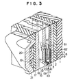
- FIG. 3 illustrates the head of two MR films one including a pair of two MR films 61 and 62 and insulator layer 41 therebetween and the other including a pair of two MR films 101 and 102 and insulator layer 131 therebetween where the inner MR films 61, 101 are connected at one end such that electrode terminals 5, 11 and 12 supply electric currents to the MR films.
- the outer MR films 62, 102 are magnetized by magnetic fields produced by the sense currents flowing through the inner MR films to thereby apply to the inner MR films bias magnetic fields having directions of track traverse. Therefore, the directions of magnetization of the inner MR films are stabilized to thereby prevent the generation of an unstable magnetic domain structure which would otherwise generate Barkhausen noise.
- the insulator layers are preferably thin, but were selected to be 50 nm thick from a standpoint of electrical insualtion.
- the shape of the MR element is similar to that of the first embodiment. As in the first embodiment, the currents flowing through the first and second MR elements apply bias magnetic fields similar to those in the first embodiment to thereby stabilize the magnetic domain structure.
- the magnetic domain structure is stabilized more efficiently. While in the particular embodiment the outer film 62, 102 are only required to be a soft magnetic film, so that they may be another appropriate material.
- a third embodiment of FIG. 4 is intended to reduce a stray field entering from the MR films to a shield layer.
- the distance between the shield layer and the MR films was selected to be large except in the vicinity of the medium facing surface of the device.
- the head was fabricated as follows. First, a 2- ⁇ m deep recess was formed having a tapered side in a substrate side and a shield layer 3 was then formed. An insualtor layer 4 was then deposited so as to be 3 ⁇ m or more thick and flattened using etch-back method. Subsequently, like the first embodiment, two MR films 6 and 10 and a conductor 8 were formed. The shape of the MR films were similar to those of the first embodiment.
- An insulator layer 15 was then deposited so as to be 2 ⁇ m or more thick and then the insulator layer was removed at an end of the device on the medium facing side. Thereafter, an insualtor film 151 was deposited over so as to be 0.2 ⁇ m thick and a soft magnetic film functioning as shield layer 14 and lower magnetic pole 16 was formed on the insualtor film 151.
- Co amorphous alloy was employed as the soft magnetic film.
- etch-back method was used. In consideration of a decrease in the film thickness due to etch-back, the thickness of the magnetic film was set to 4 ⁇ m.
- insulator layer 17, coil 19, flattened layer 20, and upper magnetic pole 21 were formed to constitute the recording head section on the same conditions as those mentioned above.
- the reproduced output from the such head increased by about 30% compared to the first embodiment.
- the S/N ratio was improved and the formation of narrow tracks was effected successfully.
- FIG. 5 illustrates the head structure.
- the reproducing section includes two MR films 6 and 10 which are connected in series to thereby provide an output comprising the sum of both the outputs from the MR films.
- electrode terminals are not provided on the medium facing surface of the MR films, but only at ends of the MR films on the opposite side of the head from its medium facing surface.
- the head was fabricated as follows. Up to the first MR film were prepared using a process similar to that employed in the formation of the first embodiment, and subsequently, insulator layer 7 was formed. A 0.2- ⁇ m thick Co-Pt film was then deposited and processed to form a permanent magnet film pattern 22. As described later, the pattern was used to generate a bias magnetic field. Subsequently, a second MR film was formed via an insulator layer 9. Electrode 12 was then formed on an end of the MR film. Thereafter, like the formation of the first embodiment, insulator layer 13, and shield layer 14 were formed, and then a recording section was formed. After the formation of the head, a direct current magnetic field was applied to the head in a direction perpendicular to the width of the tracks for magnetizing as the permanent magnet.
- both the MR films were connected in series, the sense currents from the MR films had opposite directions, so that by the magnetic fields generated by both the currents both the MR films were magnetized in the direction where they traversed the tracks.
- the permanent magnet film 22 provided between both the films applies a bias magnetic field across each of the films in the same direction. Further, the signal magnetic field from a medium rotates the magnetization of the films in the same direction. Therefore, both the MR films exhibit the same change in resistance in response to the signal magnetic field applied thereto.
- the output from the electrodes 5 and 12 connected in series is twice as high as that in a single element.
- the particular embodiment provides a high output comprising the sum of both the outputs.
- the magnitude of the bias depends on the thickness of the permanent magnet and the magnitude of the sense current, so that an appropriate magnet thickness should be selected.
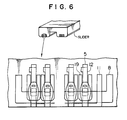
- FIG. 6 schematically illustrates a fifth embodiment of a recording-reproducing apparatus which comprises a multi-track head device which includes a plurality of composite heads of recording-reproduction separating type provided on a single slider.
- the main mechanical portion of the recording-reproducing device includes a recording medium, the magnetic head, actuator and spindle motor and is connected to an interface for a computer via a read-write circuit for a multi-track, a positioning circuit and a power source control unit.
- the linear recording density is 75 kBPI (the bit length is 0.43 ⁇ m) and the track density is 4 kTPI (the track width is 4 ⁇ m).
- FIG. 6 is a perspective view of a multi-track magnetic head used and an enlarged plan view of the head portion.
- a plurality of heads are formed on a rail on each side of the slider.
- the pitch of the head is required to be an integer times the track pitch in order to use the recroding medium surface effectively. In the particular embodiment, the pitch is twice the track pitch.
- electrode 11 for the MR film on the medium facing surface side and conductive pattern 8 formed between the two MR films are used in common. Electrodes 5, 12 for the MR films; recording magnetic poles 16, 21; and coil 19 on the opposite side of the disc from the medium facing surface are provided in each head.
- a recording density similar to that obtained by the first embodiment is realized. Since a plurality of data can be recorded and reproduced simultaneously, the data transfer rate is greatly improved.
- a conventional magnetoresistive element includes a separate soft magnetic thin film provided in a magnetic field active region of the element provided spaced from the medium facing surface in order to guide signal magnetic flux from a magnetic recording medium, as disclosed in Japanese Patent Publication JP-A-63-18506.
- JP-A-63-18506 an insulator layer is provided between the soft magnetic thin film for guide of the signal flux and the magnetic field active region of the magnetoresistive film, so that the magnetic resistance between these films increases to reduce a quantity of signal flux introduced in the magnetic field active region. Therefore, the signal reproducing efficiency of the magnetoresistive element is low disadvantageously.
- a magnetoresistive film itself extended to the recording medium facing surface and took a shape extending in the form of a strip from the medium facing surface. Current leads were then formed sequentially spaced from the medium facing surface.
- FIG. 7a is a front view of a magnetoresistive element according to one embodiment of the present invention.
- FIG. 7b is a cross section view taken along the line A-A′ of FIG. 7a.
- An insulator layer 2 of Al2O3 or SiO2 was deposited so as to be 0.1 - 0.4 ⁇ m, for example, using sputtering, on a substrate 1 which also functioned as a lower magnetic shield of a magnetic material such as ferrite (the substrate may include a soft magnetic thin film for the lower magnetic shield desposited on a non-magnetic material, for example, of ceramics via an insulator layer, for example, of Al2O3).
- a conductive film 8 of a good conductor such as Al, Cu, Nb or Ti was deposited on the insulator layer 2 using evaporation or sputtering to apply a bias magnetic field to a magnetic field active region 600 of magnetoresistive film 6. Then, patterning was effected so as to provide a predetermined shape using photolithography and dry or wet etching.
- Magnetoresistive film 6 for example, of Ni-Fe alloy or Ni-Co alloy was deposited so as to be 10 - 100 nm thick using evaporation or sputtering via a 0.1 - 0.2 ⁇ m thick insulator layer 9 of the same material as insulator layer 2. Photolithography and dry etching were then used to provide a predetermined patterned shape. Magnetoresistive film 6 is equal in width to a track on magnetic recording medium 100 and has a length equal to three times the width of the track to reduce the influence of demagnetizing field.
- the magnetic easy direction of magnetoresistive effect film 6 was selected so as to be the shorter-axis direction of the pattern.
- Signal sense current introducing leads 81, 12 of Al, Cu, Nb or Ti were sequentially formed spaced from recording medium facing surface 900 on magnetoresistive film 6.
- the distance from recording medium facing surface 900 to current guide lead 81 is required to be larger than the maximum quantity of abrasion produced when the magnetoresistive element is operated over magnetic recording medium 100.
- the spacing between current introducing leads 12′ and 81 is required to be the track width or more in consideration of the output from the magnetoresistive element 120. It is preferable that the distance from the recording medium facing surface to current introducing lead 81 should be appropriately selected depending on a device using the particular embodiment.
- the distance is preferably 1 - 10 ⁇ m.
- the distance should be selected so as to increase the quantity of abrasion by +2 - 5 ⁇ m.
- the width of the magnetoresistive film is preferably small.
- a magnetoresistive element 120 was prepared by depositing a 0.1 - 0.8- ⁇ m thick insulator film 13 of Al2O3 or SiO2 and then a 0.3 - 3- ⁇ m thick soft magnetic thin film 14 of permalloy for the upper magnetic shield (or bonding a soft magnetic material of ferrite with an additive).
- the signal flux 130 leaking out from magnetic recording medium 100 enters magnetoresistive film 6 exposed on the medium facing surface 900 to be led to magnetic field active region 600, which senses a change in the voltage corresponding to a change in the resistance of the magnetic field active region from the sense current introducing leads 12, 81 using the fact that the resistance of the magnetic active section 600 changes depending on the magnetoresistive effect by the signal flux introduced into the magnetic field active region.
- the signal indicative of records on the magnetic recording medium 100 is read.
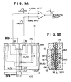
- FIGs. 8a and 8b illustrate the operational principle of the magnetoresistive element 120.
- FIG. 8a illustrates the magnetization of magnetoresistive film 6 while
- FIG. 8b illustrates an external magnetic field 6 response curve on the output from magnetoresistive element 120.
- magnetoresistive film 6 of the particular embodiment several magnetic domains are formed in which the directions of magnetization M in adjacent magnetic domains are parallel, and perpendicular to the direction of current I, as shown in FIG. 8a.
- the external magnetic field response curve on the output from the element obtained when an alternating magnetic field H is applied to the element so as to be parallel to the direction of current I is such that when the external magnetic field H increases in any of the senses of + and - the output increases parabolically.
- signal flux 130 is directly guided from mangetoresistive film 6 exposed on medium facing surface 900 to magnetic field active region 600. Furthermore, the influence of the demagnetizing field in the longer pattern axis of magnetoresistive film 6 is very small, so that the quantity of signal magnetic flux entering the medium facing surface 900 is guided without decrease due to leakage to the magnetic field active region 600. Thus, the output from the element 120 is enhanced compared to the conventional device.
- FIG. 9a is a front view of a magentoresistive element according to another embodiment of the present invention.
- FIG. 9b is a cross-sectional view taken along the line B-B′ of FIG. 9a.
- a groove 14 was formed to provide sense current leads 81 in insulator layer 2 deposited on a substrate 1 using dry etching such as photolithography and ion milling.
- Current guide leads 81 of Al, Cu, Nb or Ti were then embedded in groove 814.
- magnetoresistive film 51 of Ni-Fe alloy or Ni-Co alloy was deposited so as to be 10 - 100 nm thick using evaporation or sputtering.
- patterning was effected so as to provide a shape similar to that obtained in the embodiment 6 using similar processes.
- current lead 81 and magnetoresistive film 51 were put in contact with each other in a conductive state.
- Insulator layer 815 of the same material as insulator layer 2 was then deposited so as to be 0.05 - 0.2 ⁇ m thick.
- Conductive film 8 for application of bias magnetic field was prepared similarly to embodiment 6. At this time, the edges of conductive film 8 were inclined at an angle of 20 - 60 degrees to improve coverage.
- insulator layer 816 of the same material as insulator layers 2, 815 was deposited so as to be 0.05 - 0.2 ⁇ m thick.
- the second magnetoresistive film 52 was prepared so as to have the same thickness and shape as the first magnetoresistive film 51 using similar processes.
- first and second magnetoresistive films 52 and 51 are put into contact with each other on, or close to, medium facing surface 900.
- the magnetic-easy directions of the first and second magnetoresistive films are set so as to be the same. In this case, they may be parallel to either the shorter pattern axis or the longer pattern axis. Preferably, they are parallel to the shorter pattern axis.
- Sense current leads 82 were provided on the second magnetoresistive film 52.
- through hole 818 was also provided in insulator layers 815 and 816 so as to short-circuit the medium facing surface side of the sense current guide lead 82 and the sense current leads 81 on the medium facing surface side underlying the first magnetoresistive film 51. While the upper and lower current leads on the medium facing surface side are short-circuited, the current leads on the opposite side of the head from the medium facing surface side may be short-circuited instead.
- the distance between the medium facing surface 900 and the current leads and the distance between the current leads are preferably equal for the upper and lower current leads 82 and 81, and similar to the distances for the current leads in embodiment 6 and should be set to an approriate value depending on a device using the particular embodiment as in the embodiment 6.
- the width of magnetoresistive films 51 and 52 are preferably small.
- insulator layer 810 was deposited and upper magnetic shield layer 811 was formed to provide a magnetoresistive element 120.
- the magnetoresistive element 120 of the particular embodiment is characterized in that instead of the single magnetoresistive film 6 of magnetoresistive element 120 of embodiment 6, two magnetoresistive films are used and that the upper and lower magnetoresistive films are put into contact with each other on the medium facing surface and in its vicinity.
- the magnetoresistive films 51 and 52 exposed on the medium facing surface 900 receive signal flux 130 simultaneously and guides it to the magnetic field active regions 61 and 62 on the upper and lower magnetoresistive films.
- FIG. 9a illustrates the diferential amplifier which receives output voltages at signal input terminals + and - thereof from current leads 81 and 82 and provides the output signal as the differential amplification of the output voltages from the signal output terminals.
- Changes in the resistance values of the magnetic field active regions 61 and 62 are equal because, as mentioned above, the same quantity of signal flux enters each of the magnetic field active regions 61 and 62, so that changes in the voltages detected by current leads 81 and 82 are equal in correspondence to changes in the respective resistance values of magnetic field active regions 61 and 62.
- the signal flux entering simutlaneously from the medium facing surface 900 to magnetoresistive films 51 and 52 arrive simultaneously at magnetic field active regions 61 and 62. Therefore, the phases of changes in the respective voltages detected by current lead 81 and 82 are the same and no phase difference will occur.
- the direction of the bias magnet field is opposite to each of the upper and lower magnetoresistive films to thereby permit to amplify the respective output voltages differentially. Even if conductive film 8 is not provided between the magnetoresistive films, one conductive film 8 may be provided for applying a bias magnetic field to each of the magnetoresistive films.
- the same quantity of signal magnetic flux is guided to each of the magnetic field active regions of the upper and lower magnetoresistive films simultaneously, in addition to effects similar to those of embodiment 6, mentioned above. Therefore, even if the output voltages from the magnetic field active regions are amplified differentially, the resulting differentially amplified waveform is not distorted and high output is provided.
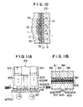
- FIG. 10 is a cross sectional view of a magnetoresistive element according to a further embodiment of the present invention in which a single common current lead replaces the upper and lower current leads, either on the medium facing surface 900 side or on its opposite side, of sense current guide leads 81 and 82 formed on the upper and lower magnetoresistive films 51 and 52 in the magnetoresistive element 120 of embodiment 7.
- FIG. 11 illustrates the use of a common current lead on the medium facing surface 900 side.
- the other remaining structure is quite the same as that of embodiment 7 and the operation and advantages of the particular embodiment are similar to those of embodiment 7.
- the signal flux leading out from a magnetic recording medium can be guided to the magnetic field active regions of the magnetoresistive element without being reduced, so that the output from the magnetoresistive element is enhanced. Further, the same quantity of signal magnetic flux can be guided simultaneously to each of the magnetic field active regions of the two-layered magnetoresistive element so that when the output voltages from the magnetic field active regions are amplified differentially, the resulting differentially amplified waveform is not distorted. Therefore, a magnetoresistive element of higher output is provided. According to the particular embodiment, since the magnetoresistive films extend in the form of a strip from the medium facing surface, the output does not greatly decrease even if the track width becomes very narrow. Therefore, the effect produced by the present invention is more greatly exhibited as the track width becomes narrower.
- a conventional magnetoresistive element using a soft magnetic film as bias magnetic field applying means includes two conductors, one on each end of a magnetoresistive film.
- the output from the magnetoresistive element exhibits a parabolic output in response to external magnetic field applied to the element.
- Japanese Patent Publication JP-A-61-199684 proposes a bias type magnetoresistive element which is intended to expand its dynamic range and to reduce noise, and which uses a soft magnetic thin film where the two parabolic magnetoresistive element outputs disclosed in the Publication '213 are amplfiied differentially.
- the magnetoresistive element includes three conducors; a common conductor at the center of the magnetoresistive film thereof for differentiating purposes and two further conductors, one provided on each end of the magnetoresistive film.
- the magnetoresistive element disclosed in the Publication '213 is advantageous for a magnetic recording medium having narrow tracks because the two conductors are used, but it provides a parabolic output, so that the dynamic range is narrow disadvantageously.
- the dynamic range is wide advantageously, it is very difficult to prepare a magnetoresistive element having three conductors and dealing with narrowing tracks in the magnetic recording medium.
- a magnetoresistive film structure used in the magnetoresistive element includes series connected magnetoresistive films having a positive and a negative ⁇ effect in response to magnetic field applied thereto, both the positive and negative ⁇ effects being the same in magnitude, and two conductors connecting both ends of the joined films.
- bias applying means such as soft magnetic films are provided in contact with, or close to, the respective magnetoresistive films in facing relationship on the opposite positions in substantially the same configuration as the magnetoresistive films.
- both the directions of magnetization in both the magnetoresistive films are the same and coincide with the directions of sensed currents from the conductors provided at both the ends of the films.
- the magnetoresistive film having the positive ⁇ effect exhibits a resistance which reduces in a parabolic curve with the maximum value being when the magnetic flux is zero while the magnetoresistive film having the negative ⁇ effect exhibits a resistance which increases in a parabolic curve with the minimum value being when the magnetic flux is zero.
- bias magnetic field applying means such as soft magnetic films at opposite positions relative to the magnetoresistive films of positive and negative ⁇ effects in contact with, or close to, the magnetoresistive films
- bias magnetic fields of opposite directions produced by the interaction of the magnetic field generated by the sense current and the soft magnetic films to which the bias magnetic field is applied are applied to the magnetoresistive films.
- the bias magnetic fields of opposite directions act such that both the resistance values of the films having positive and negative ⁇ effects increase of decrease relative to a bias point present when the magnetic field is zero.
- the whole resistance value of the magnetoresistive films joined in series exhibits a change similar to that in the resistance value obtained when magnetoresistive films having two positive ⁇ effects to which bias magnetic fields opposite to the signal magnetic field in the magnetic recording medium are applied are operated differentially.
- FIG. 11a is a plan view of a magnetoresistive element of the particular embodiment.
- FIG. 11b is a cross-sectional view taken along the line A-A of FIG. 11a.
- insulator layer 902 of Al2O3 or SiO2 was deposited so as to be 0.05 - 0.5 ⁇ m thick on substrate 901 of a soft magnetic material and also functioning as a magnetic shield.
- First soft magnetic film 903 was deposited so as to be 40 - 200 nm thick on the insulator using vacuum evaporation or sputtering. Photolithography was used to pattern the first soft magnetic film in a predetermined shape.
- first soft magnetic film 903 is preferably the same as that of magnetoresistive film 905 having positive ⁇ effect to be deposited subsequently.
- insulator layer 904 of Al2O3 or SiO2 was deposited so as to be 0.05 - 0.2 ⁇ m thick, and a magnetoresistive film 905 having a positive ⁇ effect was deposited so as to 10 - 200 nm thick using vacuum evaporation or sputtering. Thereafter, photolithography was used to provide a pattern of predetermined configuration for film 905.
- insulator layer 906 was deposited so as to be 0.05 - 0.1 ⁇ m thick using sputtering and photolithography was used to form a through hole 908. Then, a magnetoresistive film 907 having negative ⁇ effect was joined in series with magnetoresistive film 905 having positive ⁇ effect and the same thickness and shape as film 907.
- Magnetoresistive film 905 having positive effect may be made, for example, of Ni-Fe alloy, or one of other alloy materials having magnetotesistive effect of positive ⁇ effect such as Ni-Co alloy.
- Magnetoresistive film 907 having negative ⁇ effect may be Ni-Fe-Ir alloy or one of other alloy materials having negative ⁇ effect.
- the negative ⁇ effect should be substantially the same in magnitude as the positive ⁇ effect, and anisotropic magnetic field in consideration of shape anisotropy should be substantially the same as in the magnetoresistive films having positive and negative ⁇ effects.
- conductors 909 was prepared at ends of the films in patterning to cause sense currents to flow therethrough.
- Insulator layer 910 was then deposited so as to be 0.05 - 0.2 ⁇ m thick like insulator film 904.
- Second soft magnetic film 911 which comprised bias applying means was formed so as to be 40 - 200 nm thick on magnetoresistive film 907 having a negative effect in superimposing relationship in substantially the same shape as film 907.
- Insulator protective layer 912 of Al2O3 or SiO2 was deposited so as to be 0.05 - 0.5 ⁇ m thick for forming a protective layer and a magnetic gap.
- Sense current introducing pad 913 was formed on condctive layer 909 by forming a through hole 908 and depositing a good conductor, for example, of Cu.
- soft magnetic layer 914 for magnetic shielding was bonded with adhesive 915 to provide a magnetoresistive element 916.
- a sense current i is caused to flow through magnetoresistive films 905 and 907 having positive and negative ⁇ effects through pad 913 and conductor 909.
- the magnetoresistive films 905 and 907 are impressed with opposite bias magnetic fields.
- the directions of magnetization of both the magnetoresistive films are at opposite angles ⁇ to the direction of current i flow (the directions of the magnetization of the magnetoresistive films are parallel to the flow of current i in the absence of the bias magnetic field).
- the resistance R of magnetoresistive film 905 producing positive ⁇ effect changes as shown by the curve of FIG. 12a with signal magnetic field H (shown in FIG. 13a using the saturated signal magnetic field as a reference, which applies to similar curves to be illustrated later).
- the output waveform shown in FIG. 12c and obtained by the magnetoresistive element 916 of the particular embodiment is substantially the same as the waveform obtained by the magnetoresistive element where a conventional magnetoresistive film producing a positive ⁇ effect is differentially operated. Therefore, as shown in the particular embodiment, the use of only two conductors 909 produces effects due to differential operation similar to that obtained with the conventional device. More particularly, the dynamic range of signal magnetic field H is expanded and noise is reduced. Since the use of only two conductors 909 is required, the magnetoresistive element 916 of the particular embodiment adjusts to narrowing tracks.
- the soft magnetic film was illustrated as being used as the bias applying means, an shunt film or a current lead or a permanent magnet may be used as the bias applying means to provide similar effects.
- a soft magnetic bulk material is illustrated for magnetic shielding, a soft magnetic film may be used instead to provide similar effects.
- FIG. 13a is a plan view of a magnetoresistive element of the particular embodiment.
- FIG. 13b is a cross-sectional view taken along the line B-B of FIG. 13a.
- first and second soft magnetic films 903 and 911 which comprise bias applying means for the magnetoresistive element 916 of embodiment 9
- magnetoresistive film 905 producing a positive ⁇ effect is provided close to soft magnetic substrate 1 which functions also as a magnetic shield
- a magnetoresistive film 907 producing a negative ⁇ effect is provided close to the other soft magnetic film 914 for magnetic shielding such that opposite bias magnetic fields are applied to films 905 and 907 by the interaction of the magnetic field produced by current i and soft magnetic films 901 and 914.
- the steps for forming first and second soft magnetic films 903 and 911 and insulator layers 904 and 910 in the process for manufacturing magnetoresistive element 916 of the particular embodiment 1 are omitted, so that the process for manufacturing the element is very simplified advantageously.
- the thickness of insulator layer 906 deposited on mangetoresistive effect film 5 producing positive ⁇ effect is required to be larger than the thickness of magnetoresistive effect film 905 producing positive ⁇ effect, and preferably is two or three times the thickness of film 905.
- the other steps of the process for manufacturing the device were similar to those of embodiment 9 in order to provide magnetoresistive element 919.
- the examination of the characteristics of element 919 exhibited that the device was substantially the same in function, operation and effect as element 916 of embodiment 9.
- a soft magnetic film may be used instead of the soft magnetic material for magnetic shielding to provide similar performances.
- FIG. 14 is a perspective view of a magnetoresistive element of a further embodiment of the present invention.
- the magnetoresistive element shown in FIG. 14 may be produced using a thin film preparing process, preparing steps and photolithography similar to those used in the formation of the above embodiments.
- magnetoresistive films 610 and 620 producing positive and negative ⁇ effects were used, current leads 81 and 82 to introduce the sense current were provided on the medium facing surface and opposite surface of magnetoresistive films 610 and 620, respectively.
- Current lead 8 was provided via an insulator layer between films 610 and 620 for magnetizing direction control of the magnetoresistive films. Films 610, 620 and current leads 81, 82 and 8 are similar in shape and size to those of the above embodiments.
- a sense current i s is caused to flow via currents lead 81, 82 in one direction
- a current i b of an appropriate intensity for bias magnetic field application is caused to flow through current lead 8 to magnetize films 610 and 620 in opposite directions such that the directions of magnetization M1 and M2 of films 610 and 620 are at an angle of about 45 degrees to the direction of sense current i s to thereby read the signal magnetic field out of the medium. If the signal magnetic field from the medium diverges to enter films 610 and 620, the resistance of films 610 and 620 increase and decrease similarly because the ⁇ effect of both the films are equal in magnitude and opposite in sign.
- the output voltages from current leads 81, 82 correspond to the sum of changes in the resistance value of the films. Since the output voltage waveform obtained due to different signs of the ⁇ effects is just similar to that obtained when magnetoresistive films producing positive ⁇ effect are differentially operated, and produced effects are similar to those obtained by differential operation. Thus, since only two sense current introducing leads are provided in the particular embodiment, the process for preparing a device which produces similar effects is greatly simplified advantageously.
- the magnetoresistive element 120 of the particular embodiment produces quite similar effects produced by the above embodiments.
- the differential output is provided without any distortion in the output waveform even if the recording density is high. Since the signal magnetic field diverges so as to provide the differential output from the two MR films. Thus, a satisfactory S/N ratio is provided even if a decrease in the output occurs due to provision of narrow tracks, and a magnetic recording-reproducing device having a face recording density of 300 Mb/in2 or more is realized.
- the magnetoresistive films producing positive and negative ⁇ effects are joined in series and two conductors are formed at the ends of the joined films to produce differential effects similar to those produced by the conventional differential magnetoresistive effect element having three conductors. Therefore, high density recording and reproduction is realized, and expansion of the dynamic range and reduction of noise are achieved advantageously irrespective of the use of narrowing tracks.
Abstract
Description
- The present invention relates to magnetic recording-reproducing apparatus used in auxiliary storage of computers, and magnetic heads for use therewith, and more particularly to superhigh recording density magnetic recording-reproducing apparatus and magnetic heads suitable for magnetic recording and reproduction with a narrow recording track.
- For example, magnetic discs of current commercially available magnetic recording-reproducing apparatus have a linear recording density of about 25 KBPI, a track density of about 1.5 KTPI and an area recording density of about 35 Mb/in². The magnetic heads used for these magnetic discs are inductive thin film heads. One such head records and reproduces an information signal. As the recording density increases further in the future, however, it is difficult for a single inductive thin film head to sufficiently record data and to sufficiently reproduce the recording data from a standpoint of a head structure. Thus, it seems that the use of a composite magnetic head which separately includes a recording magnetic head and a reproducing magnetic head will be required in the magnetic recording-reproducing apparatus in the future.
- Known conventional composite magnetic heads use the reproducing head of a magnetoresistive (MR) type using a soft-magnetic thin film magnetoresistive effect, as disclosed in Japanese Patent Publication JP-A-51-44917. Other conventional MR heads are ones where the direction of a sense current which flows through the MR element and the direction of the signal magnetic field from a medium are normal to each other, as disclosed, for example, in IEEE, Trans. Magnetics, HAG-7, No. 1 (1971) pp. 150 - 154. Japanese Laid-Open Patent Publication (JP-A)50-65211 discloses an MR head of the type which includes two juxtaposed such MR elements with bias magnetic fields which are gnerated from current magnetic fields produced by currents flowing through both the MR elements and differentially amplify the output voltages from both the MR elements. Japanese Laid-Open Patent Publication (JP-A)-52-14381 discloses an MR head where the direction of the sense current flowing through the MR element and the direction of the signal magnetic field from a medium are parallel and electrodes are formed on a medium facing surface and an opposite surface of the MR film. Japanese Laid-Open Patent Publications (JP-A)61-182620 and 62-234218 disclose an MR head where the direction of the sense current flowing through an MR element and the direction of the signal magnetic field from a medium are parallel and where two MR films are connected electrically in parallel to use magnetic fields produced by currents flowing through both the MR films in the same direction to form a single magnetic domain in the MR films, and to reduce Barkhausen noise.
- As described above, if the recording density in the magnetic recording reproducing apparatus increases further in the future, a composite magnetic head which includes separate magnetic heads for recording and reproduction only will be required. Even if the conventional composite magnetic head disclosed in Japanese Patent Publication JP-A-51-44917 uses the above described conventional MR head techniques, these techniques have the following problems. Thus, it cannot realize superhigh recording density magnetic recording-reproducing apparatus which provides an area recording density of 300 Mb/in² or more.
- The differential amplification type MR head disclosed in the above Publication JP-A-50-65211 is influenced by a signal magnetic field from the adjacent track because the medium facing edge of the MR film is considerably large in width compared to the track to thereby increase noise. Since it takes different times for the two superimposed MR films to absorb the signal magnetic fields, the output waveform obtained by differentially amplifying the outputs from the MR elements is greatly distorted disadvantageously. The MR heads disclosed in Japanese Patent Publications JP-A-61-182620 and 62-234218 have MR films which are connected electrically in parallel with electrodes being provided on the medium facing surface side of the MR film which is most sensitive to the signal magnetic field, so that the intensity of the resulting output signal corresponding to the signal magnetic field is low or noise due to temperature fluctuations cannot be removed. Thus, the signal to noise ratio is reduced further as the track width becomes narrower.
- It is an object of the present invention to provide superhigh recording density magnetic recording-reproducing apparatus which solves the above problems and a magnetic head suitable for recording and reproducing with narrow tracks.
- In order to achieve the above object, the pesent invention provides a magnetoresistive effect magnetic head comprising:
means for introducing magnetic flux from a recording medium into the head;
means for dividing the introduced magnetic flux midway in a flux path; and
a magnetoresistive effect film for detecting the divided flux. - In a preferred embodiment of a magnetoresistive effect magnetic head according to the present invention, the magnetic flux is introduced through a Y- or V-like magnetoresistive effect film, and divided midway and detected.
- In another aspect of the present invention, a magnetic recording-reproducing apparatus comprises:
a recording inductive magnetic head;
a reproducing magnetoresistive effect magnetic head;
a read-write circuit for inputting a signal to the inductive magnetic head and for reproducing the output from the magnetoresistive magnetic head;
an interface for inputting/outputting a signal between the read-write circuit and a superior device; and
means for moving the inductive magnetic head, magnetoresistive effect magnetic head and the magnetic recording medium relative to one another,
wherein the information recorded on the recording medium is reproduced with an area recording density of 300 Mb/in² or more. - In a further aspect of the present invention, a magnetoresistive effect magnetic head comprises:
two magnetoresistive effect films connected electrically and magnetically to a recording medium facing surface of the head; and
means for differentially amplifying the outputs from the magnetoresistive effect films. - In a still further aspect of the present invention, a magnetoresistive effect magnetic head comprises:
- two magnetic shield layers disposed at a space of about 0.7 µm;
two or more magnetoresistive effect times superimposed between the magnetic shield layers; and
means for differentially amplifying the outputs from the two or more magnetoresistive effect films. - In still another aspect of the present invention, a magnetoresistive effect device comprises:
a magnetoresistive effect film for detecting a signal magnetic field from a magnetic recording medium;
means for applying a bias magnetic field to the magnetoresistive effect film;
a pair of conductors for causing an electric current to flow through the magnetoresistive effect film to read the voltage across the magnetoresistive effect film;
a pair of magnetic shield members for magnetically shielding the magnetoresistive effect film,
wherein the magnetoresistive effect film includes;
two magnetoresistive effect subfilms connected in series and having positive and negative Δρ effects in response to a magnetic field applied thereto. - In a reproducing MR head of a composite magnetic head assembly according to the present invention, the direction of a sense current flowing through the MR element and the direction of a signal from a medium are parallel. The MR film section which reads the signal magnetic field from the medium has a multilayered structure with electrodes on the respective surface of the MR films facing the medium and on the opposite sides of the films such that the voltage across the electrodes is differentially amplified and withdrawn as an output signal. In order to eliminate the difference in time between the signals entering the MR films, at least two inner layers of the multilayered MR film are combined magnetically and electrically on the medium facing side of the head. In order to control the direction of the magnetization of the multilayered MR film structure when required, a current lead is provided between the MR films. In order to achieve a linear recording density of 75 Kbpi or more and a track density of 4 Ktpi or more, the thickness and width of the MR film on the medium facing surface are set to 0.1 µm or less and 4 µm or less, respectively, and the spacing between an upper and a lower magnetic shield layer in the MR head is controlled so as to be 0.7 µm or less.
- In order to increase the output signal, MR films of the multilayered MR element are connected in series at their ends on side of the medium facing surface of the head electrically and magnetically so as to provide an output.
- As described above, according to the present invention, the MR film structure has a multilayered one, the voltage generated across the electrodes provided on the surfaces of the MR films facing the medium and on the opposite sides of the MR films are differentially amplified. Thus, modulation noise due to fluctuations in the ambient temperature are cancelled, and the intensity of the output signal is increased compared to a magnetic head using a single MR film. At least two inner films of the multilayered MR element are coupled magnetically and electrically on the side of the medium facing surface of the head to thereby eliminate the difference between the times when the signal magnetic field from the medium is absorbed by the combined MR films. Thus, even if the voltages indicative of the signal magnetic field generated across the respective electrodes on the MR films are differentially amplified, the waveform of the output signal from the differential amplifier is not distorted. A current lead provided between the MR films provides a magnetic field generated by a current flowing through the current lead and acts so as to bias by any quantity in opposite directions the directions of magnetization in the MR films positioned above and below the current lead. Thus, even if the voltage generated across the MR film electrodes are amplified differentially, any intensity of a signal output higher than that obtained with a head using a single MR film is withdrawn without cancelling the voltages.
- In the present invention, at least two inner films of the multilayered MR element are connected magnetically and electrically on the side of the medium facing surface of the head. Electrodes are provided on the MR films opposite to the medium facing sides of the respective combined MR films such that a sense current flows across the electrodes to provide an output signal. Thus, the overall resistance between the electrodes is the sum of the respective resistances of the MR films since the respective MR films are connected in series. Therefore, if the currents flowing the MR films are arranged so as to be the same, the voltage across the electrodes is twice as high as that generated by a head using a single MR film, and hence the intensity of the output signal corresponding to the signal magnetic field applied to the head is twice as high as that obtained by the head using the single MR layer.
- In the present invention, the MR films which produces a positive and a negative Δρ effect are arranged in series, so that the differential effect is realized although two terminals are used. Thus, wiring is easy also in narrow tracks.
-
- FIG. 1 is a cross-sectional perspective view of a magnetic head according to the present invention;
- FIG. 2 schematically illustrates a magnetic disc storage device according to the present invention;
- FIG. 3 is a cross-sectional perspective view of a magnetic head according to another embodiment of the present invention;
- FIG. 4 is a cross-sectional perspective view of a magnetic head according to a further embodiment of the present invention;
- FIG. 5 is a cross-sectional perspective view of a magnetic head according to a further embodiment of the present invention;
- FIG. 6 is a cross-sectional perspective view of a magnetic head according to a still further embodiment of the present invention;
- FIGs. 7a and 7b are a front view and a cross-sectional view, respectively, of a magnetoresistive effect device of one embodiment of the present invention;
- FIGs. 8a and 8b illustrate the operational principle of the embodiment of the present invention;
- FIGs. 9a and 9b are a front view and a cross-sectional view, respectively, of a head of another embodiment of the present invention;
- FIG. 10 is a cross section view of a head of still another embodiment of the present invention.
- FIG. 11a is a plan view of a magentoresistive effect device of one embodiment of the present invention;
- FIG. 11b is a cross-sectional view taken along the line A-A of FIG. 11a;
- FIGs. 12a, 12b and 12c illustrate the operation of the magnetoresistive effect device of the embodiment;
- FIG. 13a is a plan view of the magnetoresistive effect device of the embodiment;
- FIG. 13b is a cross section view taken along the line B-B of FIG. 13a; and
- FIG. 14 is a perspective view of one embodiment of a magnetoresistive effect device according to the present invention.
- FIG. 2 schematically illustrates a magnetic disc storage system having a recording density of 300 Mb/in² or more as a first embodiment of the present invention. The main mechanism includes a
recording medium 100, a magnetic head 101, anactuator 102 and aspindle motor 103. Magnetic head 101 is connected via aninterface 107 to a read-write circuit 104, apositioning circuit 105 and acontrol circuit 106. Digital information and a control signal are input to the disc storage device viainterface 107. In the particular embodiment, the linear recording density is 75 kBPI (the bit length is 0.43 µm), and the track density is 4 kTPI (the track width is 4 µm). Recording medium 100 includes a Co sputted medium of a coercivity of 2000 oerstead or more. Magnetic head 101 includes of a composite type having separate recording and reproducing functions which will be described in more detail later with reference to FIG. 1.Actuator 102 is controlled by positioningcircuit 105 with a positioning accuracy of 0.5 µm. The spacing betweenrecording medium 100 and magnetic head 101 is 0.1 - 0.15 µm. The rotation ofspindle motor 103 is controlled by powersource control circuit 108 so as to drive a disc-like medium. - The magnetic head which is the main portion of the present invention will now be described. FIG. 1 is a cross-sectional perspective view of the magnetic head. The head is a recording-reproducing spearation type head which includes a reproducing section-recording section superimposed on a substrate in which a differential MR head of two layered MR elements is used for reproduction and in which an inductive head is used for recording. The reproducing track and recording track are 3 µm and 4 µm, respectively, in width. In order that the reproducing head has a sufficient resolution, the spacing between the shielding layers is required to be at least a minimum bit period or less. As shown below, in the particular embodiment, the spacing between the shielding layers is 0.68 µm, which corresponds to a bit period of about 100 kBPI.
- A method of preparing such head will now be described in detail. Deposited on a
non-magnetic substrate 1, for example, of ceramics is aninsulator 2 such as alumina or silica, which is in turn covered with a lowermagnetic shield layer 3 of a soft magnetic film. A substrate of a soft magnetic material such as ferrite may be used which also functions as a lower magnetic shield. Formed onmagnetic shield layer 3 is aninsulator film 4 having a thickness of 0.1 - 0.4 µm using sputtering. While alumina or silica may be used as the insualting layer, alumina was used as the materials of the insulator layers of all the embodiments of the present invention to be described later. The spacing between the shield layer and MR elements formed later is determined by the thickness of the insulator. as described above, the spacing influences the resolution of the recording and reproducing characteristic, so that it must be selected depending on the recording density of the head. In the particular embodiment the thickness of the insulator was 0.2 µm. - Next, a
conductor 5 as an electrode terminal for a first MR element is formed. The material of theconductor 5 may be made of a material of high conductivity such as Al or Cu. In the particular embodiment, all the conductors and conductive layers to be described later was Cu. The thickness of the conductor is 0.3 µm and the pattern of theconductor 5 was formed by regular photolithographic techniques. - Formed on the conductive pattern is an MR film of Ni-Fe alloy or Ni-Co alloy so as to be 10 - 100 nm using evaporation or sputtering. Then photoetching was used to form a
first MR element 6 having a predetermined shape. The first MR element was 3 µm broad and three times as long as the track width to reduce the influence of a demagnetizing field. The thickness of the MR film also influences the demagnetizing field. If the demagnetizing field is strong, the dynamic range of the magnetic field of an input signal is expanded, but the head sensitivity is reduced. In the particular embodiment, the magnitude of the residual magnetization in a medium used and the head sensitivity are considered so that the film thickness of the MR element is set to 40 nm. The magnetic-easy direction of the MR film was set so as to be across the track. - Subsequently, an
insulator film 7 and then aconductor pattern 8 were formed and aninsulator layer 9 was deposited. The insualtor layers 7, 9 andconductor layer 8 each were 0.2 µm thick. The insualtor layer on an end of the MR element on the medium facing side of the head was etched away to form a through hole to thereby expose a portion of the first MR element. An MR film was then deposited and worked on the same conditions as the previous MR element to form asecond MR element 10 which was connected with the first MR element at the through hole. What is important in this process is that the first andsecond MR elements - A 0.2-µm thick electrode film was then deposited and worked to form
electrode patterns µm insulator film 13 was desposited, and, as an uppermagnetic shield layer 14, a 1-µm Ni-Fe alloy soft magnetic film was deposited. - A 3-
µm insulator film 15 was then deposited, the surface of which was then flattened using etch-back method. A 3-µm Co amorphous soft magnetic film was deposited as a lowermagnetic pole 16 for the recording head under a saturated magnetic flux density of 1.5 Teslas. Regular photoetching was then conducted to form themagnetic pole 16 of a predetermined shape. The track width of the lower magnetic pole was 4.5 µm. Deposited as a gap layer between the recording magnetic poles was a 2-µm insulator film 17. A throughhole 18 was then formed in the back contact section. Thereafter, acoil pattern 19 was formed in a 2-µm thick conductive layer. Subsequently, aflat resin layer 20 and then an uppermagnetic pole 21 were formed on conditions similar to those for the lower magnetic pole. The width of a track in the upper pole was 4 µm. Thus the magnetic head of the particular embodiment resulted. - In the reproduction section of the particular embodiment, the sense currents flowing through the two-MR elements have the same direction, so that the MR elements are magnetized in opposite directions of track traverse due to magnetic fields formed by the currents. Therefore, magnetostatic coupling is effected between the MR elements to thereby establish a stabilized magnetic structure. By causing a current to flow through
conductor 8 provided between the elements to generate magnetic fields to thereby magnetize the elements in opposite directions perpendicular to the width of the tracks. Therefore, by properly selecting the magnitudes of currents flowing through the conductor and MR elements, the respective elements can have the directions of their magnetization at an angle of about 45 degrees to the direction of track traverse to thereby improve the linearity and sensitivity of the output while a stable magnetic domain structure is being maintained. - The signal flux entering the magnetic electrical junction of the element ends diverges into the MR elements and the magnetization is rotated such that the resistance to the flux in one element increases while the resistance to the flux in the other element decreases. Therefore, the outputs from electrodes provided at the leading and trailing ends of the elements can be amplified differentially, and the resulting output is twice as high as the output from a single MR element. The differential amplification serves to eliminate part of modulation noise, for example, due to temperature fluctuations. The linearity of the output in response to the input magnetic field is improved to thereby expand the dynamic range.
- Examination of the characteristics of the device of the particular embodiment having the conditions mentioned above, using the above mentioned magnetic head having a 4-µm track width and a 4 KTPI track density, clarified that the S/N ratio was 2.8 in a band of 72 MHz corresponding to a lienar recording density of 75 KBPI and the resolution was 60%, and the overwrite characteristic was 25 dB or more. In order to record and reproduce an information signal at an error rate of 10⁻¹⁶ or less in a magnetic disc device, the device must provide an S/N of 2.5 or more, a resolution of 50% or more and an overwrite characteristic of 23 dB or more in the signal band used in the device corresponding to the recording density of the device. The above measured values all satisfy these requirements. Therefore, by using the device of the particular embodiment, it will be seen that the device provides a recording density of 300 Mb/in².
- A second and a third embodiment of the present invention will now be described with reference to FIGs. 3 and 4, respectively. Both the embodiments differ mainly from the recording and reproducing device of the first embodiment with respect to the reproducing section of the magnetic head, so that both the magnetic heads of the embodiments are shown in cross sectional perspective view. FIG. 3 illustrates the head of two MR films one including a pair of two
MR films MR films 101 and 102 andinsulator layer 131 therebetween where theinner MR films 61, 101 are connected at one end such thatelectrode terminals outer MR films outer film - As described above, as the particular embodiment serves to stabilize the magnetic domain structure efficiently by employing the two-layered MR device to thereby ensure the suppression of Barkhausen noise.
- A third embodiment of FIG. 4 is intended to reduce a stray field entering from the MR films to a shield layer. The distance between the shield layer and the MR films was selected to be large except in the vicinity of the medium facing surface of the device. The head was fabricated as follows. First, a 2-µm deep recess was formed having a tapered side in a substrate side and a
shield layer 3 was then formed. Aninsualtor layer 4 was then deposited so as to be 3 µm or more thick and flattened using etch-back method. Subsequently, like the first embodiment, twoMR films conductor 8 were formed. The shape of the MR films were similar to those of the first embodiment. Aninsulator layer 15 was then deposited so as to be 2 µm or more thick and then the insulator layer was removed at an end of the device on the medium facing side. Thereafter, an insualtor film 151 was deposited over so as to be 0.2 µm thick and a soft magnetic film functioning asshield layer 14 and lowermagnetic pole 16 was formed on the insualtor film 151. In the particular embodiment, Co amorphous alloy was employed as the soft magnetic film. subsequently, in order to flatten the surface of the magnetic film, etch-back method was used. In consideration of a decrease in the film thickness due to etch-back, the thickness of the magnetic film was set to 4 µm. Thereafter,insulator layer 17,coil 19, flattenedlayer 20, and uppermagnetic pole 21 were formed to constitute the recording head section on the same conditions as those mentioned above. - The reproduced output from the such head increased by about 30% compared to the first embodiment. Thus, the S/N ratio was improved and the formation of narrow tracks was effected successfully.
- Now, a fourth embodiment is illustrated which is also characterized by a reproducing head section. FIG. 5 illustrates the head structure. Like the first embodiment, the reproducing section includes two
MR films - The head was fabricated as follows. Up to the first MR film were prepared using a process similar to that employed in the formation of the first embodiment, and subsequently,
insulator layer 7 was formed. A 0.2-µm thick Co-Pt film was then deposited and processed to form a permanentmagnet film pattern 22. As described later, the pattern was used to generate a bias magnetic field. Subsequently, a second MR film was formed via aninsulator layer 9.Electrode 12 was then formed on an end of the MR film. Thereafter, like the formation of the first embodiment,insulator layer 13, andshield layer 14 were formed, and then a recording section was formed. After the formation of the head, a direct current magnetic field was applied to the head in a direction perpendicular to the width of the tracks for magnetizing as the permanent magnet. - As described above, since both the MR films were connected in series, the sense currents from the MR films had opposite directions, so that by the magnetic fields generated by both the currents both the MR films were magnetized in the direction where they traversed the tracks. The
permanent magnet film 22 provided between both the films applies a bias magnetic field across each of the films in the same direction. Further, the signal magnetic field from a medium rotates the magnetization of the films in the same direction. Therefore, both the MR films exhibit the same change in resistance in response to the signal magnetic field applied thereto. Thus, the output from theelectrodes - FIG. 6 schematically illustrates a fifth embodiment of a recording-reproducing apparatus which comprises a multi-track head device which includes a plurality of composite heads of recording-reproduction separating type provided on a single slider. The main mechanical portion of the recording-reproducing device includes a recording medium, the magnetic head, actuator and spindle motor and is connected to an interface for a computer via a read-write circuit for a multi-track, a positioning circuit and a power source control unit. Also in the particular embodiment, the linear recording density is 75 kBPI (the bit length is 0.43 µm) and the track density is 4 kTPI (the track width is 4 µm). A Co sputtered medium having a coercive force of 2000 oersteds or more is used for the recording medium. FIG. 6 is a perspective view of a multi-track magnetic head used and an enlarged plan view of the head portion. In the particular embodiment, a plurality of heads are formed on a rail on each side of the slider. The pitch of the head is required to be an integer times the track pitch in order to use the recroding medium surface effectively. In the particular embodiment, the pitch is twice the track pitch. In FIG. 6,
electrode 11 for the MR film on the medium facing surface side andconductive pattern 8 formed between the two MR films are used in common.Electrodes magnetic poles coil 19 on the opposite side of the disc from the medium facing surface are provided in each head. - In the particular embodiment, a recording density similar to that obtained by the first embodiment is realized. Since a plurality of data can be recorded and reproduced simultaneously, the data transfer rate is greatly improved.
- Another embodiment of the present invention will be illustrated in FIGs. 7a and 7b. A conventional magnetoresistive element includes a separate soft magnetic thin film provided in a magnetic field active region of the element provided spaced from the medium facing surface in order to guide signal magnetic flux from a magnetic recording medium, as disclosed in Japanese Patent Publication JP-A-63-18506. In the conventional techniques disclosed in the JP-A-63-18506, an insulator layer is provided between the soft magnetic thin film for guide of the signal flux and the magnetic field active region of the magnetoresistive film, so that the magnetic resistance between these films increases to reduce a quantity of signal flux introduced in the magnetic field active region. Therefore, the signal reproducing efficiency of the magnetoresistive element is low disadvantageously.
- In the particular embodiment, a magnetoresistive film itself extended to the recording medium facing surface and took a shape extending in the form of a strip from the medium facing surface. Current leads were then formed sequentially spaced from the medium facing surface.
- FIG. 7a is a front view of a magnetoresistive element according to one embodiment of the present invention. FIG. 7b is a cross section view taken along the line A-A′ of FIG. 7a. An
insulator layer 2 of Al₂O₃ or SiO₂ was deposited so as to be 0.1 - 0.4 µm, for example, using sputtering, on asubstrate 1 which also functioned as a lower magnetic shield of a magnetic material such as ferrite (the substrate may include a soft magnetic thin film for the lower magnetic shield desposited on a non-magnetic material, for example, of ceramics via an insulator layer, for example, of Al₂O₃). Aconductive film 8 of a good conductor such as Al, Cu, Nb or Ti was deposited on theinsulator layer 2 using evaporation or sputtering to apply a bias magnetic field to a magnetic fieldactive region 600 ofmagnetoresistive film 6. Then, patterning was effected so as to provide a predetermined shape using photolithography and dry or wet etching. -
Magnetoresistive film 6, for example, of Ni-Fe alloy or Ni-Co alloy was deposited so as to be 10 - 100 nm thick using evaporation or sputtering via a 0.1 - 0.2 µmthick insulator layer 9 of the same material asinsulator layer 2. Photolithography and dry etching were then used to provide a predetermined patterned shape.Magnetoresistive film 6 is equal in width to a track onmagnetic recording medium 100 and has a length equal to three times the width of the track to reduce the influence of demagnetizing field. - The magnetic easy direction of
magnetoresistive effect film 6 was selected so as to be the shorter-axis direction of the pattern. Signal sense current introducing leads 81, 12 of Al, Cu, Nb or Ti were sequentially formed spaced from recordingmedium facing surface 900 onmagnetoresistive film 6. The distance from recordingmedium facing surface 900 tocurrent guide lead 81 is required to be larger than the maximum quantity of abrasion produced when the magnetoresistive element is operated overmagnetic recording medium 100. The spacing between current introducing leads 12′ and 81 is required to be the track width or more in consideration of the output from themagnetoresistive element 120. It is preferable that the distance from the recording medium facing surface to current introducinglead 81 should be appropriately selected depending on a device using the particular embodiment. For example, if the particualr embodiment is used in a device such as a magnetic disc storage device where a quantity of abrasion is small, the distance is preferably 1 - 10 µm. In a device which uses a magnetic tape where the quantity of abrasion is large, the distance should be selected so as to increase the quantity of abrasion by +2 - 5 µm. In any event, the width of the magnetoresistive film is preferably small. - A
magnetoresistive element 120 was prepared by depositing a 0.1 - 0.8-µmthick insulator film 13 of Al₂O₃ or SiO₂ and then a 0.3 - 3-µm thick soft magneticthin film 14 of permalloy for the upper magnetic shield (or bonding a soft magnetic material of ferrite with an additive). - In the
magnetoresistive element 120 of the particular embodiment, thesignal flux 130 leaking out frommagnetic recording medium 100 entersmagnetoresistive film 6 exposed on themedium facing surface 900 to be led to magnetic fieldactive region 600, which senses a change in the voltage corresponding to a change in the resistance of the magnetic field active region from the sense current introducing leads 12, 81 using the fact that the resistance of the magneticactive section 600 changes depending on the magnetoresistive effect by the signal flux introduced into the magnetic field active region. Thus, the signal indicative of records on themagnetic recording medium 100 is read. In this case, it is required that an appropriate current flow throughconductive film 8 to apply an appropriate bias magnetic field to the magnetic fieldactive region 600 of theeffective film 6 such that the direction of the magnetization in the magnetic field active region has an angle of about 45 degrees to the direction of the sense current. - FIGs. 8a and 8b illustrate the operational principle of the
magnetoresistive element 120. FIG. 8a illustrates the magnetization ofmagnetoresistive film 6 while FIG. 8b illustrates an externalmagnetic field 6 response curve on the output frommagnetoresistive element 120. Inmagnetoresistive film 6 of the particular embodiment, several magnetic domains are formed in which the directions of magnetization M in adjacent magnetic domains are parallel, and perpendicular to the direction of current I, as shown in FIG. 8a. As shown in FIG. 8b, the external magnetic field response curve on the output from the element obtained when an alternating magnetic field H is applied to the element so as to be parallel to the direction of current I is such that when the external magnetic field H increases in any of the senses of + and - the output increases parabolically. However, under such conditions, even if + and - signal magnetic flux are applied, the output from the element only increases and the polarity does not change. Therefore, the signal cannot be read. If a bias magnetic field Hb is applied in the direction of FIG. 8a, the direction of magnetization in the magnetic domains is inclined in the direction of M′ so as to be at an angle to the direction of current I. Thus, as shown in FIG. 8b, the operating point in a null external magnetic field of the external magnetic field response curve shifts to thereby provide outputs of opposite polarities depending on +, - signal magnetic flux and hence to allow signal reading. - According to the particular embodiment,
signal flux 130 is directly guided frommangetoresistive film 6 exposed onmedium facing surface 900 to magnetic fieldactive region 600. Furthermore, the influence of the demagnetizing field in the longer pattern axis ofmagnetoresistive film 6 is very small, so that the quantity of signal magnetic flux entering themedium facing surface 900 is guided without decrease due to leakage to the magnetic fieldactive region 600. Thus, the output from theelement 120 is enhanced compared to the conventional device. - FIG. 9a is a front view of a magentoresistive element according to another embodiment of the present invention. FIG. 9b is a cross-sectional view taken along the line B-B′ of FIG. 9a. In the particular embodiment, like
embodiment 6, agroove 14 was formed to provide sense current leads 81 ininsulator layer 2 deposited on asubstrate 1 using dry etching such as photolithography and ion milling. Current guide leads 81 of Al, Cu, Nb or Ti were then embedded ingroove 814. Thereafter,magnetoresistive film 51 of Ni-Fe alloy or Ni-Co alloy was deposited so as to be 10 - 100 nm thick using evaporation or sputtering. Then, patterning was effected so as to provide a shape similar to that obtained in theembodiment 6 using similar processes. At this time,current lead 81 andmagnetoresistive film 51 were put in contact with each other in a conductive state.Insulator layer 815 of the same material asinsulator layer 2 was then deposited so as to be 0.05 - 0.2 µm thick.Conductive film 8 for application of bias magnetic field was prepared similarly toembodiment 6. At this time, the edges ofconductive film 8 were inclined at an angle of 20 - 60 degrees to improve coverage. Furthermore,insulator layer 816 of the same material as insulator layers 2, 815 was deposited so as to be 0.05 - 0.2 µm thick. Thesecond magnetoresistive film 52 was prepared so as to have the same thickness and shape as thefirst magnetoresistive film 51 using similar processes. - What is important is that before the second layer comprising
magnetoresistive film 52 is deposited, a throughhole 817 is provided inmedium facing surface 900 andinsulator layers surface 900 and that second and firstmagnetoresistive films medium facing surface 900. The magnetic-easy directions of the first and second magnetoresistive films are set so as to be the same. In this case, they may be parallel to either the shorter pattern axis or the longer pattern axis. Preferably, they are parallel to the shorter pattern axis. - Sense current leads 82 were provided on the
second magnetoresistive film 52. In this case, throughhole 818 was also provided in insulator layers 815 and 816 so as to short-circuit the medium facing surface side of the sensecurrent guide lead 82 and the sense current leads 81 on the medium facing surface side underlying thefirst magnetoresistive film 51. While the upper and lower current leads on the medium facing surface side are short-circuited, the current leads on the opposite side of the head from the medium facing surface side may be short-circuited instead. The distance between the medium facingsurface 900 and the current leads and the distance between the current leads are preferably equal for the upper and lower current leads 82 and 81, and similar to the distances for the current leads inembodiment 6 and should be set to an approriate value depending on a device using the particular embodiment as in theembodiment 6. The width ofmagnetoresistive films embodiment 6,insulator layer 810 was deposited and uppermagnetic shield layer 811 was formed to provide amagnetoresistive element 120. - A sdescribed above, the
magnetoresistive element 120 of the particular embodiment is characterized in that instead of thesingle magnetoresistive film 6 ofmagnetoresistive element 120 ofembodiment 6, two magnetoresistive films are used and that the upper and lower magnetoresistive films are put into contact with each other on the medium facing surface and in its vicinity. In themagnetoresistive element 120 of the particular embodiment, themagnetoresistive films medium facing surface 900 receivesignal flux 130 simultaneously and guides it to the magnetic fieldactive regions magnetoresistive films point 63 to enter the magnetic fieldactive regions active regions current leads magnetic recording medium 100. FIG. 9a illustrates the diferential amplifier which receives output voltages at signal input terminals + and - thereof fromcurrent leads active regions active regions current leads active regions medium facing surface 900 tomagnetoresistive films active regions current lead - When the output voltage is detected, an appropriate current is caused to flow through the
conductive film 8 for applciation of a bias magnetic field as inembodiment 6. Furthermore, it is necessary to apply an appropriate bias magnetic field to the magnetic fieldactive regions magnetoresistive films - As shown in FIG. 9b, by placing
conductive film 8 between upper and lower magnetoresistive films, the direction of the bias magnet field is opposite to each of the upper and lower magnetoresistive films to thereby permit to amplify the respective output voltages differentially. Even ifconductive film 8 is not provided between the magnetoresistive films, oneconductive film 8 may be provided for applying a bias magnetic field to each of the magnetoresistive films. - While in the particular embodiment the current biasing method is employed, any other biasing method may be used. The operational principles of the particular embodiment are similar to those of
embodiment 6. - As described above, according to the particular embodiment, the same quantity of signal magnetic flux is guided to each of the magnetic field active regions of the upper and lower magnetoresistive films simultaneously, in addition to effects similar to those of
embodiment 6, mentioned above. Therefore, even if the output voltages from the magnetic field active regions are amplified differentially, the resulting differentially amplified waveform is not distorted and high output is provided. - FIG. 10 is a cross sectional view of a magnetoresistive element according to a further embodiment of the present invention in which a single common current lead replaces the upper and lower current leads, either on the
medium facing surface 900 side or on its opposite side, of sense current guide leads 81 and 82 formed on the upper and lowermagnetoresistive films magnetoresistive element 120 ofembodiment 7. - FIG. 11 illustrates the use of a common current lead on the
medium facing surface 900 side. The other remaining structure is quite the same as that ofembodiment 7 and the operation and advantages of the particular embodiment are similar to those ofembodiment 7. - According to the particular embodiment, the signal flux leading out from a magnetic recording medium can be guided to the magnetic field active regions of the magnetoresistive element without being reduced, so that the output from the magnetoresistive element is enhanced. Further, the same quantity of signal magnetic flux can be guided simultaneously to each of the magnetic field active regions of the two-layered magnetoresistive element so that when the output voltages from the magnetic field active regions are amplified differentially, the resulting differentially amplified waveform is not distorted. Therefore, a magnetoresistive element of higher output is provided. According to the particular embodiment, since the magnetoresistive films extend in the form of a strip from the medium facing surface, the output does not greatly decrease even if the track width becomes very narrow. Therefore, the effect produced by the present invention is more greatly exhibited as the track width becomes narrower.
- Another embodiment of the present invention will now be described below.
- As disclosed in Japanese Patent Publication JP-A-50-65213, a conventional magnetoresistive element using a soft magnetic film as bias magnetic field applying means includes two conductors, one on each end of a magnetoresistive film. The output from the magnetoresistive element exhibits a parabolic output in response to external magnetic field applied to the element. Japanese Patent Publication JP-A-61-199684 proposes a bias type magnetoresistive element which is intended to expand its dynamic range and to reduce noise, and which uses a soft magnetic thin film where the two parabolic magnetoresistive element outputs disclosed in the Publication '213 are amplfiied differentially. The magnetoresistive element includes three conducors; a common conductor at the center of the magnetoresistive film thereof for differentiating purposes and two further conductors, one provided on each end of the magnetoresistive film.
- It is also necessary to reduce the width of the recording track in accordance with the requirement for an increase in the magnetic recording density. The magnetoresistive element disclosed in the Publication '213 is advantageous for a magnetic recording medium having narrow tracks because the two conductors are used, but it provides a parabolic output, so that the dynamic range is narrow disadvantageously. On the other hand, while in the magnetoresistive element of the differential type disclosed in the Publication '684 the dynamic range is wide advantageously, it is very difficult to prepare a magnetoresistive element having three conductors and dealing with narrowing tracks in the magnetic recording medium.
- It is an object of the particular embodiment to provide a wide-dynamic range magnetoresistive element which solves the just mentioned problems with the conventional techniques and which provides a differential output using only two conductors, and to provide a magnetic recording-reproducing device using the magnetoresistive element.
- In order to achieve the above object, a magnetoresistive film structure used in the magnetoresistive element includes series connected magnetoresistive films having a positive and a negative Δρ effect in response to magnetic field applied thereto, both the positive and negative Δρ effects being the same in magnitude, and two conductors connecting both ends of the joined films. In order to apply opposite bias magnetic fields to the series connected magnetoresistive films bias applying means such as soft magnetic films are provided in contact with, or close to, the respective magnetoresistive films in facing relationship on the opposite positions in substantially the same configuration as the magnetoresistive films.
- If there are no bias applying means and no bias magnetic fields are applied to the magnetoresistive films having the positive and negative Δρ effects in substantially the same in magnitude, both the directions of magnetization in both the magnetoresistive films are the same and coincide with the directions of sensed currents from the conductors provided at both the ends of the films. Under such conditions, if signal magnetic flux is applied from the magnetic recording medium to the magnetoresistive films, the magnetoresistive film having the positive Δρ effect exhibits a resistance which reduces in a parabolic curve with the maximum value being when the magnetic flux is zero while the magnetoresistive film having the negative Δρ effect exhibits a resistance which increases in a parabolic curve with the minimum value being when the magnetic flux is zero. Eventually, a change in the resistance of the whole magnetoresistive film which comprises the series junction of the magnetoresistive effect films exhibits the sum of substantially equal changes in the resistances of the films, so that those changes in the resistances cannot be viewed virtually. Namely, series connection of the magnetoresistive effect films having neagative and postiive Δρ effects serves to produce an effect similar to taking the difference between changes in the resistances of two mangetoresistive films having a positive Δρ effect.
- By providing bias magnetic field applying means such as soft magnetic films at opposite positions relative to the magnetoresistive films of positive and negative Δρ effects in contact with, or close to, the magnetoresistive films, bias magnetic fields of opposite directions produced by the interaction of the magnetic field generated by the sense current and the soft magnetic films to which the bias magnetic field is applied are applied to the magnetoresistive films. The bias magnetic fields of opposite directions act such that both the resistance values of the films having positive and negative Δρ effects increase of decrease relative to a bias point present when the magnetic field is zero. As a result, the whole resistance value of the magnetoresistive films joined in series exhibits a change similar to that in the resistance value obtained when magnetoresistive films having two positive Δρ effects to which bias magnetic fields opposite to the signal magnetic field in the magnetic recording medium are applied are operated differentially.
- FIG. 11a is a plan view of a magnetoresistive element of the particular embodiment. FIG. 11b is a cross-sectional view taken along the line A-A of FIG. 11a. In the particular embodiment,
insulator layer 902 of Al₂O₃ or SiO₂ was deposited so as to be 0.05 - 0.5 µm thick onsubstrate 901 of a soft magnetic material and also functioning as a magnetic shield. First softmagnetic film 903 was deposited so as to be 40 - 200 nm thick on the insulator using vacuum evaporation or sputtering. Photolithography was used to pattern the first soft magnetic film in a predetermined shape. The shape of first softmagnetic film 903 is preferably the same as that ofmagnetoresistive film 905 having positive Δρ effect to be deposited subsequently. After the formation of softmagnetic film 903,insulator layer 904 of Al₂O₃ or SiO₂ was deposited so as to be 0.05 - 0.2 µm thick, and amagnetoresistive film 905 having a positive Δρ effect was deposited so as to 10 - 200 nm thick using vacuum evaporation or sputtering. Thereafter, photolithography was used to provide a pattern of predetermined configuration forfilm 905. Subsequently,insulator layer 906 was deposited so as to be 0.05 - 0.1 µm thick using sputtering and photolithography was used to form a throughhole 908. Then, amagnetoresistive film 907 having negative Δρ effect was joined in series withmagnetoresistive film 905 having positive Δρ effect and the same thickness and shape asfilm 907.Magnetoresistive film 905 having positive effect may be made, for example, of Ni-Fe alloy, or one of other alloy materials having magnetotesistive effect of positive Δρ effect such as Ni-Co alloy.Magnetoresistive film 907 having negative Δρ effect may be Ni-Fe-Ir alloy or one of other alloy materials having negative Δρ effect. In order to obtain an output waveform symmetrical with the output waveform from a magnetoresistive film having a positive Δρ effect, the negative Δρ effect should be substantially the same in magnitude as the positive Δρ effect, and anisotropic magnetic field in consideration of shape anisotropy should be substantially the same as in the magnetoresistive films having positive and negative Δρ effects. In the particular embodiment, whenmagnetoresistive films conductors 909 was prepared at ends of the films in patterning to cause sense currents to flow therethrough. -
Insulator layer 910 was then deposited so as to be 0.05 - 0.2 µm thick likeinsulator film 904. Second softmagnetic film 911 which comprised bias applying means was formed so as to be 40 - 200 nm thick onmagnetoresistive film 907 having a negative effect in superimposing relationship in substantially the same shape asfilm 907. Insulatorprotective layer 912 of Al₂O₃ or SiO₂ was deposited so as to be 0.05 - 0.5 µm thick for forming a protective layer and a magnetic gap. Sense current introducingpad 913 was formed oncondctive layer 909 by forming a throughhole 908 and depositing a good conductor, for example, of Cu. Lastly, soft magnetic layer 914 for magnetic shielding was bonded with adhesive 915 to provide amagnetoresistive element 916. - The operation of the
magnetoresistive effect 916 will now be described. First, a sense current i is caused to flow throughmagnetoresistive films pad 913 andconductor 909. By the interaction of a magnetic field produced by the sense current i and first and second softmagnetic films magnetoresistive films magnetic field 918 is applied frommagnetic recording medium 917 under such conditions, the resistance R ofmagnetoresistive film 905 producing positive Δρ effect changes as shown by the curve of FIG. 12a with signal magnetic field H (shown in FIG. 13a using the saturated signal magnetic field as a reference, which applies to similar curves to be illustrated later). As shown by a curve in FIG. 12b, the resistance R ofmagnetoresistive film 907 adjusted to produce negative Δρ effect substantially equal in magnitude to the positive Δρ effect and substantially the same anisotropic magnetic field changes in quite 180 degree-symmetrical relationship to that ofmagnetoresistive film 905 producing a positive Δρ effect. Eventually, a change in the resistance value R of the whole magnetoresistive film which comprises the series connected magnetoresistive films and read fromconductor 909 andpad 913 is shown by a curve in FIG. 12c where the waveform for the positive signal magnetic field H and the waveform for the negative signal magnetic field H are symmetrical with reference to the origin, so that the positive and negative signal magnetic fields H written into the medium can be detected as an output waveform corresponding to the curve configuration of FIG. 12c. - The output waveform shown in FIG. 12c and obtained by the
magnetoresistive element 916 of the particular embodiment is substantially the same as the waveform obtained by the magnetoresistive element where a conventional magnetoresistive film producing a positive Δρ effect is differentially operated. Therefore, as shown in the particular embodiment, the use of only twoconductors 909 produces effects due to differential operation similar to that obtained with the conventional device. More particularly, the dynamic range of signal magnetic field H is expanded and noise is reduced. Since the use of only twoconductors 909 is required, themagnetoresistive element 916 of the particular embodiment adjusts to narrowing tracks. - While in the particular embodiment the soft magnetic film was illustrated as being used as the bias applying means, an shunt film or a current lead or a permanent magnet may be used as the bias applying means to provide similar effects.
- While in the particular embodiment, the use of a soft magnetic bulk material is illustrated for magnetic shielding, a soft magnetic film may be used instead to provide similar effects.
- FIG. 13a is a plan view of a magnetoresistive element of the particular embodiment. FIG. 13b is a cross-sectional view taken along the line B-B of FIG. 13a. In the particular embodiment, instead of first and second soft
magnetic films magnetoresistive element 916 ofembodiment 9,magnetoresistive film 905 producing a positive Δρ effect is provided close to softmagnetic substrate 1 which functions also as a magnetic shield, while amagnetoresistive film 907 producing a negative Δρ effect is provided close to the other soft magnetic film 914 for magnetic shielding such that opposite bias magnetic fields are applied tofilms magnetic films 901 and 914. Therefore, according to the process for forming magnetoresistive element 919 of the particular embodiment, the steps for forming first and second softmagnetic films insulator layers magnetoresistive element 916 of theparticular embodiment 1 are omitted, so that the process for manufacturing the element is very simplified advantageously. The thickness ofinsulator layer 906 deposited onmangetoresistive effect film 5 producing positive Δρ effect is required to be larger than the thickness ofmagnetoresistive effect film 905 producing positive Δρ effect, and preferably is two or three times the thickness offilm 905. The other steps of the process for manufacturing the device were similar to those ofembodiment 9 in order to provide magnetoresistive element 919. The examination of the characteristics of element 919 exhibited that the device was substantially the same in function, operation and effect aselement 916 ofembodiment 9. - Also in the particular embodiment, a soft magnetic film may be used instead of the soft magnetic material for magnetic shielding to provide similar performances.
- FIG. 14 is a perspective view of a magnetoresistive element of a further embodiment of the present invention. The magnetoresistive element shown in FIG. 14 may be produced using a thin film preparing process, preparing steps and photolithography similar to those used in the formation of the above embodiments. In the particular embodiment,
magnetoresistive films magnetoresistive films Current lead 8 was provided via an insulator layer betweenfilms Films current leads - In the resulting
magnetoresistive element 120, a sense current is is caused to flow via currents lead 81, 82 in one direction, a current ib of an appropriate intensity for bias magnetic field application is caused to flow throughcurrent lead 8 to magnetizefilms films films films current leads magnetoresistive element 120 of the particular embodiment produces quite similar effects produced by the above embodiments. - As described above, according to the present invention, since the ends of the two MR elements facing a medium are electrically and magnetically connected, the differential output is provided without any distortion in the output waveform even if the recording density is high. Since the signal magnetic field diverges so as to provide the differential output from the two MR films. Thus, a satisfactory S/N ratio is provided even if a decrease in the output occurs due to provision of narrow tracks, and a magnetic recording-reproducing device having a face recording density of 300 Mb/in² or more is realized.
- As described in detail above, in the magnetoresistive element according to the present invention, the magnetoresistive films producing positive and negative Δρ effects are joined in series and two conductors are formed at the ends of the joined films to produce differential effects similar to those produced by the conventional differential magnetoresistive effect element having three conductors. Therefore, high density recording and reproduction is realized, and expansion of the dynamic range and reduction of noise are achieved advantageously irrespective of the use of narrowing tracks.
Claims (37)
a recording inductive magnetic head (101);
a reproducing magnetoresistive effect magnetic head (101);
a read-write circuit (104) for inputting a signal to the inductive magnetic head and for reproducing the output from the magnetoresistive magnetic head;
an interface (107) for inputting/outputting a signal between the read-write circuit and a superior device; and
means (101, 102, 105, 106) for moving the inductive magnetic head, magnetoresistive magnetic head and a magnetic recording medium (100) relative to one another,
wherein the infromation recorded on the recording mediumis reproduced with an area recording density of 300 Mb/in² or more.
means (51, 52) for introducing magnetic flux from a recording medium into the head;
means (63) for dividing the introduced magnetic flux midway; and
a magnetoresistive film (600) for detecting the divided flux.
two magnetoresistive films (61, 62) connected electrically and magnetically to a recording medium facing surface of the head; and
means for differentially amplifying the outputs from the magnetoresistive films (FIG. 9a).
two magnetic shield layers (3, 14) disposed at a space of about 0.7 µm;
two or more magnetoresistive films (61, 62, 101, 102) superimposed between the magnetic shield layers; and
means for differentially amplifying the outputs from the two or more magnetoresistive films.
a magnetoresistive film (905, 907) for detecting a signal magnetic field from a magnetic recording medium;
means for applying (903, 911) a bias magnetic field to the magnetoresistive film;
a pair of conductors (914) for causing an electric current to flow through the magnetoresistive film to read the voltage across the magnetoresistive film; and
a pair of magnetic shield members (914) for magnetically shielding the magnetoresistive film, wherein the magnetoresistive film includes;
two magnetoresistive films (905, 907) connected in series and producing positive and negative effects in response to a magnetic field applied thereto.
a magnetic head for detecting a signal magnetic flux from a high-density magnetic recording medium to read informationin the magnetic recording medium, the mgnetic head including two magnetoresistive films (610, 620) having positive and negative Δρ effects equal in magnitude and joined in series, and two conductors (81, 82) connected to corresponding ends of magnetoresistive films for differential driving.
a magnetoresistive film (905, 907) for detecting a signal magnetic field from a magnetic recording medium;
means for applying (903, 961) a bias magnetic field to the magnetoresistive film;
a pair of conductors (909, 913) for causing an electric current to flow through the magnetoresistive film to read the voltage across the magnetoresistive film;
a pair of magnetic shield members (914) for magnetically shielding the magnetoresistive film,
wherein the magnetoresistive film includes;
to superimposed magnetoresistive films (905, 907) connecte din series and producing positive and negative Δρ effects in response to a magnetic field applied thereto.
Applications Claiming Priority (4)
| Application Number | Priority Date | Filing Date | Title |
|---|---|---|---|
| JP304105/88 | 1988-12-02 | ||
| JP30410588 | 1988-12-02 | ||
| JP1213093A JPH0378106A (en) | 1989-08-21 | 1989-08-21 | Magneto-resistance effect element and magnetic recording and reproducing device using the same |
| JP213093/89 | 1989-08-21 |
Publications (3)
| Publication Number | Publication Date |
|---|---|
| EP0372420A2 true EP0372420A2 (en) | 1990-06-13 |
| EP0372420A3 EP0372420A3 (en) | 1992-01-08 |
| EP0372420B1 EP0372420B1 (en) | 1995-09-20 |
Family
ID=26519610
Family Applications (1)
| Application Number | Title | Priority Date | Filing Date |
|---|---|---|---|
| EP19890122218 Expired - Lifetime EP0372420B1 (en) | 1988-12-02 | 1989-12-01 | Magnetic recording-reproducing apparatus and magnetoresistive head for use therewith |
Country Status (2)
| Country | Link |
|---|---|
| EP (1) | EP0372420B1 (en) |
| DE (1) | DE68924334T2 (en) |
Cited By (6)
| Publication number | Priority date | Publication date | Assignee | Title |
|---|---|---|---|---|
| EP0521552A2 (en) * | 1991-07-02 | 1993-01-07 | Koninklijke Philips Electronics N.V. | Thin-film magnetic head |
| EP0521442A2 (en) * | 1991-07-02 | 1993-01-07 | Sony Corporation | Composite thin film recording/reproducing head |
| EP0574896A2 (en) * | 1992-06-17 | 1993-12-22 | Sony Corporation | Composite type thin film magnetic head |
| EP0720153A2 (en) * | 1994-12-30 | 1996-07-03 | International Business Machines Corporation | An improved read/write magnetoresistive (MR) head |
| EP0742549A2 (en) * | 1995-05-10 | 1996-11-13 | International Business Machines Corporation | Magneto-resistive read/write tape head |
| CN1044044C (en) * | 1991-02-08 | 1999-07-07 | 国际商业机器公司 | Magnetoresistive sensor based on osdillations in magnetoresistance |
Citations (4)
| Publication number | Priority date | Publication date | Assignee | Title |
|---|---|---|---|---|
| GB2021843A (en) * | 1978-05-26 | 1979-12-05 | Sony Corp | Magnetic transducer heads |
| US4356523A (en) * | 1980-06-09 | 1982-10-26 | Ampex Corporation | Narrow track magnetoresistive transducer assembly |
| EP0081240A2 (en) * | 1981-12-09 | 1983-06-15 | Matsushita Electric Industrial Co., Ltd. | Thin film magnetic head |
| US4413296A (en) * | 1979-07-16 | 1983-11-01 | Eastman Kodak Company | Thin film magnetoresistive head |
-
1989
- 1989-12-01 EP EP19890122218 patent/EP0372420B1/en not_active Expired - Lifetime
- 1989-12-01 DE DE1989624334 patent/DE68924334T2/en not_active Expired - Fee Related
Patent Citations (4)
| Publication number | Priority date | Publication date | Assignee | Title |
|---|---|---|---|---|
| GB2021843A (en) * | 1978-05-26 | 1979-12-05 | Sony Corp | Magnetic transducer heads |
| US4413296A (en) * | 1979-07-16 | 1983-11-01 | Eastman Kodak Company | Thin film magnetoresistive head |
| US4356523A (en) * | 1980-06-09 | 1982-10-26 | Ampex Corporation | Narrow track magnetoresistive transducer assembly |
| EP0081240A2 (en) * | 1981-12-09 | 1983-06-15 | Matsushita Electric Industrial Co., Ltd. | Thin film magnetic head |
Non-Patent Citations (1)
| Title |
|---|
| COMPUTER TECHNOLOGY REVIEW. vol. VIII, no. 1, January 1988, LOS ANGELES US pages 22 - 24; Carl E. Wirtanen: "Thin-film heads meet disk demand now, magneto-resistive technology up next" * |
Cited By (12)
| Publication number | Priority date | Publication date | Assignee | Title |
|---|---|---|---|---|
| CN1044044C (en) * | 1991-02-08 | 1999-07-07 | 国际商业机器公司 | Magnetoresistive sensor based on osdillations in magnetoresistance |
| EP0521552A2 (en) * | 1991-07-02 | 1993-01-07 | Koninklijke Philips Electronics N.V. | Thin-film magnetic head |
| EP0521442A2 (en) * | 1991-07-02 | 1993-01-07 | Sony Corporation | Composite thin film recording/reproducing head |
| EP0521442A3 (en) * | 1991-07-02 | 1994-08-03 | Sony Corp | |
| US5493466A (en) * | 1991-07-02 | 1996-02-20 | Sony Corporation | Composite thin film recording/reproducing head with MR reproducing head having greater track width than recording head |
| EP0574896A2 (en) * | 1992-06-17 | 1993-12-22 | Sony Corporation | Composite type thin film magnetic head |
| EP0574896A3 (en) * | 1992-06-17 | 1994-07-13 | Sony Corp | Composite type thin film magnetic head |
| EP0720153A2 (en) * | 1994-12-30 | 1996-07-03 | International Business Machines Corporation | An improved read/write magnetoresistive (MR) head |
| EP0720153A3 (en) * | 1994-12-30 | 1998-02-25 | International Business Machines Corporation | An improved read/write magnetoresistive (MR) head |
| EP0742549A2 (en) * | 1995-05-10 | 1996-11-13 | International Business Machines Corporation | Magneto-resistive read/write tape head |
| EP0742549A3 (en) * | 1995-05-10 | 1997-02-26 | Ibm | Magneto-resistive read/write tape head |
| US6038106A (en) * | 1995-05-10 | 2000-03-14 | International Business Machines Corporation | Piggyback magneto-resistive read/write tape head with optimized process for same gap read/write |
Also Published As
| Publication number | Publication date |
|---|---|
| EP0372420B1 (en) | 1995-09-20 |
| EP0372420A3 (en) | 1992-01-08 |
| DE68924334T2 (en) | 1996-05-30 |
| DE68924334D1 (en) | 1995-10-26 |
Similar Documents
| Publication | Publication Date | Title |
|---|---|---|
| US5218497A (en) | Magnetic recording-reproducing apparatus and magnetoresistive head having two or more magnetoresistive films for use therewith | |
| US5729410A (en) | Magnetic tunnel junction device with longitudinal biasing | |
| EP0911810B1 (en) | Magnetic tunnel junction devices | |
| US5406433A (en) | Dual magnetoresistive head for reproducing very narrow track width short wavelength data | |
| JPH028365B2 (en) | ||
| US5436779A (en) | Integrated yoke magnetoresistive transducer with magnetic shunt | |
| EP0372420B1 (en) | Magnetic recording-reproducing apparatus and magnetoresistive head for use therewith | |
| US5768065A (en) | Thin film magnetic head | |
| US5774309A (en) | Magnetic transducer and thin film magnetic head | |
| JPS6224848B2 (en) | ||
| JP3565925B2 (en) | Magnetoresistive head | |
| JP3443971B2 (en) | Magnetic recording signal reproduction method | |
| JPH05266437A (en) | Magnetoresistance effect type head | |
| JPH10334422A (en) | Magnetic recorder | |
| JP3040892B2 (en) | Magnetoresistive thin film magnetic head | |
| JPH0528436A (en) | Magneto-resistance effect type head | |
| JPS60150222A (en) | Thin film magnetic head | |
| JPH06223333A (en) | Magnetoresistance-effect playback head | |
| JPH0546946A (en) | Magnetoresistance effect type head | |
| JPH02257412A (en) | Magnetic recording and reproducing device, and magnetic head used for the same | |
| JPH07254114A (en) | Magnetic head | |
| JPH07110921A (en) | Magnetoresistance effect type thin film head | |
| JPH052720A (en) | Magneto-resistance effect reproducing head | |
| JPH06119620A (en) | Magneto-resistance effect head | |
| JPH0760498B2 (en) | Magnetoresistive head |
Legal Events
| Date | Code | Title | Description |
|---|---|---|---|
| PUAI | Public reference made under article 153(3) epc to a published international application that has entered the european phase |
Free format text: ORIGINAL CODE: 0009012 |
|
| AK | Designated contracting states |
Kind code of ref document: A2 Designated state(s): DE FR |
|
| 17P | Request for examination filed |
Effective date: 19901220 |
|
| PUAL | Search report despatched |
Free format text: ORIGINAL CODE: 0009013 |
|
| AK | Designated contracting states |
Kind code of ref document: A3 Designated state(s): DE FR |
|
| 17Q | First examination report despatched |
Effective date: 19930511 |
|
| GRAA | (expected) grant |
Free format text: ORIGINAL CODE: 0009210 |
|
| AK | Designated contracting states |
Kind code of ref document: B1 Designated state(s): DE FR |
|
| PGFP | Annual fee paid to national office [announced via postgrant information from national office to epo] |
Ref country code: FR Payment date: 19951018 Year of fee payment: 7 |
|
| REF | Corresponds to: |
Ref document number: 68924334 Country of ref document: DE Date of ref document: 19951026 |
|
| ET | Fr: translation filed | ||
| PGFP | Annual fee paid to national office [announced via postgrant information from national office to epo] |
Ref country code: DE Payment date: 19960222 Year of fee payment: 7 |
|
| PLBE | No opposition filed within time limit |
Free format text: ORIGINAL CODE: 0009261 |
|
| STAA | Information on the status of an ep patent application or granted ep patent |
Free format text: STATUS: NO OPPOSITION FILED WITHIN TIME LIMIT |
|
| 26N | No opposition filed | ||
| PG25 | Lapsed in a contracting state [announced via postgrant information from national office to epo] |
Ref country code: FR Effective date: 19970829 |
|
| PG25 | Lapsed in a contracting state [announced via postgrant information from national office to epo] |
Ref country code: DE Effective date: 19970902 |
|
| REG | Reference to a national code |
Ref country code: FR Ref legal event code: ST |