EP0371684A2 - Interstitial doping in III-V semiconductors to avoid or suppress DX centre formation - Google Patents
Interstitial doping in III-V semiconductors to avoid or suppress DX centre formation Download PDFInfo
- Publication number
- EP0371684A2 EP0371684A2 EP89312111A EP89312111A EP0371684A2 EP 0371684 A2 EP0371684 A2 EP 0371684A2 EP 89312111 A EP89312111 A EP 89312111A EP 89312111 A EP89312111 A EP 89312111A EP 0371684 A2 EP0371684 A2 EP 0371684A2
- Authority
- EP
- European Patent Office
- Prior art keywords
- interstitial
- semiconductor
- group iii
- group
- gaas
- Prior art date
- Legal status (The legal status is an assumption and is not a legal conclusion. Google has not performed a legal analysis and makes no representation as to the accuracy of the status listed.)
- Granted
Links
- 239000004065 semiconductor Substances 0.000 title claims abstract description 64
- 230000015572 biosynthetic process Effects 0.000 title abstract description 34
- 229910001218 Gallium arsenide Inorganic materials 0.000 claims abstract description 80
- 239000002019 doping agent Substances 0.000 claims abstract description 60
- 229910052785 arsenic Inorganic materials 0.000 claims abstract description 16
- 229910052787 antimony Inorganic materials 0.000 claims abstract description 7
- 229910045601 alloy Inorganic materials 0.000 claims description 36
- 239000000956 alloy Substances 0.000 claims description 36
- 238000000034 method Methods 0.000 claims description 21
- 230000012010 growth Effects 0.000 claims description 17
- 238000006243 chemical reaction Methods 0.000 claims description 13
- 239000013078 crystal Substances 0.000 claims description 12
- 238000005229 chemical vapour deposition Methods 0.000 claims description 2
- 238000004519 manufacturing process Methods 0.000 claims 2
- 238000002513 implantation Methods 0.000 claims 1
- 229910052796 boron Inorganic materials 0.000 abstract description 16
- 238000010348 incorporation Methods 0.000 abstract description 14
- 125000004429 atom Chemical group 0.000 description 82
- JBRZTFJDHDCESZ-UHFFFAOYSA-N AsGa Chemical compound [As]#[Ga] JBRZTFJDHDCESZ-UHFFFAOYSA-N 0.000 description 76
- 238000005755 formation reaction Methods 0.000 description 32
- 230000007547 defect Effects 0.000 description 27
- 238000004364 calculation method Methods 0.000 description 21
- 239000012535 impurity Substances 0.000 description 20
- 238000002474 experimental method Methods 0.000 description 17
- 238000012552 review Methods 0.000 description 17
- 239000003574 free electron Substances 0.000 description 13
- 230000006870 function Effects 0.000 description 13
- 230000007935 neutral effect Effects 0.000 description 13
- 239000000370 acceptor Substances 0.000 description 11
- 238000004458 analytical method Methods 0.000 description 11
- 230000003993 interaction Effects 0.000 description 11
- 239000000463 material Substances 0.000 description 11
- 230000000694 effects Effects 0.000 description 9
- 229910052733 gallium Inorganic materials 0.000 description 9
- 229910052782 aluminium Inorganic materials 0.000 description 8
- 230000003287 optical effect Effects 0.000 description 8
- ZOXJGFHDIHLPTG-UHFFFAOYSA-N Boron Chemical compound [B] ZOXJGFHDIHLPTG-UHFFFAOYSA-N 0.000 description 7
- 230000004888 barrier function Effects 0.000 description 7
- 238000005275 alloying Methods 0.000 description 6
- 230000014509 gene expression Effects 0.000 description 6
- 239000000203 mixture Substances 0.000 description 6
- 238000013459 approach Methods 0.000 description 5
- 230000008859 change Effects 0.000 description 5
- 230000007423 decrease Effects 0.000 description 5
- 230000005516 deep trap Effects 0.000 description 5
- 238000006073 displacement reaction Methods 0.000 description 5
- 230000001965 increasing effect Effects 0.000 description 5
- 230000007704 transition Effects 0.000 description 5
- 238000012935 Averaging Methods 0.000 description 4
- 239000002772 conduction electron Substances 0.000 description 4
- 238000005259 measurement Methods 0.000 description 4
- 230000001629 suppression Effects 0.000 description 4
- 230000009466 transformation Effects 0.000 description 4
- 238000000927 vapour-phase epitaxy Methods 0.000 description 4
- 229910000756 V alloy Inorganic materials 0.000 description 3
- 150000001768 cations Chemical class 0.000 description 3
- 238000012937 correction Methods 0.000 description 3
- 238000009826 distribution Methods 0.000 description 3
- 230000008030 elimination Effects 0.000 description 3
- 238000003379 elimination reaction Methods 0.000 description 3
- 238000013213 extrapolation Methods 0.000 description 3
- 238000005468 ion implantation Methods 0.000 description 3
- 230000033001 locomotion Effects 0.000 description 3
- 230000000737 periodic effect Effects 0.000 description 3
- 230000002085 persistent effect Effects 0.000 description 3
- 230000008569 process Effects 0.000 description 3
- 230000002829 reductive effect Effects 0.000 description 3
- 238000012216 screening Methods 0.000 description 3
- 238000000844 transformation Methods 0.000 description 3
- 238000011282 treatment Methods 0.000 description 3
- 238000004435 EPR spectroscopy Methods 0.000 description 2
- 238000010521 absorption reaction Methods 0.000 description 2
- 238000000137 annealing Methods 0.000 description 2
- 230000009918 complex formation Effects 0.000 description 2
- 150000001875 compounds Chemical class 0.000 description 2
- 230000000875 corresponding effect Effects 0.000 description 2
- 238000010586 diagram Methods 0.000 description 2
- 230000005264 electron capture Effects 0.000 description 2
- 238000010893 electron trap Methods 0.000 description 2
- 230000002349 favourable effect Effects 0.000 description 2
- 150000002500 ions Chemical class 0.000 description 2
- 238000002488 metal-organic chemical vapour deposition Methods 0.000 description 2
- 238000002156 mixing Methods 0.000 description 2
- 229910052698 phosphorus Inorganic materials 0.000 description 2
- -1 pressure Substances 0.000 description 2
- 230000009467 reduction Effects 0.000 description 2
- 238000011160 research Methods 0.000 description 2
- 238000006467 substitution reaction Methods 0.000 description 2
- 239000000758 substrate Substances 0.000 description 2
- 125000004434 sulfur atom Chemical group 0.000 description 2
- 238000012360 testing method Methods 0.000 description 2
- 230000005428 wave function Effects 0.000 description 2
- 229910017214 AsGa Inorganic materials 0.000 description 1
- OYPRJOBELJOOCE-UHFFFAOYSA-N Calcium Chemical compound [Ca] OYPRJOBELJOOCE-UHFFFAOYSA-N 0.000 description 1
- 241001441571 Hiodontidae Species 0.000 description 1
- WHXSMMKQMYFTQS-UHFFFAOYSA-N Lithium Chemical compound [Li] WHXSMMKQMYFTQS-UHFFFAOYSA-N 0.000 description 1
- 238000004813 Moessbauer spectroscopy Methods 0.000 description 1
- 230000004913 activation Effects 0.000 description 1
- 230000002411 adverse Effects 0.000 description 1
- 230000003698 anagen phase Effects 0.000 description 1
- 150000001450 anions Chemical class 0.000 description 1
- RQNWIZPPADIBDY-UHFFFAOYSA-N arsenic atom Chemical group [As] RQNWIZPPADIBDY-UHFFFAOYSA-N 0.000 description 1
- 230000008901 benefit Effects 0.000 description 1
- 230000005540 biological transmission Effects 0.000 description 1
- 229910052791 calcium Inorganic materials 0.000 description 1
- 239000011575 calcium Substances 0.000 description 1
- 239000000969 carrier Substances 0.000 description 1
- 230000000295 complement effect Effects 0.000 description 1
- 239000000470 constituent Substances 0.000 description 1
- 239000013256 coordination polymer Substances 0.000 description 1
- 230000002596 correlated effect Effects 0.000 description 1
- 230000003247 decreasing effect Effects 0.000 description 1
- 230000001419 dependent effect Effects 0.000 description 1
- 238000009795 derivation Methods 0.000 description 1
- 230000001627 detrimental effect Effects 0.000 description 1
- 230000008034 disappearance Effects 0.000 description 1
- 239000006185 dispersion Substances 0.000 description 1
- 238000000893 electron nuclear double resonance spectroscopy Methods 0.000 description 1
- 230000005669 field effect Effects 0.000 description 1
- 230000004907 flux Effects 0.000 description 1
- 229910021478 group 5 element Inorganic materials 0.000 description 1
- 239000007943 implant Substances 0.000 description 1
- 229910052738 indium Inorganic materials 0.000 description 1
- 230000001939 inductive effect Effects 0.000 description 1
- 238000011835 investigation Methods 0.000 description 1
- 230000000670 limiting effect Effects 0.000 description 1
- 229910052744 lithium Inorganic materials 0.000 description 1
- 230000004807 localization Effects 0.000 description 1
- 230000007246 mechanism Effects 0.000 description 1
- 239000000155 melt Substances 0.000 description 1
- 230000008450 motivation Effects 0.000 description 1
- 238000006386 neutralization reaction Methods 0.000 description 1
- 229910052757 nitrogen Inorganic materials 0.000 description 1
- 238000005457 optimization Methods 0.000 description 1
- 230000005693 optoelectronics Effects 0.000 description 1
- 230000036961 partial effect Effects 0.000 description 1
- 239000012071 phase Substances 0.000 description 1
- 238000002360 preparation method Methods 0.000 description 1
- 230000006798 recombination Effects 0.000 description 1
- 238000005215 recombination Methods 0.000 description 1
- 238000005070 sampling Methods 0.000 description 1
- 241000894007 species Species 0.000 description 1
- 238000004611 spectroscopical analysis Methods 0.000 description 1
- 230000006641 stabilisation Effects 0.000 description 1
- 238000011105 stabilization Methods 0.000 description 1
- 238000012546 transfer Methods 0.000 description 1
Images


Classifications
-
- H—ELECTRICITY
- H01—ELECTRIC ELEMENTS
- H01L—SEMICONDUCTOR DEVICES NOT COVERED BY CLASS H10
- H01L21/00—Processes or apparatus adapted for the manufacture or treatment of semiconductor or solid state devices or of parts thereof
- H01L21/02—Manufacture or treatment of semiconductor devices or of parts thereof
- H01L21/04—Manufacture or treatment of semiconductor devices or of parts thereof the devices having potential barriers, e.g. a PN junction, depletion layer or carrier concentration layer
- H01L21/18—Manufacture or treatment of semiconductor devices or of parts thereof the devices having potential barriers, e.g. a PN junction, depletion layer or carrier concentration layer the devices having semiconductor bodies comprising elements of Group IV of the Periodic Table or AIIIBV compounds with or without impurities, e.g. doping materials
- H01L21/26—Bombardment with radiation
- H01L21/263—Bombardment with radiation with high-energy radiation
- H01L21/265—Bombardment with radiation with high-energy radiation producing ion implantation
- H01L21/2654—Bombardment with radiation with high-energy radiation producing ion implantation in AIIIBV compounds
-
- H—ELECTRICITY
- H01—ELECTRIC ELEMENTS
- H01L—SEMICONDUCTOR DEVICES NOT COVERED BY CLASS H10
- H01L21/00—Processes or apparatus adapted for the manufacture or treatment of semiconductor or solid state devices or of parts thereof
- H01L21/02—Manufacture or treatment of semiconductor devices or of parts thereof
- H01L21/02104—Forming layers
- H01L21/02365—Forming inorganic semiconducting materials on a substrate
- H01L21/02367—Substrates
- H01L21/0237—Materials
- H01L21/02387—Group 13/15 materials
- H01L21/02395—Arsenides
-
- H—ELECTRICITY
- H01—ELECTRIC ELEMENTS
- H01L—SEMICONDUCTOR DEVICES NOT COVERED BY CLASS H10
- H01L21/00—Processes or apparatus adapted for the manufacture or treatment of semiconductor or solid state devices or of parts thereof
- H01L21/02—Manufacture or treatment of semiconductor devices or of parts thereof
- H01L21/02104—Forming layers
- H01L21/02365—Forming inorganic semiconducting materials on a substrate
- H01L21/02436—Intermediate layers between substrates and deposited layers
- H01L21/02439—Materials
- H01L21/02455—Group 13/15 materials
- H01L21/02463—Arsenides
-
- H—ELECTRICITY
- H01—ELECTRIC ELEMENTS
- H01L—SEMICONDUCTOR DEVICES NOT COVERED BY CLASS H10
- H01L21/00—Processes or apparatus adapted for the manufacture or treatment of semiconductor or solid state devices or of parts thereof
- H01L21/02—Manufacture or treatment of semiconductor devices or of parts thereof
- H01L21/02104—Forming layers
- H01L21/02365—Forming inorganic semiconducting materials on a substrate
- H01L21/02518—Deposited layers
- H01L21/02521—Materials
- H01L21/02538—Group 13/15 materials
- H01L21/02546—Arsenides
-
- H—ELECTRICITY
- H01—ELECTRIC ELEMENTS
- H01L—SEMICONDUCTOR DEVICES NOT COVERED BY CLASS H10
- H01L21/00—Processes or apparatus adapted for the manufacture or treatment of semiconductor or solid state devices or of parts thereof
- H01L21/02—Manufacture or treatment of semiconductor devices or of parts thereof
- H01L21/02104—Forming layers
- H01L21/02365—Forming inorganic semiconducting materials on a substrate
- H01L21/02518—Deposited layers
- H01L21/0257—Doping during depositing
- H01L21/02573—Conductivity type
- H01L21/02576—N-type
-
- H—ELECTRICITY
- H01—ELECTRIC ELEMENTS
- H01L—SEMICONDUCTOR DEVICES NOT COVERED BY CLASS H10
- H01L21/00—Processes or apparatus adapted for the manufacture or treatment of semiconductor or solid state devices or of parts thereof
- H01L21/02—Manufacture or treatment of semiconductor devices or of parts thereof
- H01L21/04—Manufacture or treatment of semiconductor devices or of parts thereof the devices having potential barriers, e.g. a PN junction, depletion layer or carrier concentration layer
- H01L21/18—Manufacture or treatment of semiconductor devices or of parts thereof the devices having potential barriers, e.g. a PN junction, depletion layer or carrier concentration layer the devices having semiconductor bodies comprising elements of Group IV of the Periodic Table or AIIIBV compounds with or without impurities, e.g. doping materials
- H01L21/26—Bombardment with radiation
- H01L21/263—Bombardment with radiation with high-energy radiation
- H01L21/265—Bombardment with radiation with high-energy radiation producing ion implantation
- H01L21/2654—Bombardment with radiation with high-energy radiation producing ion implantation in AIIIBV compounds
- H01L21/26546—Bombardment with radiation with high-energy radiation producing ion implantation in AIIIBV compounds of electrically active species
-
- H—ELECTRICITY
- H01—ELECTRIC ELEMENTS
- H01L—SEMICONDUCTOR DEVICES NOT COVERED BY CLASS H10
- H01L29/00—Semiconductor devices specially adapted for rectifying, amplifying, oscillating or switching and having potential barriers; Capacitors or resistors having potential barriers, e.g. a PN-junction depletion layer or carrier concentration layer; Details of semiconductor bodies or of electrodes thereof ; Multistep manufacturing processes therefor
- H01L29/02—Semiconductor bodies ; Multistep manufacturing processes therefor
- H01L29/12—Semiconductor bodies ; Multistep manufacturing processes therefor characterised by the materials of which they are formed
- H01L29/20—Semiconductor bodies ; Multistep manufacturing processes therefor characterised by the materials of which they are formed including, apart from doping materials or other impurities, only AIIIBV compounds
- H01L29/201—Semiconductor bodies ; Multistep manufacturing processes therefor characterised by the materials of which they are formed including, apart from doping materials or other impurities, only AIIIBV compounds including two or more compounds, e.g. alloys
- H01L29/205—Semiconductor bodies ; Multistep manufacturing processes therefor characterised by the materials of which they are formed including, apart from doping materials or other impurities, only AIIIBV compounds including two or more compounds, e.g. alloys in different semiconductor regions, e.g. heterojunctions
-
- H—ELECTRICITY
- H01—ELECTRIC ELEMENTS
- H01L—SEMICONDUCTOR DEVICES NOT COVERED BY CLASS H10
- H01L29/00—Semiconductor devices specially adapted for rectifying, amplifying, oscillating or switching and having potential barriers; Capacitors or resistors having potential barriers, e.g. a PN-junction depletion layer or carrier concentration layer; Details of semiconductor bodies or of electrodes thereof ; Multistep manufacturing processes therefor
- H01L29/02—Semiconductor bodies ; Multistep manufacturing processes therefor
- H01L29/12—Semiconductor bodies ; Multistep manufacturing processes therefor characterised by the materials of which they are formed
- H01L29/20—Semiconductor bodies ; Multistep manufacturing processes therefor characterised by the materials of which they are formed including, apart from doping materials or other impurities, only AIIIBV compounds
- H01L29/207—Semiconductor bodies ; Multistep manufacturing processes therefor characterised by the materials of which they are formed including, apart from doping materials or other impurities, only AIIIBV compounds further characterised by the doping material
Definitions
- This invention relates to the elimination or suppression of deep trap centers in III-V semiconductors and in particular the suppression of deep donor states or DX centers in III-V semiconductors, such as GaAs, and AIGaAs alloys, and GaAsP GaAsSb, AIGaAsP, and GalnAsP alloys.
- Group III-V alloys such as Al x Ga 1-x As
- HEMT high electron mobility transistors
- Group IV or Group VI n-type dopants simultaneously provide a shallow donor near the conduction band and a deep donor level, which acts as an electron trap state and has been associated with a defect center labeled as DX.
- the DX center arises when Al x Ga 1-x As alloys are doped with either group IV or group VI atoms which preferentially substitute for Ga (or Al) and As atoms, respectively, i.e., substitutional doping occurs, which to those skilled in the art is the common and preferred manner of doping in most III-V semiconductors, vis a vis interstitial doping, which is not regarded as being as stable, suitable or, defect free.
- the DX center is also present as a metastable center in n-type GaAs. Its density, for example, in GaAs can be increased in various ways, e.g., through: (1) application of pressures in excess of 20 kbars (See, for example, M. Mizuta et al., "Direct Evidence for the DX Center Being a Substitutional Donor in AIGaAs Alloy System", Japanese Journal of Applied Physics, Vol. 24, p. L143 et seq., 1985; N. Lifshitz et al., "Pressure and Compositional Dependence of the Hall Coefficient in Al x Ga 1-x As and Their Significance" Physical Review B, Vol. 21, pp.
- the DX center exhibits a very large Stokes shift of approximately 1 eV between its thermal and optical ionization energies.
- Lang employed a simple configuration coordinate diagram to show that the large optical gap was consistent with the measured emission and capture barriers for this center.
- K41-K45 found that the free electron concentration in n-type Al x GA 1-x As increased dramatically under high As/(Ga + Al) ratios of 95 and growth temperatures of 950 C in metalorganic vapor phase epitaxy. This change was attributed to the increase in growth temperature that possibly brought about a greater solubility of shallow donors, or possibly a decrease in the number of deep donor levels, or possibly by an unknown change in the nature of the deep donor levels.
- the present inventor has confirmed that the deep donor level or DX center comes directly from the substitutional donor itself, that there is, in reality, no unknown or unidentified defect (X).
- the most important new idea to emerge from this study is that past thinking is incorrect relative to the ineffectiveness and undesirability of interstitial doping and that substitutional donor type dopants are the root cause of the DX center in AIGaAs alloys having an AI concentration greater than 22% (atomic, on cation lattice).
- Interstitial incorporation of Group V or Group III dopants such as As, Sb, P, Ga, Al, In or B, in a III-V semiconductor, such as GaAs or Al x Ga 1 .
- the inventor has discovered that not only does the DX center arise from the use of substitutional group IV and group VI dopants in GaAs and Al x Ga 1 . x As but that also these centers can be suppressed, if not eliminated, by employing Group III and Group V interstitial dopants, while avoiding group IV and group VI substitutional dopants.
- Group V and Group III dopants may be incorporated in the crystal lattice and function as interstitial shallow donors and not as deep level acceptors as might be expected for Group III dopants.
- the present invention accordingly provides means for doping a Group III-V semiconductor without creating deep donor levels or DX centers and comprising interstitial donor atoms in said III-V semiconductor.
- the present invention provides means for avoiding or suppressing DX center formation in a Group III-V semiconductor comprising the incorporation of a dopant at interstitial sites in the crystal lattice of said semiconductor providing shallow donor levels having structural stability that prevents their conversion into DX centers.
- the present invention also provides, in a Group III-V semiconductor, means to suppress deep trap formation in said III-V semiconductor comprising the interstitial incorporation of a Group III or Group V dopant interstitially in the absence of any Group III or Group V dopant, said Group III or Group V dopant functioning as shallow donors in said Group III-V semiconductor.
- the present invention also provides means for doping Group III-V semiconductors without creating deep donor levels or DX centers and comprising the interstitial incorporation of Group III or Group V dopants in the lattice of said Group III-V semiconductor in absence of any Group IV or Group VI type dopant.
- the present invention further provides in a Group III-V semiconductor material, Group III or Group V elements formed as interstitial donors in said Group III-V semiconductor without the formation of deep donor levels or DX centers.
- a method of avoiding or suppressing the DX center formation in a Group III-V semi-conductor comprises the steps of doping said Group III-V semiconductor with a Group III or Group V dopant, said doping characterized by the atoms of said dopant substantially forming at interstitial sites of the lattice structure of said Group III-V semiconductor rather than forming substitutional sites of the lattice structure of said Group III-V semiconductor.
- the invention also provides a method of avoiding or suppressing the DX center formation in a Group III-V semiconductor comprising the step of introducing doping atoms at interstitial sites in the crystal lattice of said Group III-V semiconductor providing shallow donor levels with sufficient structural stability to not form deep levels in said crystal lattice.
- the step of introducing doping atoms may comprise introducing said interstitial doping atoms under the influence of a high overpressure during chemical vapor deposition of said Group III-V semiconductor.
- the step of introducing doping atoms may compromise the implanting of said interstitial doping atoms after the growth of said Group III-V semiconductor.
- the Group III-V semiconductor may comprise GaAs or Al x Ga 1 . x As wherein X is equal to or greater than 22% and said interstitial doping atoms comprise As, Sb, Ga, AI or B.
- the present invention accordingly also provides means for substantially suppressing the formation of DX centers in a GaAs semiconductor or Al x Ga 1-x As semiconductor alloy where x is approximately x a 22%, said means comprising the interstitial doping of said semiconductor with atoms preferably selected from the group consisting of As, Sb, Ga, AI and B.
- DX center is a defect associated with all donors in AIGaAs and other III-V alloys. This idea has become widespread and has had experimental support whenever donor type dopants from Group IV and Group VI dopants, have been used in GaAs or Al x Ga 1-x As alloys. The implicit assumption has been that the DX center will always appear in these n-type doped samples. The studies and work of the present inventor indicate that the DX center is associated with a substitutional type of donor per se and not with nonsubstitutional or interstitial donors.
- Part II herein consists of a physical and mathematical analysis of the origin of the DX center via structured models comprising Si and S induced DX centers in GaAs and includes an examination also of the energetics of DX formation and its electronic structure.
- the results were also extended to Al x Ga 1-x As alloys via a simple theoretical model which is found to lead to results in impressive agreement with experiment for the binding energy of the DX center as a function of alloying.
- the conclusions reached from this analysis are that: (i) The DX center is a highly localized and negatively charged center resulting from the reaction, 2do - d + DX-, where d O and d + represent neutral and ionized fourfold coordinated substitutional donors from the Group IV and Vi elements.
- a Group IV dopant such as Si
- a group VI dopant such as S
- the bond breaking and lattice relaxation would not result if the doping were carried out interstitially rather than substitutionally. That is, if the atoms are introduced interstitially, i.e., between the other lattice atoms in the crystal, and not substitutionally for crystal atoms, there is an avoidance or significant suppression of the formation of the DX center or deep donor levels. This is because these interstitial atoms do not undergo the same lattice distortions as substitutional atoms and have no energy or motivation to transfer to a deep level, i.e., they are structurally stable. Interstitially they are shallow donors and remain shallow donors.
- interstitial doping There are several types of impurities that are possible for interstitial doping and the simplest form for interstitial donors would be Group V and Group III atoms. It is widely believed by those skilled in the art that group III dopants will create acceptors but as supported by the calculations in Part II, interstitial incorporation of Group III atoms will behave as a donor and not an acceptor.
- Interstitial Group V dopants preferably As and Sb, and possibly P and N, are particularly suitable since these dopants are always donors, whether incorporated interstitially or substitutionally into the lattice.
- a Group V dopant incorporated substitutionally on the wrong lattice site still functions as a donor.
- An example is As occupying a Ga site (called an As antisite), which is also known as an EL2 center. See, D.J. Chadi et al. "Metastability of the Isolated Arsenic-Antisite Defect in GaAs", Physical Review Letters, Vol. 60, pp. 2187-2190, 1988.
- Interstitial Group III dopants preferably Ga Al, and B, are also suitable.
- Interstitial Group III dopants have three valence electrons two of which are in low energy s-states and would lie below the valence band in Al x Ga 1-x As alloys and are electronically inactive.
- the remaining p-electron has an energy that, in the limit of weak interactions with neighboring atoms, falls very near or above the conduction band, for B, Ga and Al.
- the Group III atoms, particularly Ga and Al may be ideally suited for doping when introduced into interstitial sites.
- a potential problem, however, in introducing these Group III atoms into the lattice is the possibility of forming substitutional cation antisites which will behave as double acceptors thereby compensating the donor electrons arising from the interstitially introduced atoms. This problem is reduced to acceptable levels if Group III atoms are maximized for interstitial incorporation rather than substitutional incorporation in the lattice.
- Ga antisites will be statistically balanced by other donor type defects when Ga is introduced via ion implantation For example, the creation of an As-interstitial, As-vacancy pair will lead to n-type behavior since the As interstitial and As vacancy defects are individually donor type defects.
- a specific example B is incorporated in GaAs wherein, besides being incorporated interstitially, it may also incorporate on a Ga site, which results in an isovalent impurity. However, B on a As site provides a double acceptor and effectively neutralizes two donor electrons at separate interstitial As sites in the lattice.
- This electronic level structure provides an explanation as to why the isolated As interstitial, if present in GaAs, has not been detected via electron-spin-resonance experiments.
- the presence of As interstitials provides a plausible explanation for the large enhancement in the room temperature free carrier density in a limited AI concentration range observed by Basmaji et al., supra, in Al x Ga 1-x As alloys grown by metalorganic vapor phase epitaxy (MOVPE) under a high As/(Ga + Al) ratio of 95 and at a high growth temperature of 950 ° C.
- MOVPE metalorganic vapor phase epitaxy
- the samples in the Basmaji et al. experiment were doped with Sn in Group IV during growth.
- experiments herein were conducted which clearly demonstrate the detrimental effects of Group IV dopants and which provide clear indication for the feasibility and utility of interstitial doping.
- Group V dopants As is an excellent choice in the case of high electron mobility transistors (HEMT).
- HEMT high electron mobility transistors
- the incorporation of As as a dopant has three possible choices of incorporation: (1) As substituted at an As site, which is fine; (2) As substituted at an Ga site, which is a deep donor and not desirable but fine, and, (3) As incorporated interstitially in the lattice behaving as a shallow donor, which is preferred.
- All three possibilities for As are good because As substitutionally on its own site or interstitially are fine and the substitution at Ga sites forming As antisites gives rise to a deep donor and not a deep acceptor.
- the deep donor is also referred to as an EL2 center in GaAs and as a deep donor, it does not interfere with the n-type doping resulting from interstitial As atoms. Deep acceptors, if present to an appreciable extent, would compensate shallow donors provided by interstitial As sites and render the material useless. The density of shallow donor electrons close to the conduction band provided by interstitial As sites is quite adequate for HEMT applications.
- n-type interstitial doping of III-V alloys There are many other possible candidates for n-type interstitial doping of III-V alloys. Lithium, for example, should lead to a shallow donor state, however, its mobility may be too high and it may gradually diffuse out of the sample. Calcium is another possibility and it should also lead to shallow donor states.
- Another possible candidate for an interstitial donor is Cu. It is known that Cu goes into GaAs interstitially and gives a shallow donor level. The problem with Cu appears to be that it tends to form defect complexes and its suitability for doping of high or moderate AI content Al x Ga 1-x As alloys requires further examination.
- III-V semiconductors acceptable for interstitial doping as taught herein include GaAsP, GaAsSb and AIGaAsP, AIGaSb and GalnAsP alloys.
- Group III or Group V dopants in III-V semiconductors may be accomplished by several methods, such as high overpressure of the group III or Group V dopant in its gaseous form during MOVPE or MBE growth of the III-V semiconductor, ion implantation after crystal growth, and excess group V (or III) atoms in the melt during crystal growth.
- three different samples 10, 20 and 30 were prepared in a conventional MOCVD growth system comprising an Al x Ga 1-x As overlayer 16, 26 and 36 grown at a temperature of 820 C on an intermediate Al y Ga 1-y As layer 14, 24 and 34 with either a comparatively higher or significantly lower AI concentration, which, itself, was epitaxially deposited on a GaAs substrate 12, 22 and 32 at a temperature of 820 C.
- a high pressure ratio between 80-90 of As/(AI + Ga) was used during the growth of both layers for each sample.
- Si was introduced into the MOCVD reactor for incorporation into these two consecutively deposited layers.
- underlayer 14 contain approximately 22% AI while overlayer 16 contained approximately 31% Al.
- underlayer 24 contain approximately 24% AI while overlayer 26 contained no Al, i.e., was deposited as GaAs.
- underlayer 34 contain approximately 21% AI while overlayer 36 contained approximately 52% Al.
- Free electron concentrations on both the Al xG a 1 . x As layers 16, 26 and 36 and AlyGa i .yAs layers 14, 24, and 34 were determined as a function of sample depth and a SIMS analysis was done to test any possible correlation of the free electron density with the concentration of Si impurities which were intentionally introduced during the growth phase.
- the results for each of the three samples 10, 20 and 30 is respectively disclosed in the graphs of Figures 2, 4 and 6 in solid line and dotted line.
- the concentration of free carriers as well as Si impurity is set forth on the same abscissa.
- the growth geometry permitted testing of interstitial doping hypothesis and its effect on the free carrier concentration.
- the variation of the free carrier concentration between the two different AI containing layers 14, 16; 24,26; and 34,36 cannot be explained by the Si content in these two different regions. More importantly, the free carrier concentrations predicted in one region by using the data in the other region are found to be consistent with the experimentally determined values. The prediction is based on the assumption of an equal concentration of As interstitial dopants in the two regions which is very reasonable because of the high growth temperature and the high mobility of As interstitial atoms at these temperatures.
- the free carrier concentration is predicted to be the difference between the As interstitial and Si concentrations since the Si atoms give rise to DX centers and trap the electrons supplied by the interstitial As atoms.
- the free carrier concentration is equal to the sum of the concentrations of the Si and the As interstitial atoms. Since the Si concentration is known from SIMS and the free electron concentrations were determined via polaron doping profile measurements, the only unknown is the As interstitial concentration. From the foregoing, the experimental data may be used to determine the As concentration in one region and, then, since this interstitial concentration is the same in the other region, the carrier concentration in the latter region could be predicted and compared to the experimental value.
- the free carrier concentration in region 26 is nearly equal to the Si concentration. Since the AI concentration is zero in this region, there should be no deep trap states and the prediction that the free carrier concentrations should be equal to the Si plus the interstitial densities indicates that there are very few As interstitials in this sample. This leads to the prediction that the free carrier concentration in region 26 where the AI concentration is 26 should be very small because there are few As interstitials and because all the donor electrons from Si will be trapped on DX centers. The experiments verify this prediction and show a large drop in the free carrier density in region 26.
- the free carrier density is approximately 10 17 cm- 3 in region 36 where the Al concentration is high. This is about one third of the Si density.
- the carrier density is significantly larger than the Si density because of the presence of As interstitials.
- the As interstitial density is predicated to be larger by at least 10 17 cm- 3 than the Si concentration in region 36, to give the observed free carrier density. This implies that the As interstitial density in region 36 (and, therefore, region 34) is about 3-4x 10 17 .
- the carrier density is nevertheless quite high.
- the theory predicts that the carrier density in this region should be equal to the As interstitial density in region 36 which is assumed to be the same as in region 34 plus the Si density in region 34. The experimental result confirm this prediction.
- Section B the structural, energetic, and electronic aspects of Si and S induced DX centers in GaAs is addressed using an ab initio self-consistent pseudopotential approach.
- the results of these calculations indicate that DX is a strongly localized and negatively charged defect which behaves as a negative-U center.
- the calculated atomic structure for DX is shown to be characterized by a very large dopant- dependant lattice relaxation.
- the large Stokes shift between the thermal and optical binding energies, and the barriers for electron capture and emission are shown to be properly accounted for by the predicted structural models for Si and S induced DX centers.
- DX denotes the broken bond configurations shown in Figures 7A and 7B
- e denotes a free electron in the conduction band
- the superscripts specify the charge states.
- the neutral donors in Eq. (3) are not necessarily in close spatial proximity of each other to form DX-. Equation (3) indicates that the density of DX centers should, at most, equal one half the density of the donor atoms. This will hold if there is no other shallow donor which is itself stable against a DX-like transformation but which can act as a reservoir to supply the free electrons needed to drive the donors in Eq. (3) into the DX state.
- DX formation may occur from the capture of two electrons by an ion: d + + 2e ⁇ DX • (4)
- DX The atomic distortions responsible for the formation of DX involve a large lattice displacement which leads to the breaking of a donor-lattice bond.
- the notation DX is used e to refer to the broken-bond configurations disclosed in Figures 8A-8D.
- Eqs. (l)-(4) for the properties of DX centers are analyzed in the following sections. The dependence of the binding energy of DX centers on alloy composition, pressure, and dopant concentration as a function of its charge state is examined below.
- E ⁇ B is the BZ-averaged energy of the first conduction band and U is the perturbation potential introduced by the impurity. Since ⁇ DX is very localized, the last term in Eq. (9) is a measure of the central cell contribution to the energy of DX. The consistency of Eqs. (6) and (9) requires that the variation of this term with alloying should be small.
- the BZ average of the conduction band energy needed to determine ⁇ E CB in Eq. (6) can be carried out in a number of ways. The most direct method is to use a fine mesh of points in reciprocal space for the averaging. A much simpler approach is to use the "special points" approach which relies on a few well chosen representative points.
- the hierarchy of the special point sets for fcc Bravais lattices appropriate for GaAs and AIGaAs alloys has been previously determined.
- the desired average can be determined with high accuracy as the number of special points used in the sampling is increased.
- a zeroth order approximation to the average energy is ⁇ E CB ⁇ E(L).
- Equations (11)-(13) show that the CBM is at r for x ⁇ 0.46 and at the X point of the BZ for x>0.46. Equations (5)-(14) therefore predict: and,
- the 0.7 eV prefactor in Eqs. (15) for x ⁇ 0.46 is nearly identical with the 707 meV value obtained by Chand et al. from a best fit to their data.
- Equations (6), (13), and (14) show that the thermal occupancy level E Dx relative to the VBM varies as if it is tied to the L point of the conduction band.
- the derivation of this result makes it clear, however, that:
- the L-like variation of the DX energy can be explained without the assumption that it is an L-derived effective mass level.
- the r, X, and L averaging scheme can also be used to determine the temperature dependence of the DX binding energy since the shifts of the energies of the band edge states with temperature are well known, particularly for GaAs.
- the temperature shifts of the r, X, and L conduction states with respect to the VBM have the same sign and are nearly equal to each other in GaAs. This implies that Eo(DXD) in GaAs should be approximately temperature independent.
- Equation (21) predicts that DX is unbound or metastable) by 0.15(1 + q) eV in GaAs. From Eqs. (5) and (17) a charge state independent increase of 0.15 eV to 0.17 eV (depending on the extrapolation used) in (E CBM -E CB ) is needed to stabilize DX in GaAs.
- One method for inducing this increase is through the application of pressure.
- the pressure dependence of EoDX) can be easily calculated under the assumption that the contribution of the last term in Eq. (9) to the pressure coefficient is small.
- the pressure coefficients of the conduction band states at the r, X, and L points for GaAs are well known and, in meV/kbar, are equal to: and, therefore, the pressure dependence of E CB evaluated using Eq. (10) is and
- E F is the Fermi energy.
- ⁇ (E DX o-E) »1 the stabilization of DX 0 , relative to free electrons at E F , would require a rise in E of approximately 0.15 eV relative to the CBM in GaAs, according to Eq. (21).
- the DX centers would in fact lead to a pinning of the Fermi energy at 0.15 eV above the CBM because they would become energetically as favorable as the free electron states at this value of E F .
- the energy of the DX resonance above the CBM is experimentally observed to increase slightly with dopant density in the high doping regime in GaAs.
- the shifting of E DX with respect to the CBM is mainly due to band gap renormalization in heavily doped semiconductors resulting from the Coulombic interactions between the electrons.
- the first term in Eq. (29) g ives a downward shift of the conduction band of about 68 meV while the other terms in the bracket give an upward shift of 11 meV.
- the total shift of 57 meV provides a partial explanation for why the measured pinning position of the Fermi level in GaAs is at a higher energy than the 0.15 eV value extrapolated from the binding energy in AIGaAs alloys.
- Another factor affecting how high E F can be raised without creating DX centers is the attractive interaction of the ionized d + impurity centers with the conduction electrons which lowers the energy of these centers.
- the three corrections: 57 meV from the lowering of the conduction band energy, 28 meV from the electron-impurity and impurity-impurity potentials, and 46 meV from the DX ⁇ conduction electron interaction, together amount to 130 meV which is sufficient to provide an explanation for why the observed Fermi level pinning position with respect to the CBM in heavily doped GaAs samples is 0.14 eV higher than the 0.15 eV value expected from an extrapolation of the DXbinding energy in AIGaAs alloys to GaAs. For a neutral DX center, the pinning position would be only 0.57 + 28 or 88 meV higher than the expected 0.15 eV above the CBM.
- the bonding configuration for the Si atom changes from S p 3 to S p 2 as a result of the relaxation. This is best seen by the 118.4 angles about the Si atom in the interstitial configuration.
- the threefold coordinated As atom resulting from the Si displacement relaxes outward, reducing its angles from 109 47 to 106.5 Electronic charge is transferred from the Si atom to the As atom in this process.
- Maximal bond-length changes of -2.4% between Ga and As atoms near the Si donor are found.
- For a S donor one of the nearest-neighbor Ga (or Al) atoms of the S dopant moves by 1.13 A into an interstitial position. A sulfur-gallium bond is broken as a result of this relaxation.
- the bond angles about the threefold coordinated Ga (or AI) atom are calculated to be 118.3 * and those around S about 112°. Maximal bond-length changes of +2.8% between Ga and As atoms are found for this case.
- the valence electron charge density for a Si induced DX- center is shown in Figure 9.
- the atomic distortions in Figure 10 are nearly identical to those predicted to occur in the metastable state of the EL2 related As Ga antisite defect in GaAs.
- the reaction represented by Eq. (3) is calculated to be energetically unfavorable by 0.22 ⁇ 0.1 eV for both Si and S donors in GaAs.
- the charge of the DX- center is changed to DX 0 or DX the interstitial atomic configuration is found to be highly unstable with respect to the ordinary fourfold coordinated substitutional geometry and there is no barrier for the transformations to this geometry.
- the experimental results indicate that donors not susceptible to DX like instabilities, which arise from As interstitials, can be introduced into AIGaAs alloys with a high AI content with densities of about 2-3x1017 cm 3 .
- the free carrier density is observed to decrease with increasing Si impurity content in AIGaAs alloys with high AI densities and to increase with it when the AI content is low.
- the use of a high As flux during growth can lead to the formation of As antisites in addition to As interstitials.
- the As antisite defect is known to be a (deep) donor so it should not interfere with the n-type doping resulting from interstitial arsenic atoms.
- Interstitial group III dopants have three valence electrons two of which are in low energy s-states and would lie below the VBM in AIGaAs alloys and the other is a p-electron with an energy that, in the limit of weak interactions with neighboring atoms, should fall several eV above the CBM, for Ga and AI and near the CBM of GaAs for B.
- An interstitial atom is, in general, strongly interacting with its neighbours.
- These group III atoms particularly Ga and Al, would be, therefore, ideally suited for n-type doping if they can be in some manner introduced into interstitial sites.
- a potential problem with trying to incorporate these atoms into the lattice via ion implantation is the possibility of forming substitutional cation antisites which will behave as double acceptors in n-type materials thereby compensating the donor electrons arising from the interstitial atoms.
- Ga antisites should be statistically balanced by other donor type defects. For example, the creation of an As-interstitial, As-vacancy pair will lead to n-type behavior since the As interstitial and As vacancy defects are individually donor type defects.
- a Ga vacancy defect would be an acceptor and it would have a high probability of annealing out as a result of recombination with either Ga or As interstitial atoms.
- the formation of energies for these defects is very sensitive to Ep with acceptor-like defects becoming energetically more favorable in n-type samples and vice versa.
- acceptor-like defects becoming energetically more favorable in n-type samples and vice versa.
- the inventor has done self-consistent pseudo-potential calculations on interstitial B in pure GaAs and has tested two different interstitial positions for which the nearest neighbours of B are either all Ga (T di ) or all As atoms (T d2 ).
- the inventor has found that for the relaxed structures the most stable site for B, in either neutral or negative charge states, is at the T d2 site whereas for a positive charge state it is at the T d1 site.
- the energy differences between the two sites are nearly 0.22 eV for B°, 0.4 eV for B-, and 0.2 eV for B ⁇ .
Landscapes
- Engineering & Computer Science (AREA)
- Physics & Mathematics (AREA)
- Microelectronics & Electronic Packaging (AREA)
- Power Engineering (AREA)
- Condensed Matter Physics & Semiconductors (AREA)
- General Physics & Mathematics (AREA)
- Computer Hardware Design (AREA)
- Manufacturing & Machinery (AREA)
- High Energy & Nuclear Physics (AREA)
- Ceramic Engineering (AREA)
- Health & Medical Sciences (AREA)
- Toxicology (AREA)
- Chemical & Material Sciences (AREA)
- Materials Engineering (AREA)
- Crystals, And After-Treatments Of Crystals (AREA)
- Junction Field-Effect Transistors (AREA)
Abstract
Description
- This invention relates to the elimination or suppression of deep trap centers in III-V semiconductors and in particular the suppression of deep donor states or DX centers in III-V semiconductors, such as GaAs, and AIGaAs alloys, and GaAsP GaAsSb, AIGaAsP, and GalnAsP alloys.
- Group III-V alloys, such as AlxGa1-xAs, are increasingly becoming important materials because of their applications in optoelectronics and in heterojunction devices, such as, high electron mobility transistors (HEMT). In the case of n-AlxGa1-xAs, particularly where x a 22%, there is a sharp decrease in conductivity, and a persistent photoconductivity effect resulting from the formation of deep traps, which adversely affect device operations. Group IV or Group VI n-type dopants simultaneously provide a shallow donor near the conduction band and a deep donor level, which acts as an electron trap state and has been associated with a defect center labeled as DX. The shallow levels become largely unoccupied and inactive as a result of deep trap formation in AlxGa1-xAs alloys where
x t 22%. See, for example, the articles of D.V. Lang et al. entitled "Trapping Characteristics and a Donor-Complex (DX) Model for the Persistent-Photoconductivity Trapping Center in Te-Doped AlxGa1.xAs", Physical Review B, Vol. 19, pp. 1015-1030. 1979; "Large-Lattice-Relaxation Model for Persistent Photo-Conductivity in Compound Semiconductors", Physical Review Letters, Vol. 39, pp. 635-639, 1977; and D. V. Lang at pp. 489-539 in the book "Deep Centers in Semiconductors", edited by S.T. Pantelides (Gordon and Breach, New York, 1986). The DX center arises when AlxGa1-xAs alloys are doped with either group IV or group VI atoms which preferentially substitute for Ga (or Al) and As atoms, respectively, i.e., substitutional doping occurs, which to those skilled in the art is the common and preferred manner of doping in most III-V semiconductors, vis a vis interstitial doping, which is not regarded as being as stable, suitable or, defect free. Present thinking in the art does not consider interstitials as suitable shallow-donor dopants because of a belief that these donors are unstable and are apt to diffuse rapidly away from the bulk and onto the surface where they are not wanted, and it leans toward their elimination with the conviction that substitutional atoms in combination with other forms of treatment represent the best mode for decreasing, if not eliminating, defect problems in the lattice. See, as an example, USP 4,745,448 issued May 17, 1988. - Recent work has revealed that the DX center is also present as a metastable center in n-type GaAs. Its density, for example, in GaAs can be increased in various ways, e.g., through: (1) application of pressures in excess of 20 kbars (See, for example, M. Mizuta et al., "Direct Evidence for the DX Center Being a Substitutional Donor in AIGaAs Alloy System", Japanese Journal of Applied Physics, Vol. 24, p. L143 et seq., 1985; N. Lifshitz et al., "Pressure and Compositional Dependence of the Hall Coefficient in AlxGa1-xAs and Their Significance" Physical Review B, Vol. 21, pp. 670-678, 1980; (2) an increase in the dopant concentration to about 1019/cm3 (See, for example, T.N. Theis et al., "Electron Localization by a Metastable Donor Level in n-GaAs: A New Mechanism Limiting the Free-Carrier Density", Physical Review Letters, Vol. 60, pp. 361-364, 1988); or (3) simply by raising the temperature (See, for example, J.R. Kirtley et al., "Noise Spectroscopy of Deep Level (DX) Centers in GaAs-AlxGa1-xAs Heterostructures", Journal of Applied Physics, Vol. 63, pp. 1541-1548, 1980.
- The DX center exhibits a very large Stokes shift of approximately 1 eV between its thermal and optical ionization energies. Lang, supra, and others, such as Mooney (P. M. Mooney et al., "Evidence for Large Lattice Relaxation at the DX Center in Si-Doped AlxGa1-xAs", Physical Review B, Vol. 37, pp. 8298-8307, 1988), attribute this to a large lattice relaxation. Lang employed a simple configuration coordinate diagram to show that the large optical gap was consistent with the measured emission and capture barriers for this center. Since, at the time in 1977, a large relaxation appeared unlikely to occur for an isolated donor, it was also proposed that the DX center resulted from the formation of a complex consisting of the donor (D) and an unknown or unidentified defect (X), possibly an As vacancy. This donor-vacancy model has been examined by Van Vechten and collaborators, for example in: R.J. Higgins et al., "Mobility enhancement of Modulation-Doped Materials by Low-Temperature Optical Annealing of Spacer-Layer Defect Charge State" Physical Review B, Vol. 36, pp. 2707-2712, 1987; Van Vechten et al. for the case of the analogous "M center" in InP: J. A. Van Vechten and J.F. Wager "Consequences of Anion Vacancy Nearest-Neighbor Hopping in III-V Compound Semiconductors: Drift in InP Metal-Insulator-Semiconductor Field Effect Transistors", Journal of Applied Physics, Vol. 57, pp. 1956-1960, 1985; J.F. Wager. and J.A. Van Vechten, "Atomic Model for the M Center in InP", Physical Review B, Vol. 32, pp. 5251-5258, 1985.
- The defect-complex model for DX, while attractive in explaining many properties of the DX center, has been recently challenged and the possibility that the DX center arises per se from the substitutional donor itself has received increasing attention. The prevailing view now ascribes DX formation to a Jahn-Teller distortion of the donor with either large or small lattice relaxations [See T.N. Morgan, "Theory of the DX Center in AlxGa1-xAs and GaAs Crystals", Physical Review B, Vol. 34, pp 2664-2669, 1986; H P Hjalmarson et al "Deep Donor Model for the Persistent Photoconductivity Effect" Applied Physics Letters, Vol. 48, pp. 656-658, 1986.]. Results from most recent experiments (Mooney et al., supra) tend to favor a large lattice relaxation model.
- Recent work of Peter Yu and coworkers [M. F. Li, P. Y. Yu, W. Shan, W. Hansen, and E. R. Weber, "Effect of Boron on the Deep Donors (DX Centers in GaAs:Si" (to be published in Applied Physics Letters)] has demonstrated that when B is introduced into GaAs doped with Si, the DX centers disappear and new deep donors with significantly reduced binding energies and capture barrier heights appear. They explain this change to be caused by a direct interaction of B with Si which results from some type of B-Si complex formation arising from the lattice strain induced by the smaller B atom when it becomes substitutionally incorporated in the lattice. See M. F. Li et al., "Effect of Boron on the Pressure Induced Deep Donors in GaAs:Si", Meeting and Bulletin of the American Physical Society, Vol. 33(3), p. 439, March 21-25, 1988, New Orleans, Louisiana. Also, P. Basmaji et al. "Enhancement of the Free Carrier Density in Ga1-xAlxAs Grown by Metalorganic Vapor Phase Epitaxy Under High Temperature Growth Conditions: Physica status solidi (a), Vol. 100, pp. K41-K45, 1987, found that the free electron concentration in n-type AlxGA1-xAs increased dramatically under high As/(Ga + Al) ratios of 95 and growth temperatures of 950 C in metalorganic vapor phase epitaxy. This change was attributed to the increase in growth temperature that possibly brought about a greater solubility of shallow donors, or possibly a decrease in the number of deep donor levels, or possibly by an unknown change in the nature of the deep donor levels.
- What is needed is a fundamental understanding, on a microscopic basis, of what causes the formation of the DX center and then means which can be employed to prevent the formation of the DX center in the lattice structure of III-V semiconductors.
- Using state of the art theoretical methods, the present inventor has confirmed that the deep donor level or DX center comes directly from the substitutional donor itself, that there is, in reality, no unknown or unidentified defect (X). The most important new idea to emerge from this study is that past thinking is incorrect relative to the ineffectiveness and undesirability of interstitial doping and that substitutional donor type dopants are the root cause of the DX center in AIGaAs alloys having an AI concentration greater than 22% (atomic, on cation lattice). Interstitial incorporation of Group V or Group III dopants, such as As, Sb, P, Ga, Al, In or B, in a III-V semiconductor, such as GaAs or AlxGa1.xAs, in the absence of any substitutional doping via a Group IV or Group VI dopant, will avoid or substantially eliminate, if not completely suppress, the formation of the DX center in the III-V semiconductor without significantly affecting the structural stability of the III-V semiconductor lattice.
- The inventor has discovered that not only does the DX center arise from the use of substitutional group IV and group VI dopants in GaAs and AlxGa1.xAs but that also these centers can be suppressed, if not eliminated, by employing Group III and Group V interstitial dopants, while avoiding group IV and group VI substitutional dopants. As not appreciated by those skilled in the art, Group V and Group III dopants may be incorporated in the crystal lattice and function as interstitial shallow donors and not as deep level acceptors as might be expected for Group III dopants. The problem has been further complicated by the fact that those skilled in the art have continued to use Groups IV and VI dopants in III-V semiconductors followed by a multitude of different and separately oriented one or another treatments, as previously alluded in the Background, in an attempt to reduce the DX center while not realizing and appreciating that the substitutional Groups IV and VI dopants per se will always cause the formation of DX centers. Further, as indicated above, those skilled in the art would not generally consider the use of either Group V and particularly Group III dopants because it is widely believed that these dopants are far less desirable in their properties and in the case of Group III would lead to p-type instead of n-type doping when it enters the lattice on a substitutional site.
- The present invention accordingly provides means for doping a Group III-V semiconductor without creating deep donor levels or DX centers and comprising interstitial donor atoms in said III-V semiconductor.
- In another aspect, the present invention provides means for avoiding or suppressing DX center formation in a Group III-V semiconductor comprising the incorporation of a dopant at interstitial sites in the crystal lattice of said semiconductor providing shallow donor levels having structural stability that prevents their conversion into DX centers.
- The present invention also provides, in a Group III-V semiconductor, means to suppress deep trap formation in said III-V semiconductor comprising the interstitial incorporation of a Group III or Group V dopant interstitially in the absence of any Group III or Group V dopant, said Group III or Group V dopant functioning as shallow donors in said Group III-V semiconductor.
- In yet another aspect, the present invention also provides means for doping Group III-V semiconductors without creating deep donor levels or DX centers and comprising the interstitial incorporation of Group III or Group V dopants in the lattice of said Group III-V semiconductor in absence of any Group IV or Group VI type dopant.
- The present invention further provides in a Group III-V semiconductor material, Group III or Group V elements formed as interstitial donors in said Group III-V semiconductor without the formation of deep donor levels or DX centers.
- According to the invention, a method of avoiding or suppressing the DX center formation in a Group III-V semi-conductor comprises the steps of doping said Group III-V semiconductor with a Group III or Group V dopant, said doping characterized by the atoms of said dopant substantially forming at interstitial sites of the lattice structure of said Group III-V semiconductor rather than forming substitutional sites of the lattice structure of said Group III-V semiconductor.
- The invention also provides a method of avoiding or suppressing the DX center formation in a Group III-V semiconductor comprising the step of introducing doping atoms at interstitial sites in the crystal lattice of said Group III-V semiconductor providing shallow donor levels with sufficient structural stability to not form deep levels in said crystal lattice.
- The step of introducing doping atoms may comprise introducing said interstitial doping atoms under the influence of a high overpressure during chemical vapor deposition of said Group III-V semiconductor.
- Alternatively, the step of introducing doping atoms may compromise the implanting of said interstitial doping atoms after the growth of said Group III-V semiconductor. The Group III-V semiconductor may comprise GaAs or AlxGa1.xAs wherein X is equal to or greater than 22% and said interstitial doping atoms comprise As, Sb, Ga, AI or B.
- The present invention accordingly also provides means for substantially suppressing the formation of DX centers in a GaAs semiconductor or AlxGa1-xAs semiconductor alloy where x is approximately x a 22%, said means comprising the interstitial doping of said semiconductor with atoms preferably selected from the group consisting of As, Sb, Ga, AI and B.
- By way of example, semi-conductor marterials and methods in accordance with the invention will be describe reference with to the accompanying drawings, in which:
- Figure 1 is a schematic representation of a first of three samples which have been fabricated and tested.
- Figure 2 is a graphic representation of free carrier concentration (solid line) and impurity concentration (dotted line) versus sample depth for the first sample of Figure 1.
- Figure 3 is a schematic representation of the second of three samples which have been fabricated and tested.
- Figure 4 is a graphic representation of free carrier concentration (solid line) and impurity concentration (dotted line) versus sample depth for the second sample of Figure 3.
- Figure 5 is a schematic representation of the third of the three samples which have been fabricated and tested.
- Figure 6 is a graphic representation of free carrier concentration (solid line) and impurity concentration (dotted line) versus sample depth for the third sample of Figure 5.
- Figures 7A and 7B are configuration coordinate diagrams for DX centers respectively in GaAs and typical AIGaAs alloys.
- Figures 8A, 8B, 8C and 8D are schematic views of the normal substitutional sites and the broken bond configurations giving rise to the DX centers in Si and S doped AIGaAs alloys.
- Figure 9 is a representation of the total valence electronic charge density of GaAs including the contribution from the fully relaxed Si induced Dx- center in a [110] plane with the broken Si-As bond indicated as a dashed line.
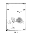
- Figure 10 is a representation of the total electronic charge density for the state associated with the DX- center for Si doped GaAs with the broken Si-As bond indicated as a dashed line.
- Figure 11 is a representation of the total electronic charge density associated with the lowest empty state associated with the DX- center for Si doped GaAs with the broken Si-As bond indicated as a dashed line.
- It has been traditionally believed that the DX center is a defect associated with all donors in AIGaAs and other III-V alloys. This idea has become widespread and has had experimental support whenever donor type dopants from Group IV and Group VI dopants, have been used in GaAs or AlxGa1-xAs alloys. The implicit assumption has been that the DX center will always appear in these n-type doped samples. The studies and work of the present inventor indicate that the DX center is associated with a substitutional type of donor per se and not with nonsubstitutional or interstitial donors. In this connection, reference is made to Part II herein which consists of a physical and mathematical analysis of the the origin of the DX center via structured models comprising Si and S induced DX centers in GaAs and includes an examination also of the energetics of DX formation and its electronic structure. The results were also extended to AlxGa1-xAs alloys via a simple theoretical model which is found to lead to results in impressive agreement with experiment for the binding energy of the DX center as a function of alloying. The conclusions reached from this analysis are that: (i) The DX center is a highly localized and negatively charged center resulting from the reaction, 2do - d + DX-, where dO and d+ represent neutral and ionized fourfold coordinated substitutional donors from the Group IV and Vi elements. The donors dO need not be spatially close to each other. What this translates to is that in the case of two substitutional donor atoms one atom loses an electron (e.g., d = Si ) and another atom gains the electron (e.g., DX = Si ). (ii) This defect formation involves a large bond-rupturing displacement of either the donor atom itself, as in for the case of a Group IV dopant such as Si, or one of its nearest-neighbor Ga (or Al) atoms, as in for the case of a group VI dopant such as S, along a bond axis.
- The above results, supported by the calculations and analysis in Part II, demonstrate that the formation of a DX center and the concomitant shallow-deep transition of the donor level in n-GaAs or n-AlxGA1-xAs is accompanied by a bond breaking distortion at a substitutional donor site in the lattice structure. Thus, can the creation of DX centers be inhibited through the use of donor atoms which give rise to shallow levels but, on the other hand, are not susceptible to this type of lattice instability? The foregoing analysis leads to the indication that the conventional doping procedure which relies on the introduction of substitutional donor atoms from Group IV or Group VI of the Periodic Table into the lattice should be modified or even abandoned since these atoms are a direct consequence of the DX center formation. This particular fact has not been known or appreciated by physicists and those skilled in the art as they have consistently attempted to rid the lattice of III-V semiconductors of the DX center by Group IV and Group VI doping followed by some other treatment or process to determine whether the effect of the DX center is alleviated. Group IV or VI atoms sit primarily at substitutional sites in the lattice and susceptible to a very large lattice relaxation which will always drive their shallow donor levels into deep donor levels. The bond breaking and lattice relaxation would not result if the doping were carried out interstitially rather than substitutionally. That is, if the atoms are introduced interstitially, i.e., between the other lattice atoms in the crystal, and not substitutionally for crystal atoms, there is an avoidance or significant suppression of the formation of the DX center or deep donor levels. This is because these interstitial atoms do not undergo the same lattice distortions as substitutional atoms and have no energy or motivation to transfer to a deep level, i.e., they are structurally stable. Interstitially they are shallow donors and remain shallow donors.
- There are several types of impurities that are possible for interstitial doping and the simplest form for interstitial donors would be Group V and Group III atoms. It is widely believed by those skilled in the art that group III dopants will create acceptors but as supported by the calculations in Part II, interstitial incorporation of Group III atoms will behave as a donor and not an acceptor.
- Interstitial Group V dopants, preferably As and Sb, and possibly P and N, are particularly suitable since these dopants are always donors, whether incorporated interstitially or substitutionally into the lattice. A Group V dopant incorporated substitutionally on the wrong lattice site still functions as a donor. An example is As occupying a Ga site (called an As antisite), which is also known as an EL2 center. See, D.J. Chadi et al. "Metastability of the Isolated Arsenic-Antisite Defect in GaAs", Physical Review Letters, Vol. 60, pp. 2187-2190, 1988.
- Interstitial Group III dopants, preferably Ga Al, and B, are also suitable. Interstitial Group III dopants have three valence electrons two of which are in low energy s-states and would lie below the valence band in AlxGa1-xAs alloys and are electronically inactive. The remaining p-electron has an energy that, in the limit of weak interactions with neighboring atoms, falls very near or above the conduction band, for B, Ga and Al. The Group III atoms, particularly Ga and Al, may be ideally suited for doping when introduced into interstitial sites. A potential problem, however, in introducing these Group III atoms into the lattice is the possibility of forming substitutional cation antisites which will behave as double acceptors thereby compensating the donor electrons arising from the interstitially introduced atoms. This problem is reduced to acceptable levels if Group III atoms are maximized for interstitial incorporation rather than substitutional incorporation in the lattice. In particular, Ga antisites will be statistically balanced by other donor type defects when Ga is introduced via ion implantation For example, the creation of an As-interstitial, As-vacancy pair will lead to n-type behavior since the As interstitial and As vacancy defects are individually donor type defects. Without this balance and in the presence of too many antisites, the incorporation of Group III atoms at substitutonal sites will result in double acceptor formations which will lead to a neutralization of two donor electrons of two interstitial site electrons. In this case there will be a low supply of electrons to provide for suitable and practical device operation. A specific example B is incorporated in GaAs wherein, besides being incorporated interstitially, it may also incorporate on a Ga site, which results in an isovalent impurity. However, B on a As site provides a double acceptor and effectively neutralizes two donor electrons at separate interstitial As sites in the lattice.
- Calculations on As antisite defects interacting with an As interstitial (See: G.A. Baraff et al., "EL2 and the Electronic Structure of the ASGa-As1 Pair in GaAs: The Role of Jahn-Teller Relaxation", Materials Research Society Symposium Proceedings, Vol. 104, edited by M. Stavola, S.J. Pearton, and G. Davies, Materials Research Society, Pittsburgh, Pennsylvania, pp. 375-386, 1988), suggest that an isolated interstitial As atom has an electronic level which-lies above the conduction band in GaAs and which, therefore, empties its electron into the conduction band. This electronic level structure provides an explanation as to why the isolated As interstitial, if present in GaAs, has not been detected via electron-spin-resonance experiments. The presence of As interstitials provides a plausible explanation for the large enhancement in the room temperature free carrier density in a limited AI concentration range observed by Basmaji et al., supra, in AlxGa1-xAs alloys grown by metalorganic vapor phase epitaxy (MOVPE) under a high As/(Ga + Al) ratio of 95 and at a high growth temperature of 950 ° C. The samples in the Basmaji et al. experiment were doped with Sn in Group IV during growth. As explained in more detail later, experiments herein were conducted which clearly demonstrate the detrimental effects of Group IV dopants and which provide clear indication for the feasibility and utility of interstitial doping.
- With respect to Group V dopants, As is an excellent choice in the case of high electron mobility transistors (HEMT). The reason is that the incorporation of As as a dopant has three possible choices of incorporation: (1) As substituted at an As site, which is fine; (2) As substituted at an Ga site, which is a deep donor and not desirable but fine, and, (3) As incorporated interstitially in the lattice behaving as a shallow donor, which is preferred. Thus, all three possibilities for As are good because As substitutionally on its own site or interstitially are fine and the substitution at Ga sites forming As antisites gives rise to a deep donor and not a deep acceptor. The deep donor is also referred to as an EL2 center in GaAs and as a deep donor, it does not interfere with the n-type doping resulting from interstitial As atoms. Deep acceptors, if present to an appreciable extent, would compensate shallow donors provided by interstitial As sites and render the material useless. The density of shallow donor electrons close to the conduction band provided by interstitial As sites is quite adequate for HEMT applications.
- There are many other possible candidates for n-type interstitial doping of III-V alloys. Lithium, for example, should lead to a shallow donor state, however, its mobility may be too high and it may gradually diffuse out of the sample. Calcium is another possibility and it should also lead to shallow donor states. Another possible candidate for an interstitial donor is Cu. It is known that Cu goes into GaAs interstitially and gives a shallow donor level. The problem with Cu appears to be that it tends to form defect complexes and its suitability for doping of high or moderate AI content AlxGa1-xAs alloys requires further examination.
- Other examples of III-V semiconductors acceptable for interstitial doping as taught herein include GaAsP, GaAsSb and AIGaAsP, AIGaSb and GalnAsP alloys.
- The introduction of Group III or Group V dopants in III-V semiconductors may be accomplished by several methods, such as high overpressure of the group III or Group V dopant in its gaseous form during MOVPE or MBE growth of the III-V semiconductor, ion implantation after crystal growth, and excess group V (or III) atoms in the melt during crystal growth.
- The following are experimental examples of interstitial doping in III-V semiconductors. These particular examples are given only for the purpose of illustrating a method of introducing interstitial doping that may be employed and are not intended to imply a preference for any particular form of incorporation or usage of a particular interstitial dopant because each particular III-V semiconductor and chosen interstitial dopant will require initial determination of parameters for the chosen method, such as growth temperature, overpressure, gas constituent ratios, ion implant energy, substrate temperature, etc.
- As shown in Figures 1, 3 and 5, three
different samples overlayer layer GaAs substrate layers sample 10 of Figure 1,underlayer 14 contain approximately 22% AI whileoverlayer 16 contained approximately 31% Al. Insample 20 of Figure 3,underlayer 24 contain approximately 24% AI whileoverlayer 26 contained no Al, i.e., was deposited as GaAs. Insample 30 of Figure 5,underlayer 34 contain approximately 21% AI whileoverlayer 36 contained approximately 52% Al. Thus, insamples - Free electron concentrations on both the AlxGa1.xAs layers 16, 26 and 36 and AlyGai.yAs layers 14, 24, and 34 were determined as a function of sample depth and a SIMS analysis was done to test any possible correlation of the free electron density with the concentration of Si impurities which were intentionally introduced during the growth phase. The results for each of the three
samples - For all three
samples AI containing layers - For
sample 20 in Figure 3, for example, the free carrier concentration inregion 26 is nearly equal to the Si concentration. Since the AI concentration is zero in this region, there should be no deep trap states and the prediction that the free carrier concentrations should be equal to the Si plus the interstitial densities indicates that there are very few As interstitials in this sample. This leads to the prediction that the free carrier concentration inregion 26 where the AI concentration is 26 should be very small because there are few As interstitials and because all the donor electrons from Si will be trapped on DX centers. The experiments verify this prediction and show a large drop in the free carrier density inregion 26. - For
sample 30 in Figure 5, the free carrier density is approximately 1017 cm-3 inregion 36 where the Al concentration is high. This is about one third of the Si density. Inregion 36, however, the carrier density is significantly larger than the Si density because of the presence of As interstitials. The As interstitial density is predicated to be larger by at least 1017 cm-3 than the Si concentration inregion 36, to give the observed free carrier density. This implies that the As interstitial density in region 36 (and, therefore, region 34) is about 3-4x 10¹⁷. Inregion 36 where the Si concentration is very low, the carrier density is nevertheless quite high. The theory predicts that the carrier density in this region should be equal to the As interstitial density inregion 36 which is assumed to be the same as inregion 34 plus the Si density inregion 34. The experimental result confirm this prediction. - The data for all three
samples AI containing regions - The following scientific, theoretical and physical analysis is offered as additional support for the present invention. The experimental data set forth previously for the three samples in Part I supports the conclusions reached in this analysis.
- The following is a more detailed discussion of the results of the theoretical study of the atomic and electronic structure of DX centers in GaAs and AIGaAs alloys. The approach to the problem of the DX center is presented in two complementary ways. In Section A, a simple expression for the composition and pressure dependence of the binding energy of DX centers in AIGaAs alloys is proposed. The major conclusion drawn from this analysis is that the much discussed correlation between the DX and L conduction-band-minimum energies can be satisfactorily explained without the assumption that DX is an L-derived effective-mass like level.
- In Section B the structural, energetic, and electronic aspects of Si and S induced DX centers in GaAs is addressed using an ab initio self-consistent pseudopotential approach. The results of these calculations indicate that DX is a strongly localized and negatively charged defect which behaves as a negative-U center. The calculated atomic structure for DX is shown to be characterized by a very large dopant- dependant lattice relaxation. In addition, the large Stokes shift between the thermal and optical binding energies, and the barriers for electron capture and emission are shown to be properly accounted for by the predicted structural models for Si and S induced DX centers.
- The results of the previous two sections are used in Section C to suggest that: The formation of DX centers is associated with structural transformations which are specific to substitutional donors and unlikely to occur for interstitial donors. The experimental results on a reduction in DX concentration in the samples reported in Part I, achieved through the preparation technique of As overpressure is concluded to be caused by an unanticipated formation of a large nubmer of interstitial donors. The advantages and disadvantages of using particular interstitial dopants are examined. A summary of the main results of this analysis is given in Section D.
- In the nondegenerate doping limit, the DX center is proposed to result from the following set of reactions:


- In Eqs. (1 )-(3)drepresents a normal fourfold coordinated substitutional donor, DX denotes the broken bond configurations shown in Figures 7A and 7B, e denotes a free electron in the conduction band, and the superscripts specify the charge states. The neutral donors in Eq. (3) are not necessarily in close spatial proximity of each other to form DX-. Equation (3) indicates that the density of DX centers should, at most, equal one half the density of the donor atoms. This will hold if there is no other shallow donor which is itself stable against a DX-like transformation but which can act as a reservoir to supply the free electrons needed to drive the donors in Eq. (3) into the DX state. As discussed in Section B, the energies of both the DX° and DX+ states are found to be significantly larger than those of cP and d+ and there is no energy barrier for the transformations between the structures. This is the reason why the reaction in Eq. (3) is not written in the form 2DX° → DX+ + DX-.
- In highly doped samples where the electrons form a degenerate gas and the donors are nearly all ionized, DX formation may occur from the capture of two electrons by an ion: d+ + 2e → DX• (4)
- The atomic distortions responsible for the formation of DX involve a large lattice displacement which leads to the breaking of a donor-lattice bond. The notation DX is used e to refer to the broken-bond configurations disclosed in Figures 8A-8D. The consequences of Eqs. (l)-(4) for the properties of DX centers are analyzed in the following sections. The dependence of the binding energy of DX centers on alloy composition, pressure, and dopant concentration as a function of its charge state is examined below.
- A more detailed examination of the simple expression for the thermal binding energy Eo of DX centers will now be considered, having been recently suggested in Chadi et al , Physical Review Letters, Vol. 61, p. 873 et seq., August, 1988. For a neutral center the binding energy E0(Dx°) relative to the conduction band minimum (CBM) in AlxGa xAs alloys was proposed to vary with alloying as

ΔE DX0, relative to the VBM is given by
- In writing Eq. (6) we are implicitly assuming that the impurity potential is not strong enough to cause a mixing of the higher lying conduction bands. Exceptions to Eq. (6) can arise when the difference between the potentials of the host and impurity atoms is sufficiently large to cause an appreciable mixing of other conduction (or possibly valence) bands. The symmetry of the deep center may also play an important role in determining the actual mix of the conduction band states.
- The assumption that DX is derived from all the states of the lowest conduction band implies:


- The energy of the neutral DX center for the particular choice of wave function made in Eq. (7) is given by:

- The BZ average of the conduction band energy needed to determine ΔECB in Eq. (6) can be carried out in a number of ways. The most direct method is to use a fine mesh of points in reciprocal space for the averaging. A much simpler approach is to use the "special points" approach which relies on a few well chosen representative points. The hierarchy of the special point sets for fcc Bravais lattices appropriate for GaAs and AIGaAs alloys has been previously determined. The desired average can be determined with high accuracy as the number of special points used in the sampling is increased. A zeroth order approximation to the average energy is ΔECBΔE(L). A more accurate approximation, which is discussed in the Appendix, is obtained by using the energies at the r, X, and L points according to the prescription


- The variation with alloying of the BZ averaged energy of the lowest conduction band obtained from Eqs. (10)-(13) is given by

- The three point r, X, L averaging gives a variation of EcB with x which is only 86% of the rate of the corresponding change of E(L) instead of being equal to it when the zeroth order approximation ΔECB = ΔE-(L) is used.
- Equations (11)-(13) show that the CBM is at r for x≦0.46 and at the X point of the BZ for x>0.46. Equations (5)-(14) therefore predict:

- For a negatively charged center arising from Eq. (3) we need the variation of the energy of DX- + d relative to 2d°. Using the same approach as above, this difference is equal to: ΔE0(DX-) = 2A(EcBM-EcB) =

- For a neutral center the densities of d0 and DX0 are related by


- The ratio ndol nDX determined from Eqs. (18) and (20) is independent, therefore, of the charge state of DX The experimentally derived binding energies13 which are based on a βΔE0 dependence in the Boltzmann factor need to be multiplied by two for a negatively charged state. In the following, in order to compare the predictions of the simple model with the experimental data of Chand et al., Physical Review B, Vol. 30, p. 4481 et seq., 1984, the expressions for AEo(DX°) given by Eqs. (15) and (16) are used. The factor of two difference between ΔE0(D)0)ΔE0(DX-) state should be borne in mind, however.
- Equations (15)-(16) show that the binding energy of DX relative to the CBM increases with AI concentration until the direct-indirect band gap transition at x=46% and then it decreases. The predicted extremum of x=46% for the DX binding energy is in good agreement with the experimentally determined range of 0.45≦X≦0.48. The 0.7 eV prefactor in Eqs. (15) for x<0.46 is nearly identical with the 707 meV value obtained by Chand et al. from a best fit to their data. The variation above x=0.46 is also in very good agreement with experimental data.
- Equations (6), (13), and (14) show that the thermal occupancy level EDx relative to the VBM varies as if it is tied to the L point of the conduction band. The correlation between the motion of the two, as measured by the ratio of the coefficients of Ax in Eqs. (13) and (14), is 0.55/0.64=86%. This is very nearly the same as the measured correlation coefficient of 0.54/0.64=84%. The derivation of this result makes it clear, however, that: The L-like variation of the DX energy can be explained without the assumption that it is an L-derived effective mass level. The correlation between EDX and E(L) appears because ΔEDX≃ΔECB and ΔECB =AE(L). IF DX were an L-derived effective mass level, then ΔEDX would have to be exactly, and not merely approximately, equal to AE(L). Such an exact relationship between the DX and E(L) energy levels has not been experimentally established. In addition, an L-derived level, even when inter-valley scattering is accounted for, is a much more delocalized defect than is experimentally observed to be the case for DX. Since the special points derived relation ΔECB≈ΔE(L) is material independent, the correlation ΔEDX≈ΔE(L) is not restricted to AIGaAs alloys but should hold approximately in other materials.
- Other expressions for the alloy dependence of the band energies have been discussed by T. N. Theis, in Proceedings of the Third International Conference on Shallow Impurities in Semiconductors, August 10-12, 1988, Link6ping, Sweden (in press) and D. E. Aspnes, in Gallium Arsenide, Edited by J. S. Blakemore, American Institute of Physics No. 1, pp. 231-243, 1987. For the new parametrization schemes one also finds that the use of ΔEDX≈ΔECB together with the three point averaging scheme of Eq. (10), results in ΔEDX≃0.84ΔEL or ΔEDX≃0.77ΔE(L). This shows that EDX, for all reasonable parametrizations, most strongly correlated with E(L).
- The r, X, and L averaging scheme can also be used to determine the temperature dependence of the DX binding energy since the shifts of the energies of the band edge states with temperature are well known, particularly for GaAs. The temperature shifts of the r, X, and L conduction states with respect to the VBM have the same sign and are nearly equal to each other in GaAs. This implies that Eo(DXD) in GaAs should be approximately temperature independent.
- Making use of the experimental result that at x=0.22 the thermal binding energy of DX becomes equal to that of shallow donors (=6 meV), the inteqration of Eqs. (15) and (17) gives (in eV):


- The required 0.15-0.17 eV increase in [E(Γ)-ECB] needed to stabilize the DX center in GaAs translates to a pressure of 18-20 kbar. This result is consistent with experimental data, for example, see M. Mizuta et al., supra, which show the appearance of DX centers in GaAs at pressures of about 20-30 kbars. In the direct gap region, the calculated pressure coefficient ΔE0(DX) ΔP of 8.4 meV/kbar is consistent with the experimentally determined values from pressure and temperature dependent Hall measurements in GaAs and Alo.15 Gao.85 As and with other recent measurements which give values in the range of 6 to 7.5 meV/kbar. In the indirect gap regime the pressure coefficient ΔE0(DX) i AP is calculated to be -5.2 meV/kbar. The change in sign of the pressure coefficient and its magnitude are also consistent with recent experimental results.
- If DXwere a neutral center resulting from the reaction


- The energy of the DX resonance above the CBM is experimentally observed to increase slightly with dopant density in the high doping regime in GaAs. A very small increase (= 1 meV) in the DX energy is expected from Eq. (7) when the sum over the conduction band states is restricted to be over only the unoccupied states. This is due to the fact that even at the highest doping levels,9.10 e.g., n = 18x1019 cm-3, the volume of k-space occupied by the free electrons is extremely small. The shifting of EDX with respect to the CBM is mainly due to band gap renormalization in heavily doped semiconductors resulting from the Coulombic interactions between the electrons. One effect of this renormalization is a lowering of the energies of the states near the Γ1 conduction band which will show up as an effective increase in the position of the DX level with respect to the CBM. The approximate size of the reduction in the energy of the Γ1 state is given by


- A brief description of ab initio self-consistent calculations for Si and S substitutional donors in GaAs is set forth in Chadi et al., supra, in Section A2. The calculations for the d0, d, DX0, DX+, and DX- structural states were each done separately using an 18 atom √3×√3×√6 hexagonal supercell with its c-axis oriented along the [111] axis. The unit cell although relatively small is still sufficiently large to provide reliable information on the structural properties of DX centers. The same unit cell was used in our previous study of the E12 defect center in GaAs. The results obtained in that case for the charge density distributions and structural properties of the antisite were found to be in good accord with a similar calculation employing a 54 atom cell. For the present study, the band dispersion of the donor state from the zone center to the Brillouin zone edge, resulting from the use of a finite sized cell, is calculated to be 0.2 eV. The local phonon vibration mode for the Si on Ga-site donor is calculated to be nearly 334 cm-1 as compared to the experimental values of 379-384 cm-1. Our calculations indicate that the mode is quite anharmonic.
- The optimal atomic coordinates were determined by minimizing the total-energy. Hellmann-Feynman forces were calculated and utilized in the optimization process. Our calculations show that a neutral donor is stable against Jahn-Teller distortions in GaAs. The major result of our calculations is, however, that a metastable state with a large lattice relaxation leading to a broken bond configuration (Fig. 2) and a C3v symmetry, is possible for a negatively charged center. As discussed below, this center has many of the properties associated with the DX center. For a Si donor, the distortion leading to DX formation involves a 1.17 A motion of the Si atom away from one of its nearest neighbor As atoms, along the bond axis, into a threefold coordinated interstitial position. The bonding configuration for the Si atom changes from Sp3 to Sp2 as a result of the relaxation. This is best seen by the 118.4 angles about the Si atom in the interstitial configuration. The threefold coordinated As atom resulting from the Si displacement relaxes outward, reducing its angles from 109 47 to 106.5 Electronic charge is transferred from the Si atom to the As atom in this process. Maximal bond-length changes of -2.4% between Ga and As atoms near the Si donor are found. For a S donor one of the nearest-neighbor Ga (or Al) atoms of the S dopant moves by 1.13 A into an interstitial position. A sulfur-gallium bond is broken as a result of this relaxation. The bond angles about the threefold coordinated Ga (or AI) atom are calculated to be 118.3* and those around S about 112°. Maximal bond-length changes of +2.8% between Ga and As atoms are found for this case. The valence electron charge density for a Si induced DX- center is shown in Figure 9. The atomic distortions in Figure 10 are nearly identical to those predicted to occur in the metastable state of the EL2 related AsGa antisite defect in GaAs.
- The reaction represented by Eq. (3) is calculated to be energetically unfavorable by 0.22±0.1 eV for both Si and S donors in GaAs. The surprisingly small value of the total-energy differences and the near equivalence of the results for Si and S are in qualitative agreement with the =0.3 eV estimate from Eq. (21). When the charge of the DX- center is changed to DX0 or DX the interstitial atomic configuration is found to be highly unstable with respect to the ordinary fourfold coordinated substitutional geometry and there is no barrier for the transformations to this geometry. The DX0 to d0 transition is calculated to be exothermic by = 1.3 eV.
- The threefold symmetric C3v structure proposed for the DX center is in agreement with the experimentally derived symmetry from phonon transmission measurements. These experiments show a trigonal symmetry for Sn-doped samples and an orthorhombic or trigonal symmetry for Te doped ones. Other experiments based on analyses of extended X-ray absorption fine structure (EXAFS) have also provided information on the local atomic environment of DX centers. The EXAFS results of Sette et al., Physical Review Letters, Vol. 56, p. 2637 et seq., 1986, for S-doped GaAs show that there are two types of atomic environments around the S atoms. One-half the S atoms are found to be in their normal subtitutional positions but the local environment of the other half is found to be severely distorted. This picture is in good agreement with predictions for S-induced DX centers. However, Mizuta et al., Applied Physics Letters, Vol. 52 p. 126 et seq., 1987, using the same technique infer a very small lattice relaxation for the case of Se. More recently Mossbauer spectroscopy has been applied to Sn doped samples and the results seem to indicate a significant local distortion of atoms around Sn.
- Calculations show that although the Si and S induced DX centers in GaAs are metastable, they have optically deep electronic levels associated with them The optical ionization energies are calculated to be 1.05 eV for GaAs:Si and 0.74 eV for GaAs:S. The optical ionization energies are predicted to increase with pressure or alloying in AlxGa1-xAs. In the composition range where the band gap is direct (i.e., x≦0.46) the optical gap is expected to vary as

- The results of the pseudopotential calculations provide further insight into how the shallow-deep transition depicted by Eq. (3) takes place. The calculations show that when a neutral Si donor atom is displaced away from its nearest-neighbor along a bond axis, the total-energy increases as expected but the donor level becomes increasingly deeper as the displacement becomes larger. When the level has dropped by more than the on-site Coulomb repulsive term U, which is calculated to be =0.20-0.22 eV, the d° level can capture a free electron without expelling it immediately back into the CBM. At this point the formation of a d- center leads to a further motion of the Si atom which transforms it into a DX- center. The energy barrier for electron capture Ecap in lightly-doped GaAs is calculated to be 0.55±0.05 eV corresponding to the rise in energy for a 0.5 A displacement of the Si atom. Combining this with the result of the total-energy calculation which shows that DX is unstable by =0.22 eV with respect to shallow donors in GaAs, the emission barrier is estimated to be 0.33±0.1 eV.
- The results of the ab initio pseudopotential calculations discussed in the previous Section B show that the formation of a DX center and the concomitant shallow-deep transition of the donor level in n-type GaAs is accompanied by a bond-breaking distortion at a substitutional donor site. The question naturally arises, therefore, whether the creation of DX centers can be inhibited through the use of donor atoms which give rise to shallow levels but which are not susceptible to the same type of lattice instability. The possibility of replacing substitutional donors with interstitial ones which do not form strong bonds with their surrounding atoms may be considered. This indicates that the conventional doping procedure which relies on the introduction of atoms from column IV or VI of the Periodic Table into the lattice needs to be modified or possible abandoned. There are many possible choices for interstitial doping of AIGaAs alloys. The simplest choices are probably from group III and V atoms. In the following, the merits of each choice is examined.
- Recent calculations of Baraff et al., Physical Review B, Vol. 38, p. 6003 et seq., 1988 and Physical Review B, Vol. 35, p. 6154 et seq., 1987, suggest that an interstitial As atom has an electronic level which lies above the CBM in GaAs and which, therefore, empties its electron into the conduction band. This electronic level structure provides an explanation for why the isolated As interstitial, if present in GaAs, has not been detected via electron-spin-resonance experiments. Optically detected electron-nuclear double resonance experiments provide, however, strong evidence for the presence of As interstitials in GaAs samples grown in an As rich environment. The presence of As interstitials would provide a simple explanation for the large enhancement in the room temperature free carrier density observed by Basmaji et al., supra, in AIGaAs alloys grown by metalorganic vapor phase epitaxy under a very high As / (Ga + Al) ratio of 95. The samples in this experiment were doped with Sn which, according to theory, will actually tend to reduce the free electron concentration arising from the As interstitial atoms because of its tendency to form DX centers in high AI content alloys. As indicated in connection with the three samples in Part I, the experimental results indicate that donors not susceptible to DX like instabilities, which arise from As interstitials, can be introduced into AIGaAs alloys with a high AI content with densities of about 2-3x1017 cm 3. In these samples the free carrier density is observed to decrease with increasing Si impurity content in AIGaAs alloys with high AI densities and to increase with it when the AI content is low.
- The use of a high As flux during growth can lead to the formation of As antisites in addition to As interstitials. The As antisite defect is known to be a (deep) donor so it should not interfere with the n-type doping resulting from interstitial arsenic atoms.
- Interstitial group III dopants have three valence electrons two of which are in low energy s-states and would lie below the VBM in AIGaAs alloys and the other is a p-electron with an energy that, in the limit of weak interactions with neighboring atoms, should fall several eV above the CBM, for Ga and AI and near the CBM of GaAs for B. An interstitial atom is, in general, strongly interacting with its neighbours. The ab initio self-consistent calculations of Baraff et al., Physical Review Letters, Vol. 55, p. 1327 et seq., 1985, demonstrate, however, that Interstitial Ga does, in fact, behave as a donor and not an acceptor in GaAs. These group III atoms, particularly Ga and Al, would be, therefore, ideally suited for n-type doping if they can be in some manner introduced into interstitial sites. A potential problem with trying to incorporate these atoms into the lattice via ion implantation is the possibility of forming substitutional cation antisites which will behave as double acceptors in n-type materials thereby compensating the donor electrons arising from the interstitial atoms. However, Ga antisites should be statistically balanced by other donor type defects. For example, the creation of an As-interstitial, As-vacancy pair will lead to n-type behavior since the As interstitial and As vacancy defects are individually donor type defects. A Ga vacancy defect would be an acceptor and it would have a high probability of annealing out as a result of recombination with either Ga or As interstitial atoms. The formation of energies for these defects is very sensitive to Ep with acceptor-like defects becoming energetically more favorable in n-type samples and vice versa. Despite the potential complications of introducing interstitial donors, and the question of the stability of these donors, the possibilities for this type of doping procedure are very important and deserve more critical experimental investigations.
- The only group III atom which has been examines so far for its effect on DX centers is boron. The experiments of Li et al., supra, show that incorporation of B in Si-doped GaAs leads to two new donor levels with reduced emisssion and capture activation energies (compared to DX centers). The experiments were carried out at pressures of 20-30 kbars where DX is ordinarily more stable than shallow donors. A similar effect has not yet been found in an AIGaAs alloy. The fact that the DX centers are observed to go away with the introduction of B could be indicative of B-Si complex formation which prevents the Si atom from going into the threefold coordinated interstitial position necessary for DXformation. Since the concentration of the B impurities in the samples studied was at least twice that of Si, the possibility of interstitial B atoms which are not interacting with any Si atoms cannot be discounted. A different possible explanation is discussed below.
- The inventor has done self-consistent pseudo-potential calculations on interstitial B in pure GaAs and has tested two different interstitial positions for which the nearest neighbours of B are either all Ga (Tdi) or all As atoms (Td2). The inventor has found that for the relaxed structures the most stable site for B, in either neutral or negative charge states, is at the Td2 site whereas for a positive charge state it is at the T d1 site. The energy differences between the two sites are nearly 0.22 eV for B°, 0.4 eV for B-, and 0.2 eV for B~. combining the results of the calculations for B with those for Si it is found that the reaction


- In conclusion, experimental data on the composition, pressure, and dopant concentration dependence of the DX binding energy in AlxGa1.xAs alloys were analyzed using a simple theoretical model. The results of ab initio pseudopotential calculations indicate that DX is a negatively charged and highly localized defect center resulting from a large lattice distortion leading to bond rupture at the donor site. The analysis and discussion concludes that DX centers are associated with substitutional donors only and that it is possible to reduce their concentration by introducing interstitial dopants which do not undergo the same type of large lattice relaxations responsible for deep electron trap formation. The possibilities of using group III or V elements for this purpose are examined and confirmed by experiment.
Claims (10)
Applications Claiming Priority (2)
| Application Number | Priority Date | Filing Date | Title |
|---|---|---|---|
| US27682488A | 1988-11-28 | 1988-11-28 | |
| US276824 | 1988-11-28 |
Publications (3)
| Publication Number | Publication Date |
|---|---|
| EP0371684A2 true EP0371684A2 (en) | 1990-06-06 |
| EP0371684A3 EP0371684A3 (en) | 1991-01-23 |
| EP0371684B1 EP0371684B1 (en) | 1996-03-13 |
Family
ID=23058208
Family Applications (1)
| Application Number | Title | Priority Date | Filing Date |
|---|---|---|---|
| EP89312111A Expired - Lifetime EP0371684B1 (en) | 1988-11-28 | 1989-11-22 | Interstitial doping in III-V semiconductors to avoid or suppress DX centre formation |
Country Status (3)
| Country | Link |
|---|---|
| EP (1) | EP0371684B1 (en) |
| JP (1) | JPH02188932A (en) |
| DE (1) | DE68925944T2 (en) |
Cited By (1)
| Publication number | Priority date | Publication date | Assignee | Title |
|---|---|---|---|---|
| US11305664B2 (en) * | 2017-10-17 | 2022-04-19 | Easelink Gmbh | Ground contact unit for a vehicle battery charging system and method for switching a contact area of a ground contact unit |
-
1989
- 1989-11-21 JP JP1303043A patent/JPH02188932A/en active Pending
- 1989-11-22 DE DE68925944T patent/DE68925944T2/en not_active Expired - Fee Related
- 1989-11-22 EP EP89312111A patent/EP0371684B1/en not_active Expired - Lifetime
Non-Patent Citations (5)
| Title |
|---|
| APPLIED PHYSICS LETTERS, vol. 53, no. 26, 26th December 1988, pages 2653-2655; M.K. LEE et al.: "Isoelectronic doping in GaAs epilayers grown by molecular beam epitaxy" * |
| JOURNAL OF VACUUM SCIENCE & TECHNOLOGY B, vol. 4, no. 2, March/April 1986, pages 521-523; T.M. KERR et al.: "Summary abstract: State-of-the-art AlGaAs alloys by antimony doping" * |
| PHYSICA STATUS SOLIDI (a), vol. 100, pp. K41-K45 (1987) * |
| PHYSICAL REVIEW B, vol. 39, no. 14, 15th may 1989, pages 10063-10074; D.J. CHADI et al.: "Energetics of DX-center formation in GaAs and AlxGa1-xas alloys" * |
| PHYSICAL REVIEW LETTERS, vol. 55, 1985, pages 1327-1330; G.A. BARAFF et al.: "Electronic structure, total energies, and abundances of the elementary point defect in GaAs" * |
Cited By (1)
| Publication number | Priority date | Publication date | Assignee | Title |
|---|---|---|---|---|
| US11305664B2 (en) * | 2017-10-17 | 2022-04-19 | Easelink Gmbh | Ground contact unit for a vehicle battery charging system and method for switching a contact area of a ground contact unit |
Also Published As
| Publication number | Publication date |
|---|---|
| EP0371684B1 (en) | 1996-03-13 |
| EP0371684A3 (en) | 1991-01-23 |
| DE68925944T2 (en) | 1996-11-14 |
| DE68925944D1 (en) | 1996-04-18 |
| JPH02188932A (en) | 1990-07-25 |
Similar Documents
| Publication | Publication Date | Title |
|---|---|---|
| Walukiewicz | Intrinsic limitations to the doping of wide-gap semiconductors | |
| Stampfl et al. | Native defects and impurities in InN: First-principles studies using the local-density approximation and self-interaction and relaxation-corrected pseudopotentials | |
| Laks et al. | Role of native defects in wide-band-gap semiconductors | |
| Shih et al. | Band gap reduction in InAsN alloys | |
| Deppe et al. | Impurity diffusion and layer interdiffusion in Al x Ga1− x As‐GaAs heterostructures | |
| Wager | Energetics of self‐diffusion in GaAs | |
| Deppe et al. | Layer interdiffusion in Se‐doped AlxGa1− xAs‐GaAs superlattices | |
| Suski et al. | High pressure and DX centers in heavily doped bulk GaAs | |
| Bracht et al. | Enhanced and retarded Ga self-diffusion in Si and Be doped GaAs isotope heterostructures | |
| US5139960A (en) | Interstitital doping in III-V semiconductors to avoid or suppress DX center formation | |
| Uedono et al. | Electron capture by vacancy-type defects in carbon-doped GaN studied using monoenergetic positron beams | |
| EP0371684B1 (en) | Interstitial doping in III-V semiconductors to avoid or suppress DX centre formation | |
| Fujiwara et al. | Carrier transport properties of iodine‐doped (ZnS) 3 (ZnSe) 42 ordered alloys grown by atomic layer epitaxy | |
| Bonapasta et al. | Effects of strain and local charge on the formation of deep defects in III-V ternary alloys | |
| Barcz et al. | Channels of Cd diffusion and stoichiometry in CdTe grown by molecular beam epitaxy | |
| Wang et al. | On the physical origins of the EL2 center in GaAs | |
| Du | Defects in AlSb: A density functional study | |
| Bougrioua et al. | Mobility Collapse in Undoped and Si‐Doped GaN Grown by LP‐MOVPE | |
| Hamoudi et al. | Cation interdiffusion in InGaAsP/InGaAsP multiple quantum wells with constant P/As ratio | |
| Gherasoiu et al. | Mg induced compositional change in InGaN alloys | |
| Chisholm et al. | The electrical activity of GaN doped with transition metal impurities | |
| Cheng et al. | Compound Semiconductor Crystals | |
| Nakagawa et al. | Anomalous mobility enhancement in Si doping superlattices | |
| Iguchi | Atomic diffusion mediated by intrinsic point defects in GaAs and AlxGa1− xAs–GaAs superlattices | |
| Laks et al. | Native Defect Compensation in Wide-Band-Gap Semiconductors |
Legal Events
| Date | Code | Title | Description |
|---|---|---|---|
| PUAI | Public reference made under article 153(3) epc to a published international application that has entered the european phase |
Free format text: ORIGINAL CODE: 0009012 |
|
| AK | Designated contracting states |
Kind code of ref document: A2 Designated state(s): DE FR GB |
|
| PUAL | Search report despatched |
Free format text: ORIGINAL CODE: 0009013 |
|
| AK | Designated contracting states |
Kind code of ref document: A3 Designated state(s): DE FR GB |
|
| 17P | Request for examination filed |
Effective date: 19910701 |
|
| 17Q | First examination report despatched |
Effective date: 19930630 |
|
| GRAA | (expected) grant |
Free format text: ORIGINAL CODE: 0009210 |
|
| AK | Designated contracting states |
Kind code of ref document: B1 Designated state(s): DE FR GB |
|
| REF | Corresponds to: |
Ref document number: 68925944 Country of ref document: DE Date of ref document: 19960418 |
|
| ET | Fr: translation filed | ||
| PGFP | Annual fee paid to national office [announced via postgrant information from national office to epo] |
Ref country code: FR Payment date: 19961111 Year of fee payment: 8 |
|
| PGFP | Annual fee paid to national office [announced via postgrant information from national office to epo] |
Ref country code: GB Payment date: 19961113 Year of fee payment: 8 |
|
| PGFP | Annual fee paid to national office [announced via postgrant information from national office to epo] |
Ref country code: DE Payment date: 19961202 Year of fee payment: 8 |
|
| PLBE | No opposition filed within time limit |
Free format text: ORIGINAL CODE: 0009261 |
|
| STAA | Information on the status of an ep patent application or granted ep patent |
Free format text: STATUS: NO OPPOSITION FILED WITHIN TIME LIMIT |
|
| 26N | No opposition filed | ||
| PG25 | Lapsed in a contracting state [announced via postgrant information from national office to epo] |
Ref country code: GB Free format text: LAPSE BECAUSE OF NON-PAYMENT OF DUE FEES Effective date: 19971122 |
|
| PG25 | Lapsed in a contracting state [announced via postgrant information from national office to epo] |
Ref country code: FR Free format text: THE PATENT HAS BEEN ANNULLED BY A DECISION OF A NATIONAL AUTHORITY Effective date: 19971130 |
|
| GBPC | Gb: european patent ceased through non-payment of renewal fee |
Effective date: 19971122 |
|
| PG25 | Lapsed in a contracting state [announced via postgrant information from national office to epo] |
Ref country code: DE Free format text: LAPSE BECAUSE OF NON-PAYMENT OF DUE FEES Effective date: 19980801 |
|
| REG | Reference to a national code |
Ref country code: FR Ref legal event code: ST |