EP0369574A2 - An improved method of fabricating solar cells - Google Patents
An improved method of fabricating solar cells Download PDFInfo
- Publication number
- EP0369574A2 EP0369574A2 EP89307405A EP89307405A EP0369574A2 EP 0369574 A2 EP0369574 A2 EP 0369574A2 EP 89307405 A EP89307405 A EP 89307405A EP 89307405 A EP89307405 A EP 89307405A EP 0369574 A2 EP0369574 A2 EP 0369574A2
- Authority
- EP
- European Patent Office
- Prior art keywords
- zone
- crystalline body
- hollow
- heater
- type conductivity
- Prior art date
- Legal status (The legal status is an assumption and is not a legal conclusion. Google has not performed a legal analysis and makes no representation as to the accuracy of the status listed.)
- Granted
Links
- 238000004519 manufacturing process Methods 0.000 title claims description 5
- 238000000034 method Methods 0.000 claims abstract description 50
- 239000002019 doping agent Substances 0.000 claims abstract description 36
- 239000000155 melt Substances 0.000 claims abstract description 18
- 239000007787 solid Substances 0.000 claims abstract description 13
- 239000000758 substrate Substances 0.000 claims abstract description 7
- 229910052710 silicon Inorganic materials 0.000 claims description 41
- 239000010703 silicon Substances 0.000 claims description 41
- XKRFYHLGVUSROY-UHFFFAOYSA-N Argon Chemical compound [Ar] XKRFYHLGVUSROY-UHFFFAOYSA-N 0.000 claims description 24
- 239000000463 material Substances 0.000 claims description 19
- 230000012010 growth Effects 0.000 claims description 18
- OKTJSMMVPCPJKN-UHFFFAOYSA-N Carbon Chemical compound [C] OKTJSMMVPCPJKN-UHFFFAOYSA-N 0.000 claims description 17
- 238000009792 diffusion process Methods 0.000 claims description 16
- 239000011248 coating agent Substances 0.000 claims description 13
- 238000000576 coating method Methods 0.000 claims description 13
- 229910052786 argon Inorganic materials 0.000 claims description 12
- 230000008569 process Effects 0.000 claims description 12
- PXHVJJICTQNCMI-UHFFFAOYSA-N Nickel Chemical compound [Ni] PXHVJJICTQNCMI-UHFFFAOYSA-N 0.000 claims description 10
- BHEPBYXIRTUNPN-UHFFFAOYSA-N hydridophosphorus(.) (triplet) Chemical compound [PH] BHEPBYXIRTUNPN-UHFFFAOYSA-N 0.000 claims description 10
- 239000004065 semiconductor Substances 0.000 claims description 9
- 239000007788 liquid Substances 0.000 claims description 6
- VYDNCCLNAHRIST-UHFFFAOYSA-N 13827-38-8 Chemical compound O1P(=O)(O2)O[Si]31OP2(=O)O3 VYDNCCLNAHRIST-UHFFFAOYSA-N 0.000 claims description 5
- 229910052759 nickel Inorganic materials 0.000 claims description 5
- ZOXJGFHDIHLPTG-UHFFFAOYSA-N Boron Chemical compound [B] ZOXJGFHDIHLPTG-UHFFFAOYSA-N 0.000 claims description 3
- 229910052782 aluminium Inorganic materials 0.000 claims description 3
- XAGFODPZIPBFFR-UHFFFAOYSA-N aluminium Chemical compound [Al] XAGFODPZIPBFFR-UHFFFAOYSA-N 0.000 claims description 3
- 229910052796 boron Inorganic materials 0.000 claims description 3
- 238000005520 cutting process Methods 0.000 claims description 3
- 239000011521 glass Substances 0.000 claims description 3
- 229910052698 phosphorus Inorganic materials 0.000 claims description 3
- HBMJWWWQQXIZIP-UHFFFAOYSA-N silicon carbide Chemical compound [Si+]#[C-] HBMJWWWQQXIZIP-UHFFFAOYSA-N 0.000 claims description 3
- 229910010271 silicon carbide Inorganic materials 0.000 claims description 3
- RYGMFSIKBFXOCR-UHFFFAOYSA-N Copper Chemical compound [Cu] RYGMFSIKBFXOCR-UHFFFAOYSA-N 0.000 claims description 2
- ATJFFYVFTNAWJD-UHFFFAOYSA-N Tin Chemical compound [Sn] ATJFFYVFTNAWJD-UHFFFAOYSA-N 0.000 claims description 2
- 230000001464 adherent effect Effects 0.000 claims description 2
- DHAHRLDIUIPTCJ-UHFFFAOYSA-K aluminium metaphosphate Chemical group [Al+3].[O-]P(=O)=O.[O-]P(=O)=O.[O-]P(=O)=O DHAHRLDIUIPTCJ-UHFFFAOYSA-K 0.000 claims description 2
- 229910052802 copper Inorganic materials 0.000 claims description 2
- 239000010949 copper Substances 0.000 claims description 2
- 238000005530 etching Methods 0.000 claims description 2
- 229910021397 glassy carbon Inorganic materials 0.000 claims description 2
- OAICVXFJPJFONN-UHFFFAOYSA-N Phosphorus Chemical compound [P] OAICVXFJPJFONN-UHFFFAOYSA-N 0.000 claims 1
- 239000011261 inert gas Substances 0.000 claims 1
- 239000011574 phosphorus Substances 0.000 claims 1
- 150000003018 phosphorus compounds Chemical group 0.000 claims 1
- 230000001681 protective effect Effects 0.000 claims 1
- XUIMIQQOPSSXEZ-UHFFFAOYSA-N Silicon Chemical compound [Si] XUIMIQQOPSSXEZ-UHFFFAOYSA-N 0.000 description 37
- 210000004027 cell Anatomy 0.000 description 27
- 239000007789 gas Substances 0.000 description 27
- 239000013078 crystal Substances 0.000 description 23
- 230000005855 radiation Effects 0.000 description 22
- 229910002804 graphite Inorganic materials 0.000 description 12
- 239000010439 graphite Substances 0.000 description 12
- 230000007246 mechanism Effects 0.000 description 7
- 238000002844 melting Methods 0.000 description 5
- 230000008018 melting Effects 0.000 description 5
- 238000009966 trimming Methods 0.000 description 5
- ZOKXTWBITQBERF-UHFFFAOYSA-N Molybdenum Chemical compound [Mo] ZOKXTWBITQBERF-UHFFFAOYSA-N 0.000 description 4
- 230000015572 biosynthetic process Effects 0.000 description 4
- 230000000694 effects Effects 0.000 description 4
- 239000012535 impurity Substances 0.000 description 4
- 229910052750 molybdenum Inorganic materials 0.000 description 4
- 239000011733 molybdenum Substances 0.000 description 4
- 230000009471 action Effects 0.000 description 3
- 229910052799 carbon Inorganic materials 0.000 description 3
- 238000010276 construction Methods 0.000 description 3
- 239000010408 film Substances 0.000 description 3
- 230000036433 growing body Effects 0.000 description 3
- 238000009413 insulation Methods 0.000 description 3
- XYFCBTPGUUZFHI-UHFFFAOYSA-N Phosphine Chemical compound P XYFCBTPGUUZFHI-UHFFFAOYSA-N 0.000 description 2
- QVGXLLKOCUKJST-UHFFFAOYSA-N atomic oxygen Chemical compound [O] QVGXLLKOCUKJST-UHFFFAOYSA-N 0.000 description 2
- 238000006243 chemical reaction Methods 0.000 description 2
- 238000002425 crystallisation Methods 0.000 description 2
- 230000008025 crystallization Effects 0.000 description 2
- 230000003247 decreasing effect Effects 0.000 description 2
- 238000010438 heat treatment Methods 0.000 description 2
- 238000001465 metallisation Methods 0.000 description 2
- 239000000203 mixture Substances 0.000 description 2
- 229910052757 nitrogen Inorganic materials 0.000 description 2
- 229910052760 oxygen Inorganic materials 0.000 description 2
- 239000001301 oxygen Substances 0.000 description 2
- 239000002904 solvent Substances 0.000 description 2
- 239000007858 starting material Substances 0.000 description 2
- 239000002699 waste material Substances 0.000 description 2
- 238000009736 wetting Methods 0.000 description 2
- NTIZESTWPVYFNL-UHFFFAOYSA-N Methyl isobutyl ketone Chemical compound CC(C)CC(C)=O NTIZESTWPVYFNL-UHFFFAOYSA-N 0.000 description 1
- UIHCLUNTQKBZGK-UHFFFAOYSA-N Methyl isobutyl ketone Natural products CCC(C)C(C)=O UIHCLUNTQKBZGK-UHFFFAOYSA-N 0.000 description 1
- GRYLNZFGIOXLOG-UHFFFAOYSA-N Nitric acid Chemical compound O[N+]([O-])=O GRYLNZFGIOXLOG-UHFFFAOYSA-N 0.000 description 1
- 229910052581 Si3N4 Inorganic materials 0.000 description 1
- XSTXAVWGXDQKEL-UHFFFAOYSA-N Trichloroethylene Chemical group ClC=C(Cl)Cl XSTXAVWGXDQKEL-UHFFFAOYSA-N 0.000 description 1
- PNEYBMLMFCGWSK-UHFFFAOYSA-N aluminium oxide Inorganic materials [O-2].[O-2].[O-2].[Al+3].[Al+3] PNEYBMLMFCGWSK-UHFFFAOYSA-N 0.000 description 1
- JNDMLEXHDPKVFC-UHFFFAOYSA-N aluminum;oxygen(2-);yttrium(3+) Chemical compound [O-2].[O-2].[O-2].[Al+3].[Y+3] JNDMLEXHDPKVFC-UHFFFAOYSA-N 0.000 description 1
- 238000013459 approach Methods 0.000 description 1
- 230000000712 assembly Effects 0.000 description 1
- 238000000429 assembly Methods 0.000 description 1
- JRPBQTZRNDNNOP-UHFFFAOYSA-N barium titanate Chemical compound [Ba+2].[Ba+2].[O-][Ti]([O-])([O-])[O-] JRPBQTZRNDNNOP-UHFFFAOYSA-N 0.000 description 1
- 229910002113 barium titanate Inorganic materials 0.000 description 1
- 239000000969 carrier Substances 0.000 description 1
- 238000001816 cooling Methods 0.000 description 1
- 230000008878 coupling Effects 0.000 description 1
- 238000010168 coupling process Methods 0.000 description 1
- 238000005859 coupling reaction Methods 0.000 description 1
- 230000007547 defect Effects 0.000 description 1
- 230000001419 dependent effect Effects 0.000 description 1
- 238000011161 development Methods 0.000 description 1
- 239000012153 distilled water Substances 0.000 description 1
- 230000005284 excitation Effects 0.000 description 1
- 230000004927 fusion Effects 0.000 description 1
- -1 i.e. Chemical compound 0.000 description 1
- 210000004692 intercellular junction Anatomy 0.000 description 1
- 238000003698 laser cutting Methods 0.000 description 1
- GQYHUHYESMUTHG-UHFFFAOYSA-N lithium niobate Chemical compound [Li+].[O-][Nb](=O)=O GQYHUHYESMUTHG-UHFFFAOYSA-N 0.000 description 1
- 230000005499 meniscus Effects 0.000 description 1
- 229910052751 metal Inorganic materials 0.000 description 1
- 239000002184 metal Substances 0.000 description 1
- 238000012986 modification Methods 0.000 description 1
- 230000004048 modification Effects 0.000 description 1
- 229910017604 nitric acid Inorganic materials 0.000 description 1
- NJPPVKZQTLUDBO-UHFFFAOYSA-N novaluron Chemical compound C1=C(Cl)C(OC(F)(F)C(OC(F)(F)F)F)=CC=C1NC(=O)NC(=O)C1=C(F)C=CC=C1F NJPPVKZQTLUDBO-UHFFFAOYSA-N 0.000 description 1
- 229910000073 phosphorus hydride Inorganic materials 0.000 description 1
- XHXFXVLFKHQFAL-UHFFFAOYSA-N phosphoryl trichloride Chemical compound ClP(Cl)(Cl)=O XHXFXVLFKHQFAL-UHFFFAOYSA-N 0.000 description 1
- 238000012545 processing Methods 0.000 description 1
- 238000010926 purge Methods 0.000 description 1
- 239000010453 quartz Substances 0.000 description 1
- VYPSYNLAJGMNEJ-UHFFFAOYSA-N silicon dioxide Inorganic materials O=[Si]=O VYPSYNLAJGMNEJ-UHFFFAOYSA-N 0.000 description 1
- HQVNEWCFYHHQES-UHFFFAOYSA-N silicon nitride Chemical compound N12[Si]34N5[Si]62N3[Si]51N64 HQVNEWCFYHHQES-UHFFFAOYSA-N 0.000 description 1
- 239000010409 thin film Substances 0.000 description 1
- 238000012546 transfer Methods 0.000 description 1
- UBOXGVDOUJQMTN-UHFFFAOYSA-N trichloroethylene Natural products ClCC(Cl)Cl UBOXGVDOUJQMTN-UHFFFAOYSA-N 0.000 description 1
- XLYOFNOQVPJJNP-UHFFFAOYSA-N water Chemical compound O XLYOFNOQVPJJNP-UHFFFAOYSA-N 0.000 description 1
- 229910019901 yttrium aluminum garnet Inorganic materials 0.000 description 1
Images

Classifications
-
- H—ELECTRICITY
- H01—ELECTRIC ELEMENTS
- H01L—SEMICONDUCTOR DEVICES NOT COVERED BY CLASS H10
- H01L31/00—Semiconductor devices sensitive to infrared radiation, light, electromagnetic radiation of shorter wavelength or corpuscular radiation and specially adapted either for the conversion of the energy of such radiation into electrical energy or for the control of electrical energy by such radiation; Processes or apparatus specially adapted for the manufacture or treatment thereof or of parts thereof; Details thereof
- H01L31/18—Processes or apparatus specially adapted for the manufacture or treatment of these devices or of parts thereof
- H01L31/1804—Processes or apparatus specially adapted for the manufacture or treatment of these devices or of parts thereof comprising only elements of Group IV of the Periodic System
- H01L31/182—Special manufacturing methods for polycrystalline Si, e.g. Si ribbon, poly Si ingots, thin films of polycrystalline Si
-
- C—CHEMISTRY; METALLURGY
- C30—CRYSTAL GROWTH
- C30B—SINGLE-CRYSTAL GROWTH; UNIDIRECTIONAL SOLIDIFICATION OF EUTECTIC MATERIAL OR UNIDIRECTIONAL DEMIXING OF EUTECTOID MATERIAL; REFINING BY ZONE-MELTING OF MATERIAL; PRODUCTION OF A HOMOGENEOUS POLYCRYSTALLINE MATERIAL WITH DEFINED STRUCTURE; SINGLE CRYSTALS OR HOMOGENEOUS POLYCRYSTALLINE MATERIAL WITH DEFINED STRUCTURE; AFTER-TREATMENT OF SINGLE CRYSTALS OR A HOMOGENEOUS POLYCRYSTALLINE MATERIAL WITH DEFINED STRUCTURE; APPARATUS THEREFOR
- C30B15/00—Single-crystal growth by pulling from a melt, e.g. Czochralski method
- C30B15/02—Single-crystal growth by pulling from a melt, e.g. Czochralski method adding crystallising materials or reactants forming it in situ to the melt
- C30B15/04—Single-crystal growth by pulling from a melt, e.g. Czochralski method adding crystallising materials or reactants forming it in situ to the melt adding doping materials, e.g. for n-p-junction
-
- C—CHEMISTRY; METALLURGY
- C30—CRYSTAL GROWTH
- C30B—SINGLE-CRYSTAL GROWTH; UNIDIRECTIONAL SOLIDIFICATION OF EUTECTIC MATERIAL OR UNIDIRECTIONAL DEMIXING OF EUTECTOID MATERIAL; REFINING BY ZONE-MELTING OF MATERIAL; PRODUCTION OF A HOMOGENEOUS POLYCRYSTALLINE MATERIAL WITH DEFINED STRUCTURE; SINGLE CRYSTALS OR HOMOGENEOUS POLYCRYSTALLINE MATERIAL WITH DEFINED STRUCTURE; AFTER-TREATMENT OF SINGLE CRYSTALS OR A HOMOGENEOUS POLYCRYSTALLINE MATERIAL WITH DEFINED STRUCTURE; APPARATUS THEREFOR
- C30B15/00—Single-crystal growth by pulling from a melt, e.g. Czochralski method
- C30B15/34—Edge-defined film-fed crystal-growth using dies or slits
-
- C—CHEMISTRY; METALLURGY
- C30—CRYSTAL GROWTH
- C30B—SINGLE-CRYSTAL GROWTH; UNIDIRECTIONAL SOLIDIFICATION OF EUTECTIC MATERIAL OR UNIDIRECTIONAL DEMIXING OF EUTECTOID MATERIAL; REFINING BY ZONE-MELTING OF MATERIAL; PRODUCTION OF A HOMOGENEOUS POLYCRYSTALLINE MATERIAL WITH DEFINED STRUCTURE; SINGLE CRYSTALS OR HOMOGENEOUS POLYCRYSTALLINE MATERIAL WITH DEFINED STRUCTURE; AFTER-TREATMENT OF SINGLE CRYSTALS OR A HOMOGENEOUS POLYCRYSTALLINE MATERIAL WITH DEFINED STRUCTURE; APPARATUS THEREFOR
- C30B29/00—Single crystals or homogeneous polycrystalline material with defined structure characterised by the material or by their shape
- C30B29/60—Single crystals or homogeneous polycrystalline material with defined structure characterised by the material or by their shape characterised by shape
-
- H—ELECTRICITY
- H01—ELECTRIC ELEMENTS
- H01L—SEMICONDUCTOR DEVICES NOT COVERED BY CLASS H10
- H01L31/00—Semiconductor devices sensitive to infrared radiation, light, electromagnetic radiation of shorter wavelength or corpuscular radiation and specially adapted either for the conversion of the energy of such radiation into electrical energy or for the control of electrical energy by such radiation; Processes or apparatus specially adapted for the manufacture or treatment thereof or of parts thereof; Details thereof
- H01L31/02—Details
- H01L31/0224—Electrodes
- H01L31/022408—Electrodes for devices characterised by at least one potential jump barrier or surface barrier
- H01L31/022425—Electrodes for devices characterised by at least one potential jump barrier or surface barrier for solar cells
-
- H—ELECTRICITY
- H01—ELECTRIC ELEMENTS
- H01L—SEMICONDUCTOR DEVICES NOT COVERED BY CLASS H10
- H01L31/00—Semiconductor devices sensitive to infrared radiation, light, electromagnetic radiation of shorter wavelength or corpuscular radiation and specially adapted either for the conversion of the energy of such radiation into electrical energy or for the control of electrical energy by such radiation; Processes or apparatus specially adapted for the manufacture or treatment thereof or of parts thereof; Details thereof
- H01L31/0248—Semiconductor devices sensitive to infrared radiation, light, electromagnetic radiation of shorter wavelength or corpuscular radiation and specially adapted either for the conversion of the energy of such radiation into electrical energy or for the control of electrical energy by such radiation; Processes or apparatus specially adapted for the manufacture or treatment thereof or of parts thereof; Details thereof characterised by their semiconductor bodies
- H01L31/0256—Semiconductor devices sensitive to infrared radiation, light, electromagnetic radiation of shorter wavelength or corpuscular radiation and specially adapted either for the conversion of the energy of such radiation into electrical energy or for the control of electrical energy by such radiation; Processes or apparatus specially adapted for the manufacture or treatment thereof or of parts thereof; Details thereof characterised by their semiconductor bodies characterised by the material
- H01L31/0264—Inorganic materials
- H01L31/028—Inorganic materials including, apart from doping material or other impurities, only elements of Group IV of the Periodic System
- H01L31/0288—Inorganic materials including, apart from doping material or other impurities, only elements of Group IV of the Periodic System characterised by the doping material
-
- Y—GENERAL TAGGING OF NEW TECHNOLOGICAL DEVELOPMENTS; GENERAL TAGGING OF CROSS-SECTIONAL TECHNOLOGIES SPANNING OVER SEVERAL SECTIONS OF THE IPC; TECHNICAL SUBJECTS COVERED BY FORMER USPC CROSS-REFERENCE ART COLLECTIONS [XRACs] AND DIGESTS
- Y02—TECHNOLOGIES OR APPLICATIONS FOR MITIGATION OR ADAPTATION AGAINST CLIMATE CHANGE
- Y02E—REDUCTION OF GREENHOUSE GAS [GHG] EMISSIONS, RELATED TO ENERGY GENERATION, TRANSMISSION OR DISTRIBUTION
- Y02E10/00—Energy generation through renewable energy sources
- Y02E10/50—Photovoltaic [PV] energy
- Y02E10/546—Polycrystalline silicon PV cells
-
- Y—GENERAL TAGGING OF NEW TECHNOLOGICAL DEVELOPMENTS; GENERAL TAGGING OF CROSS-SECTIONAL TECHNOLOGIES SPANNING OVER SEVERAL SECTIONS OF THE IPC; TECHNICAL SUBJECTS COVERED BY FORMER USPC CROSS-REFERENCE ART COLLECTIONS [XRACs] AND DIGESTS
- Y02—TECHNOLOGIES OR APPLICATIONS FOR MITIGATION OR ADAPTATION AGAINST CLIMATE CHANGE
- Y02E—REDUCTION OF GREENHOUSE GAS [GHG] EMISSIONS, RELATED TO ENERGY GENERATION, TRANSMISSION OR DISTRIBUTION
- Y02E10/00—Energy generation through renewable energy sources
- Y02E10/50—Photovoltaic [PV] energy
- Y02E10/547—Monocrystalline silicon PV cells
-
- Y—GENERAL TAGGING OF NEW TECHNOLOGICAL DEVELOPMENTS; GENERAL TAGGING OF CROSS-SECTIONAL TECHNOLOGIES SPANNING OVER SEVERAL SECTIONS OF THE IPC; TECHNICAL SUBJECTS COVERED BY FORMER USPC CROSS-REFERENCE ART COLLECTIONS [XRACs] AND DIGESTS
- Y02—TECHNOLOGIES OR APPLICATIONS FOR MITIGATION OR ADAPTATION AGAINST CLIMATE CHANGE
- Y02P—CLIMATE CHANGE MITIGATION TECHNOLOGIES IN THE PRODUCTION OR PROCESSING OF GOODS
- Y02P70/00—Climate change mitigation technologies in the production process for final industrial or consumer products
- Y02P70/50—Manufacturing or production processes characterised by the final manufactured product
-
- Y—GENERAL TAGGING OF NEW TECHNOLOGICAL DEVELOPMENTS; GENERAL TAGGING OF CROSS-SECTIONAL TECHNOLOGIES SPANNING OVER SEVERAL SECTIONS OF THE IPC; TECHNICAL SUBJECTS COVERED BY FORMER USPC CROSS-REFERENCE ART COLLECTIONS [XRACs] AND DIGESTS
- Y10—TECHNICAL SUBJECTS COVERED BY FORMER USPC
- Y10S—TECHNICAL SUBJECTS COVERED BY FORMER USPC CROSS-REFERENCE ART COLLECTIONS [XRACs] AND DIGESTS
- Y10S148/00—Metal treatment
- Y10S148/041—Doping control in crystal growth
-
- Y—GENERAL TAGGING OF NEW TECHNOLOGICAL DEVELOPMENTS; GENERAL TAGGING OF CROSS-SECTIONAL TECHNOLOGIES SPANNING OVER SEVERAL SECTIONS OF THE IPC; TECHNICAL SUBJECTS COVERED BY FORMER USPC CROSS-REFERENCE ART COLLECTIONS [XRACs] AND DIGESTS
- Y10—TECHNICAL SUBJECTS COVERED BY FORMER USPC
- Y10S—TECHNICAL SUBJECTS COVERED BY FORMER USPC CROSS-REFERENCE ART COLLECTIONS [XRACs] AND DIGESTS
- Y10S148/00—Metal treatment
- Y10S148/073—Hollow body
-
- Y—GENERAL TAGGING OF NEW TECHNOLOGICAL DEVELOPMENTS; GENERAL TAGGING OF CROSS-SECTIONAL TECHNOLOGIES SPANNING OVER SEVERAL SECTIONS OF THE IPC; TECHNICAL SUBJECTS COVERED BY FORMER USPC CROSS-REFERENCE ART COLLECTIONS [XRACs] AND DIGESTS
- Y10—TECHNICAL SUBJECTS COVERED BY FORMER USPC
- Y10S—TECHNICAL SUBJECTS COVERED BY FORMER USPC CROSS-REFERENCE ART COLLECTIONS [XRACs] AND DIGESTS
- Y10S438/00—Semiconductor device manufacturing: process
- Y10S438/907—Continuous processing
Landscapes
- Chemical & Material Sciences (AREA)
- Engineering & Computer Science (AREA)
- Crystallography & Structural Chemistry (AREA)
- Organic Chemistry (AREA)
- Metallurgy (AREA)
- Materials Engineering (AREA)
- Condensed Matter Physics & Semiconductors (AREA)
- Physics & Mathematics (AREA)
- Computer Hardware Design (AREA)
- Microelectronics & Electronic Packaging (AREA)
- Power Engineering (AREA)
- Electromagnetism (AREA)
- General Physics & Mathematics (AREA)
- Life Sciences & Earth Sciences (AREA)
- Sustainable Energy (AREA)
- Sustainable Development (AREA)
- Manufacturing & Machinery (AREA)
- Inorganic Chemistry (AREA)
- Crystals, And After-Treatments Of Crystals (AREA)
- Liquid Deposition Of Substances Of Which Semiconductor Devices Are Composed (AREA)
- Photovoltaic Devices (AREA)
Abstract
Description
- This invention relates to the manufacture of solid state semiconductor devices. More particularly, the invention is directed to an improved process and apparatus for forming a junction in a solid state semiconductor device.
- Various methods are known in the art for growing crystalline bodies from a melt. For example, using the "EFG" process (also known as the "edge-defined, film-fed growth" process) disclosed in U.S. Patent No. 3,591,348, issued to Harold E. LaBelle, Jr., it is possible to grow crystalline bodies of silicon or other materials in diverse shapes of controlled dimensions by means of so called capillary die members which employ capillary action for replenishing the melt consumed by crystal growth. Also, by introducing suitable conductivity type-determining impurities or dopants, to the melt, e.g., boron, it is possible to produce crystalline bodies by the aforesaid EFG process which have a P or N type conductivity and a predetermined resistivity. For silicon solar cells, it is preferred that the resistivity of such regions be held to less than about 100 ohm-cm and for best conversion efficiency between about 0.001 to about 10 ohm-cm.
- P-N junctions are formed in such materials by introducing a selected impurity or dopant into the crystalline body, e.g., phosphine is introduced to form an N-type layer in boron-doped P-type silicon, whereby a P-N junction is created. Also in order to improve the efficiency of collecting the photoelectrically produced carriers in such solar cells, the depth of the P-N junction from the surface which is to serve as the radiation receiving surface is made small, preferably on the order of 0.5 micron.
- Another process for growing crystalline bodies with controlled cross-sectional shapes is disclosed by U.S. Patent 4,000,030 issued to Ciszek. In this patent, the method involves the use of a submerged projection extending above the level of the melt, with the crystal's growth occurring from a melt meniscus formed over the upper end of the projection.
- As disclosed in U.S. Patent No. 4,036,666 issued to Mlavsky it has been found that ribbons can be produced by growing a substantially monocrystalline tube and then slicing the tube lengthwise. The ribbons produced do not have the concentration of surface defects adjacent their edges as characterizes ribbons grown directly from the melt by EFG. The foregoing discovery and a succession of other discoveries has lead to the growth of regularly shaped octagons or nonagons (i.e., hollow bodies with cross-sectional configurations in the shape of eight or nine sided polygons) as a preferred configuration. The polygons are later cut at their corners to produce flat ribbons.
- In the formation of solar cells from P-type EFG-grown silicon ribbon, the ribbon is provided by growing it from a boron-doped, semiconductor grade silicon melt under an inert atmosphere of argon gas using the EFG process. With P-type ribbon, solar cell formation is typically achieved by introducing the ribbons into a diffusion furnace where they are exposed to phosphorous oxychloride under conditions conductive to diffusion of phosphorous into the surface of the ribbons so as to form a continuous N+ layer around the entire cross-section of the ribbons. Thereafter a silicon nitride or other anti-reflection coating is deposited on the front side of the ribbon substrate and electrodes are applied to both the front and rear sides of the ribbons, according to known techniques (see U.S. Patents Nos. 4,451,969; 4,609,565; and 4,557,037).
- In the typical diffusion type junction-forming operation, diffusion occurs on all surfaces of the substrate, including the sides and edges. Consequently, the cell edges have to be trimmed to eliminate a low resistance current path ("short circuit") between the front and rear sides of the solar cell and thereby conductively isolate the back of the cell from the front. Trimming may be accomplished by mechanically sawing off edge portions of the cells. More recently, lasers have been used to cut off the edges of the cells.
- These techniques for isolating the backside of the cell are effective. However, diffusion and edge trimming are also costly and wasteful. Approximately 20-30% of the total cost of making a solar cell is incurred during these steps. Diffusion and edge trimming require a series of labor-intensive and materials-intensive operations, both of which contribute to yield losses. In addition to these expenses, the loss of the edges reduces the power producing area of the cell by nearly 5% and silicon trimmed from the cell is discarded as waste, which must be disposed of within the guidelines established by the government pollution control authorities.
- Moreover, it is recognized by persons skilled in the art that widespread use of photovoltaic solar cells is dependent upon the development of fabrication techniques capable of producing reliable solar cells with a conversion efficiency of 12% or higher at a relatively low cost. The cost and saleability of solar cells, like other semiconductor devices, depends on (1) the cost of the starting materials, (2) the cost of converting the starting materials into the finished product, (3) the cost of disposing of waste materials, (4) the overall output of the cells, and (5) the yield of acceptable solar cells.
- Accordingly, the basic object of this invention is to provide an improved low cost method and apparatus for making a solar cell junction by diffusion.
- A further object of this invention is to provide a low cost processing sequence for the fabrication of solar cells in which the front and back surfaces are conductivity isolated without trimming the cell.
- An additional primary object of the invention is to provide an improved low cost method of producing crystalline ribbons for use in fabricating solid state electronic devices in which the PN junction is formed during the growth of the crystalline body.
- These and other objects of this invention are achieved by a method which involves the following steps: (a) growing from a melt a hollow body of a semiconductor material characterized by a first type of conductivity, and (b) forming a zone of opposite type conductivity and a photovoltaic junction near at least one surface of the newly grown monocrystalline body as the body is being grown. In the formation of solar cells, the hollow body is cut into a plurality of separate solar cell substrates ready for application of metal contacts. The invention also provides new apparatus for forming a junction in a hollow body as the latter is pulled from a melt.
- These and various other features and advantages of the invention are disclosed by the following detailed description of the invention and the accompanying drawings.
- For a fuller understanding of the nature and objects of the present invention, reference should be made to the following detailed description which is to be considered together with the accompanying drawing wherein:
- Fig. 1 illustrates prior art apparatus; and
- Fig. 2 is a longitudinal sectional view of a preferred form of EFG apparatus utilized in growing hollow silicon bodies according to this invention.
- For convenience, the following detailed description of the invention is directed to crystal growing apparatus for growing relatively large diameter hollow 8-sided crystalline bodies of P-type silicon. However, it is not intended that the invention be so limited, since similar crucible/die combinations may be provided for growing crystalline bodies of other materials, e.g., alumina, barium titanate, lithium niobate, or yttrium aluminum garnet. Also the crucible/die assembly may be shaped to grow hollow bodies of other cross-sectional shapes, e.g., hollow bodies having 4, 6, 7 or 9 sides, or even a hollow body of circular configuration. For convenience, an 8-sided hollow crystalline body is called an octagon, a nine-sided hollow crystalline body is call a nonagon, etc.
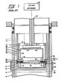
- Fig. 1 shows a typical prior art crystal growing apparatus comprising a
furnace enclosure 10, an EFG crucible/capillary die system comprising acrucible 12, acapillary die 14, a molybdenum orgraphite susceptor 16, after-heater assemblies stem 24 connected to apulling mechanism 26. Preferably,furnace enclosure 10 is a double-walled structure comprising mutually spaced inner andouter walls 11 and 13.Furnace enclosure 10 is surrounded by a radiofrequency heating coil 28 which is coupled to a controllable radio frequency power supply (not shown) of conventional construction. In use,crucible 12 is loaded with acharge 30 of the material to be grown (e.g., P-type silicon). - The
furnace enclosure 10 is fabricated from a pair of concentric spaced-apartcylindrical quartz tubes 11 and 13. Although not shown in detail, it will be understood that, except for an opening at the top to permit removal of the growing crystalline body by the associated pulling mechanism, plus a port (not shown) at the bottom for introduction of a selected gas such as argon,furnace enclosure 10 is closed top and bottom to permit the atmosphere within the enclosure to be controlled. Crucible 12 is a short, hollow, open-topped right prism or right circular cylinder centrally disposed withinenclosure 10. Capillarydie 14 is an integral part of the sidewall ofcrucible 12, as detailed in U.S. Patent No. 4,230,674 (see also U.S. Patents Nos. 4440728 and 4647437 for related designs). As is well known in the art,capillary die 14 is provided with an end face or edge 32 (Fig. 1) shaped and dimensioned to control the form and size of the grown crystal. Preferablyend face 32 is a hollow thin-walled regular polygon as viewed in plan view.End face 32 is provided with acapillary gap 34 of similar form centered in the end face. A plurality ofelongate slots 35 are formed on the inside of the side wall ofcrucible 12 communicating betweencapillary gap 34 and the interior of the crucible, so that the meltedcharge 30 may flow into the capillary gap wherein it may rise by capillary action to replenish the material onend face 32 as the crystal is grown. It will be recognized by those skilled in the art that this is the arrangement of the embodiment illustrated in Fig. 6 of U.S. Patent No. 4,230,674, although it will also be understood thatdie 14 could be formed separately from the crucible, as set forth, for example, in U.S. Patents Nos. 3687633 and 3591348. - The material of construction of crucible 12 (and die 14) is chosen on the basis of the material to be grown. In a preferred embodiment, silicon is grown, in which case it is preferred that
crucible 12 and die 14 are formed of graphite and the seed is silicon. It will be understood thatcrucible 12 and die 14 could be separate parts of differing composition. For the purpose of the present invention, it should also be understood thatend face 32 of die 14 need not be in the form of a regular polygon in plan view, or indeed polygonal, as long as it is in the form of a closed plane figure. -
Susceptor 16 is typically a short hollow open-topped cylindrical or prismatic body dimensioned to accommodatecrucible 12.Susceptor 16 is supported by apedestal 17 attached to the lower end offurnace enclosure 10. The height ofsusceptor 16 is chosen to permit capillary die 14 to project upward beyond the top of susceptor. In the case of growing silicon bodies,susceptor 16 is fabricated of a material such as molybdenum or graphite, the choice in part depending upon the available excitation frequency of heating coil 28 (e.g., preferably molybdenum for frequencies in the vicinity of 10KHz and graphite for frequencies in the vicinity of 8KHz). - The top of
susceptor 16 supports anouter radiation shield 36.Outer radiation shield 36 is in the form of a thin-walled hollow cylinder or prism of similar shape and outside dimension assusceptor 16 and with aninterior flange 37 of similar form as end face 32 of capillary die 14.Outer radiation shield 36 is dimensioned and disposed such thatflange 37 is substantially coplanar with but separated fromend face 32. In growing silicon, it is preferred that the outer radiation shield be fabricated of molybdenum or graphite. Mounted to the interior of capillary die 14 isinner radiation shield 38.Inner radiation shield 38 is formed of one or more annular graphite plates held together in parallel spaced apart opposing relationship. The outside dimension ofinner radiation shield 38 is of similar form as but smaller than the inside dimension ofend face 32.Radiation shield 38 is supported in spaced-apart relationship from die 14 by a plurality ofpins 40 disposed about the inner periphery of thedie 14.Radiation shield 38 is provided with or defines a centralcircular aperture 39. In a preferred embodiment,inner radiation shield 38 is machined from a single piece of graphite, although it will be understood it could be fabricated from a number of sheets fastened together. - A pair of after-
heaters end face 32. After-heater 18 is disposed outside of the die face, while after-heater 20 is disposed inside. After-heater 18 is of hollow, open ended right prismatic form, its base being similar in configuration to dieend face 32. The corresponding faces or sides of after-heater 18 are arranged parallel to the corresponding sides of the octagon formed byend face 32 and extend substantially normal to the plane of the end face. After-heater assembly 18 is a double walled structure, with a graphiteinterior wall 42 and an external carbon felt insulatingwall 44. After-heater 18 is supported and separated fromflange 37 onouter radiation shield 36 by a plurality ofpins 46. - Hollow inner after-
heater 20 includes acylindrical wall 48,top plate 50 and taperedsection 52.Cylindrical wall 48 is a thin-walled hollow graphite right circular cylinder of smaller outside diameter than the circle which can be inscribed within the plan or cross-sectional configuration of end face 32 ofdie 14. Preferably,top plate 50 is a circular graphite plate dimensioned to fit and close off one end ofcylindrical wall 48.Tapered section 52 is in the form of a hollow-open ended conical frustrum attached by its larger base to the other end ofcylindrical wall 48. The smaller base of taperedsection 52 is chosen to be of similar diameter ascircular aperture 39 ininner radiation shield 38. With the exception of the top of inner after-heater 20, the walls of each section are single. The top of inner after-heater 20 is of double-walled construction,top plate 50 supporting a somewhat smaller diameter carbon feltinsulation pad 54. Inner after-heater 20 is supported on the top ofinner radiation shield 38 by taperedsection 52 such that the interior of the after-heater communicates with the interior ofcrucible 12 throughaperture 39 inradiation shield 38.Cylindrical section 48 of the inner after-heater 20 is disposed with its cylindrical axis substantially normal to the plane ofend face 32. - Seed assembly 22 comprises a
seed holder 56 and aseed 58.Seed holder 56 is a plate, preferably of graphite, of similar size and shape as the inside periphery of end face 32 ofdie 14.Seed holder 56 surrounds and rests on a flange 64 onstem 24.Seed holder 56 has a plurality ofopenings flange 56 hasopenings 59 that communicate withholes 57. These holes permit flow of gas upwardly within the growing hollow body.Stem 24 has apassageway 25 for introducing a gas into the space surrounded byseed 58 and the growing hollow body viaopenings -
Seed 58 is eight-sided and may constitute a short length of a crystalline body previously grown according to this invention; alternativelyseed 58 may be formed from a polygonal array of a plurality of rectangular sheets or ribbons having a thickness on the order of, but typically somewhat greater than, the thickness of the desired grown crystal. - A further description of the structural details of a seed assembly can be found in U.S. Patents Nos. 4440728 and 4544528 issued to Stormont et al.
- Initially, stem 24 is affixed by any one of a number of conventional clamping means (not shown) to pulling
mechanism 26, the whole being adjusted to supportseed holder 56 andseed 58 so that the side walls ofseed 58 are coaxial with and in opposing parallel relationship to corresponding faces of inner after-heater 20 and outer after-heater 10. From this position, pullingmechanism 26 may be extended, loweringstem 24 andseed holder 56 towardcrucible 12 and loweringseed 58 towarddie end face 32. - To initiate the growth
sequence pulling mechanism 26 is used tolower seed 58 into contact withdie end face 32 beforeseed holder 56contacts insulation pad 54 atop after-heater 20.Seed 58 is now in position to initiate growth. Ifdie end face 32 is heated above the melting point of the material ofseed 58, the portion of the seed contacting the die end face will melt, wetting the end face and flowing intocapillary gap 34. Pullingmechanism 26 is activated to raisestem 24 and the captivated seed assembly 22. Asseed 58 rises from the die, the melted seed material wetting the die end face is drawn out, by surface tension, into a thin film between the seed and the die end face. Previously meltedcharge 30 rises by capillary action to replenish the material on the die end face. Themolten charge 30 is maintained at a temperature of about 30 degrees C above its melting point, while the temperature atdie end face 32 is kept at a temperature at about 20 degrees C above the melting point. -
Seed 58 is pulled away from die end face 31 at a selected pulling speed, e.g., about 1.8 cm./minute. The pulling speed is set according to the rate at which the latent heat of fusion is removed from the ribbon at the crystallization front, i.e., the interface between the growing ribbon and the melt film at the upper end face 32 of the die/crucible assembly. A crystal is continuously grown onseed 58 at the upper end of the die/crucible assembly and the melt consumed in formation of the silicon body is replaced by upward flow of the melt from the crucible via the capillary. - Thermal control of the growing crystal is provided by
RF heater 28 and after-heaters heaters heater 20 receives radiation from the melt throughaperture 39 ininner radiation shield 38. After-heaters coil 28. In addition to energy transfer by radiation, after-heaters heaters aperture 39, and the amount of insulation afforded by carbon feltwalls tapered section 52 and the growing crystal can be used to provide a growing zone of substantially constant temperature in the vicinity of theend face 32. - According to the usual mode of operation of growing crystals by the EFG process herein above described, argon gas (usually but not necessarily containing a small amount of oxygen) is passed upward in the furnace on a continuous basis at relatively high rates (calculated to provide between about 15-25 volume changes of gas per hour) via an
annular passageway 60 that surrounds the outside wall ofcrucible 12 into the region of the liquid/solid interface, which is sometimes referred to as the "growth zone".Passageway 60 communicates with a gas inlet port (not shown) in the lower end offurnace enclosure 10. The gas rate is generally calculated so as not to disturb the crystallization front while assuring that any volatile impurities in the region of the growth zone will be swept out of the furnace so as to reduce the likelihood of the same being picked up by the growing crystal. The gas is generally introduced at room temperature and flows upward frompassageway 60 betweenpins 46 into the space betweenseed 58 and outer after-heater 18. The gas is then conveyed out of the top end of the furnace. The gas tends to have the added effect of causing some cooling of the growing crystal. To the extent already described, the apparatus of Fig. 1 is similar to the apparatus illustrated and described in U.S. Patent No. 4544528, issued October 1, 1985 to Richard W. Stormont et al. Additional gas flow within the seed and the growing crystalline body is achieved by passing gas into the furnace viapassageway 25 as previously discussed. - The essence of the present invention is to deliberately introduce impurities into the growth zone and cause them to deposit and diffuse into the surface of the growing crystal to form a P-N junction. Since the crystal grown from boron-doped
charge 30 will be P-type silicon, an opposite conductivity type dopant is required to be diffused into the growing body to form a P-N junction. This is accomplished by disposing a solid source of a selected dopant such as phosphorous, in position to vaporize and diffuse into the growing crystal so as to form an N-type region of shallow depth in the growing crystal while it is still in the furnace. By way of example but not limitation, the dopant source may be a silicon carbide sponge containing silicon pyrophosphate, i.e., SiP₂O₇ or a glass such as aluminum metaphosphate, i.e., Al(PO₃)₃. - Referring now to Fig. 2, the furnace shown therein is exactly as described in the prior art furnace of Fig. 1, except that a
dopant source 62 is attached to agraphite holder 80. The latter is adjustably secured to the wall 11 offurnace enclosure 10 so as to permitdopant source 62 to be moved up or down parallel to the axis ofstem 24. Preferablydopant source 62 is attached to the bottom end ofholder 80 as shown in Fig. 2 so as to maximize its exposure to the growing crystalline body. The solid phosphorous dopant source is positioned above but close to the liquid/solid growth interface. Argon gas is introduced into the furnace enclosure below the crucible and is directed so as to flow upwardly inpassageway 60 between the susceptor and theinner wall 13 of the furnace chamber. As demonstrated by the arrows in Fig. 2, the argon gas flows up along the outer surface of the crucible susceptor and then flows up along both sides ofdopant source 62 and itsholder 80 between the growing crystalline body and the outer after-heater. Abaffle 82 is preferably interposed between outer afterheater 18 and theinterior furnace wall 13 so as to limit or totally prevent upward flow of argon gas between the outer after-heater andwall 13, thereby forcing the upwardly flowing gas to pass between the upper end ofsusceptor 16 and the lower end of the outer after-heater into theannular space 83 between the outer after-heater and the crystalline body growing onseed 58. Concurrent flow of argon gas upwardly along the inner side of the growing crystalline body is achieved by introducing a stream of gas intopassageway 25. Some of that inner stream of gas flows down betweenradiation shield 38 and the upper end of the die/crucible assembly so as to cover she upper surface ofmelt 30. However, most of that inner stream flows upwardly viaholes seed 58 and the growing crystalling body. - In growing a hollow silicon body, e.g., a nonagon, the temperature at the upper end of the EFG die is kept at about 1200 degrees C, with the temperature along the growing body decreasing with increasing distance from the growth interface. The dopant source is positioned at a height where the temperature is sufficient to drive the dopant out of the source and cause it to diffuse into the growing P-type silicon body. The rate of diffusion of the dopant into the silicon body is controlled in part by the temperature in the region of the dopant source and also by the pulling speed of the growing body. The higher the dopant source is positioned relative to the height of the growth interface, the lower the driving temperature available for diffusion and the lower the rate of diffusion of phosphorous into the silicon body. Preferably the dopant source is positioned at a height where the average temperature is between about 975 and 1100 degrees C. While the rate of gas flow past the growing silicon body has some effect on the diffusion rate, that effect is not significant in comparison to the temperature of the dopant source and the pulling speed. Furthermore, upward flow of the inert purge gas will prevent the dopant from contaminating the silicon melt when using continuous melt replenishment.
- As a consequence of this step, phosphorous is diffused into the outside surface of the P-type crystalline body so as to form a relatively shallow N region or zone. Typically the N-type region will have a depth of between 0.3 and 0.7 microns.
- Thereafter the hollow body is cut into ribbons. The ribbons require no further trimming since the P-N junction has been formed on only one side.
- The ribbons may be cut in any of a variety of ways well known in the art. For example, a laser cutting tool may be used to subdivide the hollow octagon. Another possible method is by etching. One etch cutting technique involves coating the outer surface of each side of the silicon body with a conventional positive resist material, exposing straight and narrow longitudinally-extending portions of the resist layer to a narrow beam of light, developing the resist using a preferential solvent or etchant such as methyl isobutyl ketone so that the unexposed portions of the resist coating remain intact while the exposed areas are dissolved away to expose narrow line portions of each side wall of the silicon body, and then applying a silicon etchant to the hollow body so as to subdivide it along its exposed areas. KOH or a mixture of one part HF and three parts HNO₃ may be used as the silicon etchant. The excision of the silicon body is followed by rinsing the resulting ribbons with distilled water and then removing residual resist coating with a suitable solvent such as trichloroethylene. Thereafter, the ribbons may be used to form solar cells.
- To make a solar cell requires the final step of applying electrodes to the opposite sides of ribbon. The electrodes are formed by a conventional metallization technique. Preferably, but not necessarily, the metallization involves coating the entire expanse of the P-conductivity side of the ribbon with a continuous adherent coating of aluminum, then coating both the N and P sides of the ribbon with one or more layers of nickel, and thereafter over-coating the nickel layers with successive layers of copper and tin. The electrode formed on the N-conductivity side of the ribbon has the form of a multi-fingered grid, e.g., in the pattern shown in U.S. Patent No. 3,886,036 or 3,811,954, so that a major portion of that surface is uncovered and exposed to receive solar radiations. The resulting structure is a solar cell with a substantially planar P-N junction that lies close to the upper surface of the cell and electrodes for coupling the cell into an electrical unit. By way of example, the electrodes may be formed according to the process described in U.S. Patent No. 4,321,283 issued March 23, 1982 to Kirit 8. Patel et al, or the process described in U.S. Patent No. 4,451,969 issued June 5, 1984 to Arup R. Chaudhuri.
- Following is an example of how to practice the invention according to a preferred embodiment of the invention.
- The crucible and die arrangement shown in Fig. 2 is used to produce a P-type silicon hollow octagon with a wall width of about 10.2 cm (about 4 inches) and a wall thickness of about 0.25 cm (about 0.010 inch). A solid phosphorous doping source in the form of a silicon carbide sponge containing silicon pyrophosphate (SiP₂O₇) is provided at 62.
Source 62 is positioned between the silicon seed and the outer after-heater at a selected level so that the solid phosphorous experiences in excess of 1000 degrees C as a silicon body is being grown onto the seed. Argon gas is fed into thepassageways surface 32. Themolten silicon charge 30 in the crucible is maintained at a temperature of about 30C degrees above its melting point and the temperature of the upper end face 32 ofdie 14 is kept at about 20 degrees above the melting point of silicon. The seed is contacted with the upper end face 32 ofdie 14 long enough to form a film of meet, and then the seed is withdrawn to permit crystal growth to occur. Once growth has commenced the pulling speed is held at about 1.8 cm/minute. Growth continues until substantially all the silicon within the crucible is consumed. The rate of flow of argon gas is then increased to prevent additional diffusion of phosphorous into the silicon octagon. An N-type layer or zone is formed to a depth of about 0.3 microns beneath the octagon's surface. - It is to be understood that the term "crystalline body" as used herein is intended to embrace a crystalline body of a semiconductor material that is polycrystalline or is comprised of a single crystal or two or more crystals, e.g., a bicrystal or tricrystal, growing together longitudinally but separated by a relatively small angle (i.e., less than about 4 degrees) grain boundary.
- Of course, the invention may be practiced by using N-type silicon and a P-type source so as to introduce a P-type layer or zone to the silicon, thereby providing a useful P-N junction.
- Liquid dopants also may be used. In such use a porous reticulated vitreous carbon may be incorporated with liquid dopant. The latter approach is attractive because of the possibility that the liquid dopants can be replenished with ease in this material.
- As a further possible modification, the crucible may be provided with a hollow center riser to define a passageway whereby additional silicon may be supplied to replenish
melt 30. The latter form of crucible and a suitable mechanism for feeding additional source material to the crucible are shown in U.S. Patent No. 4661324. A gas such as argon, or argon mixed with oxygen, may be supplied to the crucible via the center riser, and such gas will flow up out of the crucible into the space betweenseed 58 and the inner after-heater, with that gas flow occurring throughholes - Since changes may be made in the above processes without departing from the scope of the invention herein involved, it is intended that all matter contained in the above description or shown in the accompanying drawing shall be interpreted as illustrative. The present invention is indicated by the broad general meaning of the terms in which the appended claims are expressed.
Claims (31)
Applications Claiming Priority (2)
| Application Number | Priority Date | Filing Date | Title |
|---|---|---|---|
| US07/271,514 US5106763A (en) | 1988-11-15 | 1988-11-15 | Method of fabricating solar cells |
| US271514 | 1988-11-15 |
Publications (3)
| Publication Number | Publication Date |
|---|---|
| EP0369574A2 true EP0369574A2 (en) | 1990-05-23 |
| EP0369574A3 EP0369574A3 (en) | 1991-04-10 |
| EP0369574B1 EP0369574B1 (en) | 1995-01-04 |
Family
ID=23035912
Family Applications (1)
| Application Number | Title | Priority Date | Filing Date |
|---|---|---|---|
| EP89307405A Expired - Lifetime EP0369574B1 (en) | 1988-11-15 | 1989-07-20 | An improved method of fabricating solar cells |
Country Status (5)
| Country | Link |
|---|---|
| US (1) | US5106763A (en) |
| EP (1) | EP0369574B1 (en) |
| JP (1) | JP3002479B2 (en) |
| AU (1) | AU621647B2 (en) |
| DE (1) | DE68920414T2 (en) |
Cited By (3)
| Publication number | Priority date | Publication date | Assignee | Title |
|---|---|---|---|---|
| EP0908958A1 (en) * | 1997-10-01 | 1999-04-14 | Ebara Solar Inc | In-situ diffusion of dopant impurities during dendritic web growth of crystal ribbon |
| US6143633A (en) * | 1995-10-05 | 2000-11-07 | Ebara Solar, Inc. | In-situ diffusion of dopant impurities during dendritic web growth of crystal ribbon |
| EP1061160A1 (en) * | 1999-06-17 | 2000-12-20 | Bayer Aktiengesellschaft | Silicon with structural oxygen doping, preparation and application thereof |
Families Citing this family (10)
| Publication number | Priority date | Publication date | Assignee | Title |
|---|---|---|---|---|
| US5037622A (en) * | 1990-07-13 | 1991-08-06 | Mobil Solar Energy Corporation | Wet-tip die for EFG crystal growth apparatus |
| US5454879A (en) * | 1994-03-17 | 1995-10-03 | Bolger; Stephen R. | Helically grown monolithic high voltage photovoltaic devices and method therefor |
| US6139811A (en) * | 1999-03-25 | 2000-10-31 | Ase Americas, Inc. | EFG crystal growth apparatus |
| US6562132B2 (en) | 2001-04-04 | 2003-05-13 | Ase Americas, Inc. | EFG crystal growth apparatus and method |
| DE10311893B3 (en) * | 2003-03-18 | 2004-10-28 | Fraunhofer-Gesellschaft zur Förderung der angewandten Forschung e.V. | Production of silicon thin layer solar cell comprises treating the casing surface of cylindrical silicon crystal to form boundary layer and transferring outer layer lying on the casing surface onto the substrate |
| JP2005289776A (en) * | 2004-04-05 | 2005-10-20 | Canon Inc | Method for manufacturing crystal and crystal manufacturing apparatus |
| NO322246B1 (en) * | 2004-12-27 | 2006-09-04 | Elkem Solar As | Process for preparing directed solidified silicon ingots |
| US7572334B2 (en) * | 2006-01-03 | 2009-08-11 | Applied Materials, Inc. | Apparatus for fabricating large-surface area polycrystalline silicon sheets for solar cell application |
| DE102006041736A1 (en) | 2006-09-04 | 2008-03-20 | Schott Solar Gmbh | Method and device for producing a pipe |
| US7569462B2 (en) * | 2006-12-13 | 2009-08-04 | Applied Materials, Inc. | Directional crystallization of silicon sheets using rapid thermal processing |
Citations (2)
| Publication number | Priority date | Publication date | Assignee | Title |
|---|---|---|---|---|
| US4036666A (en) * | 1975-12-05 | 1977-07-19 | Mobil Tyco Solar Energy Corporation | Manufacture of semiconductor ribbon |
| US4544528A (en) * | 1981-08-03 | 1985-10-01 | Mobil Solar Energy Corporation | Apparatus for growing tubular crystalline bodies |
Family Cites Families (7)
| Publication number | Priority date | Publication date | Assignee | Title |
|---|---|---|---|---|
| US2841860A (en) * | 1952-08-08 | 1958-07-08 | Sylvania Electric Prod | Semiconductor devices and methods |
| US2854363A (en) * | 1953-04-02 | 1958-09-30 | Int Standard Electric Corp | Method of producing semiconductor crystals containing p-n junctions |
| NL270665A (en) * | 1960-10-31 | 1900-01-01 | ||
| US4056404A (en) * | 1976-03-29 | 1977-11-01 | Mobil Tyco Solar Energy Corporation | Flat tubular solar cells and method of producing same |
| DE2914506A1 (en) * | 1979-04-10 | 1980-10-16 | Siemens Ag | METHOD FOR PRODUCING LARGE-SCALE, PLATE-SHAPED SILICON CRYSTALS WITH A COLUMNAR STRUCTURE |
| DE3049376A1 (en) * | 1980-12-29 | 1982-07-29 | Heliotronic Forschungs- und Entwicklungsgesellschaft für Solarzellen-Grundstoffe mbH, 8263 Burghausen | METHOD FOR PRODUCING VERTICAL PN TRANSITIONS WHEN DRAWING SILICO DISC FROM A SILICONE MELT |
| JPS57132372A (en) * | 1981-02-09 | 1982-08-16 | Univ Tohoku | Manufacture of p-n junction type thin silicon band |
-
1988
- 1988-11-15 US US07/271,514 patent/US5106763A/en not_active Expired - Fee Related
-
1989
- 1989-07-20 DE DE68920414T patent/DE68920414T2/en not_active Expired - Fee Related
- 1989-07-20 EP EP89307405A patent/EP0369574B1/en not_active Expired - Lifetime
- 1989-08-09 AU AU39467/89A patent/AU621647B2/en not_active Ceased
- 1989-09-20 JP JP1244896A patent/JP3002479B2/en not_active Expired - Fee Related
Patent Citations (2)
| Publication number | Priority date | Publication date | Assignee | Title |
|---|---|---|---|---|
| US4036666A (en) * | 1975-12-05 | 1977-07-19 | Mobil Tyco Solar Energy Corporation | Manufacture of semiconductor ribbon |
| US4544528A (en) * | 1981-08-03 | 1985-10-01 | Mobil Solar Energy Corporation | Apparatus for growing tubular crystalline bodies |
Non-Patent Citations (3)
| Title |
|---|
| ELECTRONICS INTERNATIONAL, vol. 54, no. 12, June 1981, pages 39-40; L. LOWE: "Laser pulses create junctions in silicon-ribbon solar cells". * |
| JOURNAL OF CRYSTAL GROWTH, vol. 82, nos. 1,2, March 1987, pages 134-141; A.S. TAYLOR et al.: "Long Nonagons-An approach to high productivity silicon sheet using the EFG method". * |
| JOURNAL OF THE ELECTROCHEMICAL SOCIETY, vol. 131, no. 10, October 1984; pages 2438-2441; K.S. TARNEJA et al.: "Investigation of liquid dopants for the production of high efficiency solar cells from dendritic web silicon". * |
Cited By (3)
| Publication number | Priority date | Publication date | Assignee | Title |
|---|---|---|---|---|
| US6143633A (en) * | 1995-10-05 | 2000-11-07 | Ebara Solar, Inc. | In-situ diffusion of dopant impurities during dendritic web growth of crystal ribbon |
| EP0908958A1 (en) * | 1997-10-01 | 1999-04-14 | Ebara Solar Inc | In-situ diffusion of dopant impurities during dendritic web growth of crystal ribbon |
| EP1061160A1 (en) * | 1999-06-17 | 2000-12-20 | Bayer Aktiengesellschaft | Silicon with structural oxygen doping, preparation and application thereof |
Also Published As
| Publication number | Publication date |
|---|---|
| EP0369574A3 (en) | 1991-04-10 |
| US5106763A (en) | 1992-04-21 |
| EP0369574B1 (en) | 1995-01-04 |
| AU3946789A (en) | 1990-05-24 |
| DE68920414T2 (en) | 1995-05-11 |
| JPH02152225A (en) | 1990-06-12 |
| DE68920414D1 (en) | 1995-02-16 |
| JP3002479B2 (en) | 2000-01-24 |
| AU621647B2 (en) | 1992-03-19 |
Similar Documents
| Publication | Publication Date | Title |
|---|---|---|
| US5156978A (en) | Method of fabricating solar cells | |
| US5106763A (en) | Method of fabricating solar cells | |
| US8591851B2 (en) | Methods and apparatuses for manufacturing cast silicon from seed crystals | |
| US6815605B1 (en) | Silicon single crystal and wafer doped with gallium and method for producing them | |
| US6596075B2 (en) | Method of producing a crystal sheet, apparatus for use in producing the same, and solar cell | |
| US4594229A (en) | Apparatus for melt growth of crystalline semiconductor sheets | |
| US4056404A (en) | Flat tubular solar cells and method of producing same | |
| KR20150103703A (en) | Indium-doped silicon wafer and solar cell using the same | |
| US4036666A (en) | Manufacture of semiconductor ribbon | |
| US4152536A (en) | Solar cells | |
| JP2004140120A (en) | Polycrystalline silicon substrate | |
| US20060225775A1 (en) | Solar cell | |
| US4095329A (en) | Manufacture of semiconductor ribbon and solar cells | |
| Belouet | Growth of silicon ribbons by the RAD process | |
| US6824609B2 (en) | Liquid phase growth method and liquid phase growth apparatus | |
| EP1063706A2 (en) | Ga-doped multicrystalline silicon, Ga-doped multicrystalline silicon wafer and method for producing the same | |
| US4119744A (en) | Method of manufacturing semiconductor devices in which a layer of semiconductor material is provided on a substrate | |
| JP2001064007A (en) | Ga-ADDED POLYCRYSTALLINE SILICON, Ga-ADDED POLYCRYSTALLINE SILICON WAFER AND ITS PRODUCTION | |
| JP2002237465A (en) | Method for manufacturing solid-phase sheet | |
| JP2004140087A (en) | Polycrystalline silicon substrate for solar cell and method for manufacturing the same, and method for manufacturing solar cell using the substrate | |
| JP4282278B2 (en) | Substrate, plate manufacturing method using the substrate, plate and solar cell produced from the plate | |
| US4125425A (en) | Method of manufacturing flat tapes of crystalline silicon from a silicon melt by drawing a seed crystal of silicon from the melt flowing down the faces of a knife shaped heated element | |
| JP4188725B2 (en) | Method for producing plate-like silicon, base plate for producing plate-like silicon, plate-like silicon and solar cell using the plate-like silicon | |
| JP3212725B2 (en) | Liquid phase growth method and liquid phase growth apparatus | |
| Janz et al. | High quality silicon films from halogen lamp melting for new thin-film solar cell and module concepts |
Legal Events
| Date | Code | Title | Description |
|---|---|---|---|
| PUAI | Public reference made under article 153(3) epc to a published international application that has entered the european phase |
Free format text: ORIGINAL CODE: 0009012 |
|
| AK | Designated contracting states |
Kind code of ref document: A2 Designated state(s): DE FR GB IT |
|
| PUAL | Search report despatched |
Free format text: ORIGINAL CODE: 0009013 |
|
| AK | Designated contracting states |
Kind code of ref document: A3 Designated state(s): DE FR GB IT |
|
| 17P | Request for examination filed |
Effective date: 19911005 |
|
| 17Q | First examination report despatched |
Effective date: 19920901 |
|
| GRAA | (expected) grant |
Free format text: ORIGINAL CODE: 0009210 |
|
| AK | Designated contracting states |
Kind code of ref document: B1 Designated state(s): DE FR GB IT |
|
| REF | Corresponds to: |
Ref document number: 68920414 Country of ref document: DE Date of ref document: 19950216 |
|
| ET | Fr: translation filed | ||
| ITF | It: translation for a ep patent filed |
Owner name: ING. DORIGUZZI ANDREA |
|
| PGFP | Annual fee paid to national office [announced via postgrant information from national office to epo] |
Ref country code: FR Payment date: 19950629 Year of fee payment: 7 |
|
| PLBE | No opposition filed within time limit |
Free format text: ORIGINAL CODE: 0009261 |
|
| STAA | Information on the status of an ep patent application or granted ep patent |
Free format text: STATUS: NO OPPOSITION FILED WITHIN TIME LIMIT |
|
| 26N | No opposition filed | ||
| REG | Reference to a national code |
Ref country code: FR Ref legal event code: CD |
|
| PG25 | Lapsed in a contracting state [announced via postgrant information from national office to epo] |
Ref country code: FR Effective date: 19970328 |
|
| REG | Reference to a national code |
Ref country code: FR Ref legal event code: ST |
|
| REG | Reference to a national code |
Ref country code: GB Ref legal event code: IF02 |
|
| PGFP | Annual fee paid to national office [announced via postgrant information from national office to epo] |
Ref country code: GB Payment date: 20020621 Year of fee payment: 14 |
|
| PGFP | Annual fee paid to national office [announced via postgrant information from national office to epo] |
Ref country code: DE Payment date: 20020729 Year of fee payment: 14 |
|
| PG25 | Lapsed in a contracting state [announced via postgrant information from national office to epo] |
Ref country code: GB Free format text: LAPSE BECAUSE OF NON-PAYMENT OF DUE FEES Effective date: 20030720 |
|
| PG25 | Lapsed in a contracting state [announced via postgrant information from national office to epo] |
Ref country code: DE Free format text: LAPSE BECAUSE OF NON-PAYMENT OF DUE FEES Effective date: 20040203 |
|
| GBPC | Gb: european patent ceased through non-payment of renewal fee |
Effective date: 20030720 |
|
| PG25 | Lapsed in a contracting state [announced via postgrant information from national office to epo] |
Ref country code: IT Free format text: LAPSE BECAUSE OF NON-PAYMENT OF DUE FEES;WARNING: LAPSES OF ITALIAN PATENTS WITH EFFECTIVE DATE BEFORE 2007 MAY HAVE OCCURRED AT ANY TIME BEFORE 2007. THE CORRECT EFFECTIVE DATE MAY BE DIFFERENT FROM THE ONE RECORDED. Effective date: 20050720 |