EP0368013A1 - Circuit for an adaptive comb filter for separating the luminance and chrominance signals of a composite PAL or NTSC video signal - Google Patents
Circuit for an adaptive comb filter for separating the luminance and chrominance signals of a composite PAL or NTSC video signal Download PDFInfo
- Publication number
- EP0368013A1 EP0368013A1 EP89118869A EP89118869A EP0368013A1 EP 0368013 A1 EP0368013 A1 EP 0368013A1 EP 89118869 A EP89118869 A EP 89118869A EP 89118869 A EP89118869 A EP 89118869A EP 0368013 A1 EP0368013 A1 EP 0368013A1
- Authority
- EP
- European Patent Office
- Prior art keywords
- signal
- color
- circuit
- beard
- comb
- Prior art date
- Legal status (The legal status is an assumption and is not a legal conclusion. Google has not performed a legal analysis and makes no representation as to the accuracy of the status listed.)
- Granted
Links
Images


Classifications
-
- H—ELECTRICITY
- H04—ELECTRIC COMMUNICATION TECHNIQUE
- H04N—PICTORIAL COMMUNICATION, e.g. TELEVISION
- H04N9/00—Details of colour television systems
- H04N9/77—Circuits for processing the brightness signal and the chrominance signal relative to each other, e.g. adjusting the phase of the brightness signal relative to the colour signal, correcting differential gain or differential phase
- H04N9/78—Circuits for processing the brightness signal and the chrominance signal relative to each other, e.g. adjusting the phase of the brightness signal relative to the colour signal, correcting differential gain or differential phase for separating the brightness signal or the chrominance signal from the colour television signal, e.g. using comb filter
Definitions
- the color beard signal in the form of the quadrature modulated color carrier F, the luminance signal Y, the blanking signal A and the synchronous signal S are transmitted as a combined so-called FBAS signal.
- the luminance signal and the color beard signal are nested in terms of frequency. In practice it is often necessary to separate the luminance signal on the one hand and the color beard signal on the other hand in order to feed these signals to separate signal paths for further processing or image reproduction. The separation is also necessary in a video recorder because the color-beard signal is subjected to a special conversion there.
- the invention has for its object to develop a comb filter of the type described so that interference effects are largely avoided with good signal separation.
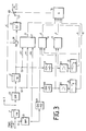
- FIG. 1 shows the principle of an adaptive comb filter circuit on the basis of a block diagram.
- Fig.1A for signals according to PAL
- Fig.1B for signals according to NTSC.
- Auxiliary circuits phase, transit time, amplitude correction, etc., which are necessary for the function of the circuit, but do not contribute to an understanding of the principle, are not taken into account in the illustration.
- blocks 4 and 5 there are controllable switches K1 and K2, by means of which the respective chrominance signal path is selected. The switching state of these switches is controlled by a signal evaluation circuit contained in block 6, the phase states of the signals S1, S2 and S3 present on the 1H delay lines 1 and 2 being evaluated for the output of the switching signals.
- the NTSC / FBAS signal present at the input is fed to an input of the subtracting stage 3 via a broadband 1-line delay line 1 in block 5.
- the comb filtering for the chrominance signal C1 is carried out by means of a second, narrow-band 1-line delay line 2 in connection with subtracting stage 18, which is connected in series with an upstream bandpass filter of the first delay line 1.
- the delay line 1, which is not necessary for the NTSC comb filter, is required in order to obtain an undelayed signal S1 in analogy to FIG. 1A.
- This can be the color carrier signal or the bandpass filter be luminance signal.
- This signal is used in the evaluation circuit contained in block 6 for the comparison with the signal S2 delayed by one line and the signal S3 delayed by 2 lines.
- a switching voltage is emitted by the evaluation circuit 6, by means of which the color key signal C, C1, which corresponds to the optimal conditions for forming the luminance signal Y, is selected in block 5 by means of the switch K5 and supplied to the subtracting stage
- Switch signals A, B, D and F are generated according to predetermined criteria, which correspond to the input of the "AND” Circuit 16 are supplied.
- the further “AND” circuit 17 is driven by the inverted output signal from circuit 16 and by the switching signal E generated in the evaluation circuit 8.
- the switching of the signal paths is effected by switches K3 and K4, which are controlled by the output signals of the "AND” circuits. It applies that the switches are open with an H signal.
- disturbances of conventional comb filters can be avoided in that the adaptive control with the help of a special evaluation circuit, which recognizes all vertical signal jumps, switches from the comb-filtered signal C1 to the band-pass filtered signal C or, if necessary, the color-beard signal completely switches off.
- the comb-filtered color beard signal is taken from the output of the subtracting stage 18, the inputs of which are supplied with the bandpass-filtered and the color beard signal delayed by two lines.
- the resistors 19 and 20 serve for decoupling and the amplification stage 21 for amplitude adjustment.
- Switch signals A, B, C, D and F are generated according to predetermined criteria and are supplied to the input of the "AND" circuit 16 will.
- the switching of the signal paths is effected by switch K5, which is controlled by the output signal of the "AND" circuit 16. It applies that switch K5 is applied to signal C1 in the case of an H signal and signal C in the case of an L signal.
- disturbances of conventional comb filters can be avoided in that the adaptive control with the help of a special evaluation circuit, which detects all vertical signal jumps, at each this jumps from the comb-filtered signal C1 to the band-pass filtered signal C.
- the comb-filtered color-beard signal C1 is taken from the output of the subtracting stage 18, the inputs of which are fed to the non-delayed and the color-beard signal of the stage 2 delayed by one line.
- the amplification stage 21 is used to adjust the amplitude.
- FIGS. 2 and 3 are examples of several conceivable circuit variants. They can be implemented in both analog and digital form. It is also possible to combine the circuits in an integrated circuit.
Abstract
Description
Bei Farbfernsehsystemen nach PAL oder NTSC wird das Farbartsignal in Form des quadratur modulierten Farbträgers F, das Leuchtdichtesignal Y, das Austastsignal A und das Synchronsignal S als kombiniertes sogenanntes FBAS-Signal übertragen. Dabei sind das Leuchtdichtesignal und das Farbartsignal frequenzmäßig verschachtelt. In der Praxis ist es häufig notwendig, das Leuchtdichtesignal einerseits und Farbartsignal andererseits zu trennen, um diese Signale getrennten Signalwegen für die Weiterverarbeitung oder die Bildwiedergabe zuzuführen. Die Trennung ist auch notwendig in einem Videorecorder, weil dort das Farbartsignal einer besonderen Umwandlung unterworfen wird.In color television systems according to PAL or NTSC, the color beard signal in the form of the quadrature modulated color carrier F, the luminance signal Y, the blanking signal A and the synchronous signal S are transmitted as a combined so-called FBAS signal. The luminance signal and the color beard signal are nested in terms of frequency. In practice it is often necessary to separate the luminance signal on the one hand and the color beard signal on the other hand in order to feed these signals to separate signal paths for further processing or image reproduction. The separation is also necessary in a video recorder because the color-beard signal is subjected to a special conversion there.
Es ist bekannt, das vom Leuchtdichtesignal über einen Bandpaß abgetrennte Farbartsignal einer Zeilenverzögerung zu unterziehen, und durch Kombination der Signale vom Eingang und Ausgang der Zeilenverzögerung ein kammgefiltertes Farbartsignal zu gewinnen. Das reine Leuchtdichtesignal wird dadurch gewonnen, daß von dem kombinierten FBAS-Signal das extrahierte, kammgefilterte Farbartsignal subtrahiert wird. Bei einem derartigen Kammfilter kommt es zwangsläufig zu einer Mittlung über mehrere Zeilen, weil Signale aufeinanderfolgender Zeilen addiert werden. So werden z.B. bei einem PAL-Signal bei allen hochfrequenten Signalsprüngen bzw. Farbübergängen in vertikaler Richtung jeweils die ersten zwei Zeilen, sowie zwei Zeilen nach dem "HF-Signal" gestört, wie in der folgenden Auflistung dargestellt.

Für verbesserte Übertragungssysteme wie z.B. bei Recordern nach dem S-VHS-System oder bei hochauflösenden Fernsehsystemen, werden an ein Kammfilter aber erhöhte Anforderungen gestellt.For improved transmission systems such as in the case of recorders based on the S-VHS system or in the case of high-definition television systems, increased demands are placed on a comb filter.
Der Erfindung liegt die Aufgabe zugrunde, ein Kammfilter der beschriebenen Art so weiterzubilden, daß bei guter Signaltrennung Störeffekte weitgehendst vermieden werden.The invention has for its object to develop a comb filter of the type described so that interference effects are largely avoided with good signal separation.
Diese Aufgabe wird gemäß der Erfindung durch die im Anspruch 1 aufgeführten Merkmale gelöst. Vorteilhafte Weiterbildungen der Erfindung sind in den Unteransprüchen gekennzeichnet.This object is achieved according to the invention by the features listed in
Im Prinzip wird bei den die beschriebenen Fehler bewirkenden Merkmalen inerhalb einer Bildstruktur der Subtrahierstufe zur Erzeugung des reinen Leuchtdichtesignales anstelle des kammgefilterten Farbartsignales entweder nur das nicht verzögerte, bandpaßgefilterte Fabartsignal, oder auch in der PAL-Version kein Farbsignal zugeführt. Die Entscheidung, welches der Signale angeschaltet wird, wird durch eine Auswahlschaltung getroffen, deren Wirkungsweise anhand der Figuren beispielhaft näher beschrieben wird.In principle, in the case of the features causing the errors described, within an image structure of the subtracting stage for generating the pure luminance signal, instead of the comb-filtered color-beard signal, either only the undelayed bandpass-filtered Fabart signal or also no color signal is supplied in the PAL version. The decision as to which of the signals is switched on is made by a selection circuit, the mode of operation of which is described in more detail by way of example with reference to the figures.
Fig. 1 zeigt anhand eines Blockschaltbildes das Prinzip einer adaptiven Kammfilterschaltung. Fig.1A für Signale nach PAL und Fig.1B für Signale nach NTSC. Hilfsschaltungen (Phasen-, Laufzeit-, Amplitudenkorrektur, usw.), die zwar für die Funktion der Schaltung notwendig sind, jedoch zum Verstehen des Prinzips nicht beitragen, werden in der Darstellung nicht berücksichtigt.1 shows the principle of an adaptive comb filter circuit on the basis of a block diagram. Fig.1A for signals according to PAL and Fig.1B for signals according to NTSC. Auxiliary circuits (phase, transit time, amplitude correction, etc.), which are necessary for the function of the circuit, but do not contribute to an understanding of the principle, are not taken into account in the illustration.
In Fig.1A wird das am Eingang anstehende PAL/FBAS-Signal einerseits einem Eingang einer Subtrahierstufe 3 und andererseits über ein Bandpaßfilter einer Auswahlschaltung bestehend aus den Blöcken 4,5 und 6 zugeführt, in welchen nach vorgegebenen Kriterien bestimmt wird, welches Farbartsignal, C1 = zwei Zeilen kammgefiltert, oder C = nur bandpaßgefiltert, der Subtrahierstufe 3 zur Bildung des Leuchdichtesignales Y zugeführt wird. In den Blöcken 4 und 5 sind steuerbare Schalter K1 und K2 vorhanden, durch die der jeweilige Farbartsignalweg selektiert wird. Der Schaltzustand dieser Schalter wird von einer in Block 6 enthaltenen Signalauswerteschaltung gesteuert, wobei die Phasenzustände der an den 1H-Verzögerungsleitungen 1 und 2 anstehenden Signale S1,S2 und S3 für die Ausgabe der Schaltsignale ausgewertet werden.In FIG. 1A, the PAL / FBAS signal present at the input is supplied on the one hand to an input of a
In Fig.1B wird in Block 5 das am Eingang anstehende NTSC/FBAS-Signal über eine breitbandige 1-Zeilen-Verzögerungsleitung 1 einem Eingang der Subtrahierstufe 3 zugeführt. Die Kammfilterung für das Farbartsignal C1 geschieht mittels einer zweiten, schmalbandigen 1-Zeilen-Verzögerungsleitung 2 in Verbindung mit Subtrahierstufe 18, die mit einem vorgeschaltetem Bandpaßfilter der ersten Verzögerungsleitung 1 in Reihe nachgeschaltet ist. Die ansich für das NTSC-Kammfilter nicht nötige Verzögerungsleitung 1 ist erforderlich, um in Analogie zu Fig. 1A ein nicht verzögertes Signal S1 zu erhalten. Dieses kann das Farbträgersignal oder das bandpaßgefil terte Luminanzsignal sein. Dieses Signal wird in der in Block 6 enthaltenen Auswerteschaltung für den Vergleich mit dem um eine Zeile verzögerten Signal S2 und dem um 2 Zeilen verzögerten Signal S3 herangezogen. Von der Auswerteschaltung 6 wird eine Schaltspannung abgegeben, durch die in Block 5 mittels Schalter K5 jeweils dasjenige Farbartsignal C, C1, ausgewählt und der Subtrahierstufe 3 zugeführt wird, welches den optimalen Bedingungen zur Bildung des Leuchtdichtesignales Y entspricht.In FIG. 1B, the NTSC / FBAS signal present at the input is fed to an input of the
Fig. 2 zeigt für ein PAL-Signal anhand eines detaillierten Blockschaltbildes die Signalauswerteschaltung der nach Fig. 1A bezeichneten Blöcke 4,5 und 6. Es werden nach vorgegebenen Kriterien Schaltsignale A,B,D und F generiert, die dem Eingang der "UND"-Schaltung 16 zugeführt werden. Die weitere "UND"-Schaltung 17 wird von dem invertierten Ausgangssignal von Schaltung 16 sowie von dem in der Auswerteschaltung 8 generierten Schaltsignal E angesteuert. Die Umschaltung der Signalwege wird durch Schalter K3 und K4 bewirkt, die von den Ausgangssignalen der "UND"-Schaltungen gesteuert werden. Dabei gilt, daß bei einem H-Signal die Schalter geöffnet sind.2 shows for a PAL signal on the basis of a detailed block diagram the signal evaluation circuit of
Wie in der Beschreibung bereits erwähnt, können Störungen herkömmlicher Kammfilter dadurch vermieden werden, daß die adaptive Steuerung mit Hilfe einer speziellen Auswerteschaltung, die alle vertikalen Signalsprünge erkennt, bei jedem dieser Sprünge vom kammgefilterten Signal C1 auf das bandpaßgefilterte Signal C umschaltet oder ggf. das Farbartsignal komplett abschaltet. Das kammgefilterte Farbartsignal wird vom Ausgang der Subtrahierstufe 18 abgenommen deren Eingänge das bandpaßgefilterte und das um zwei Zeilen verzögerte Farbartsignal zugeführt wird. Die Widerstände 19 und 20 dienen zur Entkopplung und die Verstärkungsstufe 21 der Amplitudenanpassung.As already mentioned in the description, disturbances of conventional comb filters can be avoided in that the adaptive control with the help of a special evaluation circuit, which recognizes all vertical signal jumps, switches from the comb-filtered signal C1 to the band-pass filtered signal C or, if necessary, the color-beard signal completely switches off. The comb-filtered color beard signal is taken from the output of the
Es gibt folgende Schaltkriterien:
- A) Das Kammfilter soll nur eingeschaltet werden, d.h. Ausgabe von Signal C1 (Schaltsignal A = H), wenn nach der 2H-Verzögerung (Signal S3) ein Farbartsignal oder ein hochfrequentes Y-Signal erscheint. Das den Einschaltvorgang auslösende Schaltsignal A kann z.B. wie folgt aus dem Signal S3 gewonnen werden:
- 1. Zweiweggleichrichtung in Block 11
- 2. Verstärkung/Begrenzung in Block 13
- 3. Siebung mit sehr kurzer Zeitkonstante in Block 15.
- B) Das Kammfilter muß ausgeschaltet werden (Schaltsignal B = L), wenn vor der 2H-Verzögerung (Signal S1) kein Farbartsignal oder kein hochfrequentes Y-Signal vorhanden ist. Die Schaltspannung B kann ebenfalls wie unter A) gewonnen werden:
- 1. Zweiweggleichrichtung in Block 10
- 2. Verstärkung/Begrenzung in Block 12
- 3. Siebung mit sehr kurzer Zeitkonstante in Block 14.
- C) Bei Farbwechseln in vertikaler Richtung muß ebenfalls auf das bandpaßgefilterte Signal C (Schaltsignal F = L) umgeschaltet werden. Würden hierzu direkt das OH- und das 2H-verzögerte Signal in der Phase verglichen, so müßte aufgrund des 1/4-Zeilen-Offsets ein Signal invertiert werden. Dadurch wäre jedoch das Kammfilter bei hochfrequenten Y-Signalen ständig ausgeschaltet. Aus diesem Grund wird die Phase der in den Blöcken 10 und 11 zweiweggerichteten Signale S1 und S3 in
Erkennungsschaltung 9 verglichen, von der das Schaltsignal F abgegeben wird. - D) Für einen 180°-Farbsprung, bei dem auch auf das bandpaßgefilterte Signal C geschaltet werden muß (Schaltsignal D = L) ist eine besondere Erkennungsschaltung 7 notwendig, von der die Schaltspannung D abgegeben wird. Hierzu ist eine Aufteilung der 2H-Verzögerungsleitung in zwei 1H-
Leitungen 1,2 erforderlich, um die Phasenlage des um eine Zeile verzögerten Signales S2 erkennen zu können. Wird nun über einer der beiden Leitungen eine Phasendifferenz und gleichzeitig über beide Leitungen Phasengleichheit festgestellt, kann daraus auf einen 180°-Sprung geschlossen werden. (Die gleiche Situation ergibt sich auch noch bei anderen, jedoch nicht praxisrelevanten Signalen.) - E) Erfolgt ein Signalsprung auf ein hochfrequentes Y-Signal, sollte der Farbartsignalausgang völlig abgeschaltet werden. (Schaltsignal E = L). Daß es sich um ein Luminanzsignal handelt, kann frühestens nach einer Zeile durch die Erkennungsschaltung 8 festgestellt werden. D.h., eine Zeile ist zwangsläufig gestört. Anschließend wird bei gleichen Signalen vor und hinter der ersten Verzögerungsleitung (S1 und S2) der Farbartsignalausgang abgeschaltet, wenn gleichzeitig durch die Erkennung nach A) kein Signal detektiert wird.
- A) The comb filter should only be switched on, ie output of signal C1 (switching signal A = H) if a color-beard signal or a high-frequency Y signal appears after the 2H delay (signal S3). Switching signal A which triggers the switch-on process can be obtained from signal S3 as follows:
- 1. Two-way rectification in
block 11 - 2. Reinforcement / limitation in
block 13 - 3. Screening with a very short time constant in
block 15.
- 1. Two-way rectification in
- B) The comb filter must be switched off (switching signal B = L) if there is no color beard signal or no high-frequency Y signal before the 2H delay (signal S1). The switching voltage B can also be obtained as under A):
- 1. Two-way rectification in block 10
- 2. Reinforcement / limitation in
block 12 - 3. Screening with a very short time constant in
block 14.
- C) When changing colors in the vertical direction, you must also switch to bandpass-filtered signal C (switching signal F = L). If the OH and the 2H-delayed signal were compared in phase directly, a signal would have to be inverted due to the 1/4 line offset. However, this would permanently switch off the comb filter for high-frequency Y signals. Out for this reason, the phase of the signals S1 and S3, which are bidirectional in
blocks 10 and 11, is compared indetection circuit 9, from which the switching signal F is emitted. - D) For a 180 ° color jump, in which it is also necessary to switch to the bandpass-filtered signal C (switching signal D = L), a special detection circuit 7 is necessary, from which the switching voltage D is output. For this purpose, a division of the 2H delay line into two 1H
lines 1, 2 is necessary in order to be able to recognize the phase position of the signal S2 delayed by one line. If a phase difference is found over one of the two lines and phase equality is found over both lines at the same time, a 180 ° jump can be inferred from this. (The same situation also arises with other, but not practice-relevant signals.) - E) If there is a signal jump to a high-frequency Y signal, the far-beard signal output should be switched off completely. (Switching signal E = L). That it is a luminance signal can be determined by the detection circuit 8 at the earliest after one line. Ie one line is inevitably disturbed. Then, with the same signals in front of and behind the first delay line (S1 and S2), the chrominance signal output is switched off, if at the same time no signal is detected by the detection according to A).
Für die Erkennungsschaltungen 7,8 und 9 gelten folgende Kriterien:The following criteria apply to the detection circuits 7, 8 and 9:
wenn
φ0 ≠ φ1
(oder
φ1 ≠ φ2)
und
φ0 = φ2
dann D = L
sonst D = Hif
φ0 ≠ φ1
(or
φ1 ≠ φ2)
and
φ0 = φ2
then D = L
otherwise D = H
wenn
φ0 = φ1
und
A = L
dann E = L
sonst E = Hif
φ0 = φ1
and
A = L
then E = L
otherwise E = H
wenn
φ2 = φ0
dann F = H
sonst F = Lif
φ2 = φ0
then F = H
otherwise F = L
Fig. 3 zeigt für ein NTSC-Signal die Signalauswerteschaltung der nach Fig. 1B bezeichneten Blöcke 5 und 6. Es werden nach vorgegebenen Kriterien Schaltsignale A,B,C,D und F generiert, die dem Eingang der "UND"-Schaltung 16 zugeführt werden. Die Umschaltung der Signalwege wird durch Schalter K5 bewirkt, der vom Ausgangssignal der "UND"-Schaltung 16 gesteuert wird. Dabei gilt, daß bei einem H-Signal Schalter K5 an das Signal C1 und bei einem L-Signal an das Signal C angelegt ist.3 shows the signal evaluation circuit of
Wie in der Beschreibung bereits erwähnt, können Störungen herkömmlicher Kammfilter dadurch vermieden werden, daß die adaptive Steuerung mit Hilfe einer speziellen Auswerteschaltung, die alle vertikalen Signalsprünge erkennt, bei jedem dieser Sprünge vom kammgefilterten Signal C1 auf das bandpaßgefilterte Signal C umschaltet. Das kammgefilterte Farbartsignal C1 wird vom Ausgang der Subtrahierstufe 18 abgenommen, deren Eingänge das nicht verzögerte und das um eine Zeile verzögerte Farbartsignal der Stufe 2 zugeführt wird. Die Verstärkungsstufe 21 dient der Amplitudenanpassung.As already mentioned in the description, disturbances of conventional comb filters can be avoided in that the adaptive control with the help of a special evaluation circuit, which detects all vertical signal jumps, at each this jumps from the comb-filtered signal C1 to the band-pass filtered signal C. The comb-filtered color-beard signal C1 is taken from the output of the subtracting
Es gibt folgende Schaltkriterien:
- A,B) Schalter K5 schaltet das kammgefilterte Farbartsignal C1 an (Schaltsignal A = H und/oder B = H) wenn ein hochfrequentes Farbart- oder Y-Signal vorhanden ist. Das Schaltsignal A kann wie folgt aus dem Signal S3 gewonnen werden:
1. Zweiweggleichrichtung inBlock 11
2. Verstärkung/Begrenzung inBlock 13
3. Siebung mit sehr kurzer Zeitkonstante inBlock 15.
Die Schaltspannung B kann ähnlich wie die Schaltspannung A aus dem Signal S2 gewonnen werden
1. Zweiweggleichrichtung in Block 10
2. Verstärkung/Begrenzung inBlock 12
3. Siebung mit sehr kurzer Zeitkonstante inBlock 14. - C) Bei Farbwechseln in vertikaler Richtung (Farbphasensprung) muß das bandpaßgefilterte Signal C (Schaltsignal F = L) angeschaltet werden. Würden hierzu direkt die Signale S2 und S3 in der Phase verglichen, so müßte aufgrund des Zeilen-Offsets ein Signal invertiert werden. Dadurch wäre jedoch das Kammfilter bei hochfrequenten Y-Signa len ständig ausgeschaltet. Aus diesem Grund wird die Phase der in den Blöcken 10 und 11 zweiweggerichteten Signale S1 und S3 in
Erkennungsschaltung 9 verglichen, von der das Schaltsignal F abgegeben wird. - D) Für einen 180°-Farbphasensprung, bei dem auch auf das bandpaßgefilterte Signal C geschaltet werden muß (Schaltsignal D = L), ist eine besondere Erkennungsschaltung 7 notwendig, von der die Schaltspannung D abgegeben wird. Hierzu ist die
Reihenschaltung von zwei 1H-Leitungen, 1,2 erforderlich, um die Phasenlage des um eine Zeile verzögerten Signales S2 sowie des um 2 Zeilen verzögerten Signales S3 erkennen zu können. Wird über Verzögerungsleitung l und gleichzeitig über beide Leitungen 1,2 eine Phasendifferenz festgestellt, kann daraus auf einen 180°-Sprung geschlossen werden. Dies ergibt sich auch, wenn über Leitung 2 Phasengleichheit festgestellt wird. - E) Erfolgt ein Signalsprung von einem tieffrequenten auf ein hochfrequentes Y-Signal, muß ebenfalls das bandpaßgefilterte Signal C angeschaltet werden (Schaltsignal E = L). Bei gleichen Signalen vor und hinter der ersten Verzögerungsleitung 1 und wenn gleichzeitig die Erkennung nach A) kein Signal detektiert wird, ist Schaltsignal E = L.
- A, B) Switch K5 switches on the comb-filtered color tone signal C1 (switching signal A = H and / or B = H) if a high-frequency color type or Y signal is present. Switching signal A can be obtained from signal S3 as follows:
1. Two-way rectification inblock 11
2. Reinforcement / limitation inblock 13
3. Screening with a very short time constant inblock 15.
The switching voltage B can be obtained similarly to the switching voltage A from the signal S2
1. Two-way rectification in block 10
2. Reinforcement / limitation inblock 12
3. Screening with a very short time constant inblock 14. - C) When changing colors in the vertical direction (color phase shift), the bandpass-filtered signal C (switching signal F = L) must be switched on. If the signals S2 and S3 were directly compared in phase for this purpose, a signal would have to be inverted due to the line offset. However, this would make the comb filter with high-frequency Y-Signa len constantly switched off. For this reason, the phase of the two-way signals S1 and S3 in the
blocks 10 and 11 is compared in thedetection circuit 9, from which the switching signal F is emitted. - D) For a 180 ° color phase jump, in which it is also necessary to switch to the bandpass-filtered signal C (switching signal D = L), a special detection circuit 7 is necessary, from which the switching voltage D is output. This requires the series connection of two 1H
lines 1, 2 in order to be able to recognize the phase position of the signal S2 delayed by one line and of the signal S3 delayed by 2 lines. If a phase difference is determined viadelay line 1 and simultaneously over bothlines 1, 2, it can be concluded that there is a jump in 180 °. This also results if phase 2 is determined via line 2. - E) If there is a signal jump from a low-frequency to a high-frequency Y signal, the bandpass-filtered signal C must also be switched on (switching signal E = L). With the same signals in front of and behind the
first delay line 1 and if the detection according to A) is not detected at the same time, the switching signal E = L.
Für die Erkennungsschaltungen 7,8 und 9 gelten folgende Kriterien:The following criteria apply to the detection circuits 7, 8 and 9:
wenn
φ0 ≠ φ1
und
(φ0 ≠ φ2
und/oder
φ1 = φ2
dann D = L
sonst D = Hif
φ0 ≠ φ1
and
(φ0 ≠ φ2
and or
φ1 = φ2
then D = L
otherwise D = H
wenn
φ0 = φ1
und
A = L
dann E = L
sonst E = Hif
φ0 = φ1
and
A = L
then E = L
otherwise E = H
wenn
φ1 ≠ φ2
dann F = L
sonst F = Hif
φ1 ≠ φ2
then F = L
otherwise F = H
Die in Figur 2 und 3 dargestellten Schaltungen sind Beispiele mehrerer denkbarer Schaltungsvarianten. Sie können sowohl in analoger als auch in digitaler Form realisiert werden. Auch ist es möglich, die Schaltungen in einem integrierten Schaltkreis zusammenzufassen.The circuits shown in FIGS. 2 and 3 are examples of several conceivable circuit variants. They can be implemented in both analog and digital form. It is also possible to combine the circuits in an integrated circuit.
Claims (5)
Priority Applications (1)
| Application Number | Priority Date | Filing Date | Title |
|---|---|---|---|
| AT89118869T ATE88849T1 (en) | 1988-10-20 | 1989-10-11 | CIRCUIT FOR AN ADAPTIVE COMB FILTER TO SEPARATE THE LUMINANCE SIGNAL AND THE COLOR SIGNAL OF A CVBS-PAL OR NTSC SIGNAL. |
Applications Claiming Priority (2)
| Application Number | Priority Date | Filing Date | Title |
|---|---|---|---|
| DE3836043 | 1988-10-20 | ||
| DE3836043A DE3836043A1 (en) | 1988-10-20 | 1988-10-20 | CIRCUIT FOR AN ADAPTIVE COMB FILTER FOR THE SEPARATION OF LUMINOUSITY SIGNAL AND COLOR TYPE SIGNAL OF AN FBAS-PAL SIGNAL |
Publications (2)
| Publication Number | Publication Date |
|---|---|
| EP0368013A1 true EP0368013A1 (en) | 1990-05-16 |
| EP0368013B1 EP0368013B1 (en) | 1993-04-28 |
Family
ID=6365704
Family Applications (2)
| Application Number | Title | Priority Date | Filing Date |
|---|---|---|---|
| EP89912235A Pending EP0414830A1 (en) | 1988-10-20 | 1989-10-11 | Adaptive pal or nstc comb filter |
| EP89118869A Expired - Lifetime EP0368013B1 (en) | 1988-10-20 | 1989-10-11 | Circuit for an adaptive comb filter for separating the luminance and chrominance signals of a composite pal or ntsc video signal |
Family Applications Before (1)
| Application Number | Title | Priority Date | Filing Date |
|---|---|---|---|
| EP89912235A Pending EP0414830A1 (en) | 1988-10-20 | 1989-10-11 | Adaptive pal or nstc comb filter |
Country Status (11)
| Country | Link |
|---|---|
| US (1) | US5173768A (en) |
| EP (2) | EP0414830A1 (en) |
| JP (1) | JPH04501347A (en) |
| KR (1) | KR0138101B1 (en) |
| AT (1) | ATE88849T1 (en) |
| AU (1) | AU4493789A (en) |
| DE (2) | DE3836043A1 (en) |
| DK (1) | DK69691A (en) |
| ES (1) | ES2040960T3 (en) |
| HK (1) | HK135693A (en) |
| WO (1) | WO1990004906A1 (en) |
Cited By (3)
| Publication number | Priority date | Publication date | Assignee | Title |
|---|---|---|---|---|
| EP0586893A1 (en) * | 1992-08-20 | 1994-03-16 | NOKIA TECHNOLOGY GmbH | Circuit arrangement for detecting cross colour |
| EP0613311A1 (en) * | 1993-02-26 | 1994-08-31 | Kabushiki Kaisha Toshiba | Y/C separating circuit |
| EP0645935A2 (en) * | 1993-09-24 | 1995-03-29 | Snell & Wilcox Limited | Video signal processing |
Families Citing this family (6)
| Publication number | Priority date | Publication date | Assignee | Title |
|---|---|---|---|---|
| DE4022923A1 (en) * | 1990-07-19 | 1992-01-23 | Nokia Unterhaltungselektronik | Reproducing colour signals in VTR - has colour difference detection circuit controlling electronic switch assigned to comb filter |
| EP0567620B1 (en) * | 1991-11-15 | 1999-09-22 | SNELL & WILCOX LIMITED | Colour television signal processing |
| GB2266633B (en) * | 1992-03-30 | 1995-12-13 | Snell & Wilcox Ltd | Filter with improved pulse response |
| JP3263791B2 (en) * | 1992-09-30 | 2002-03-11 | ソニー株式会社 | YC separation circuit |
| US5534947A (en) * | 1994-05-16 | 1996-07-09 | Motorola, Inc. | Advanced comb filter |
| KR100402244B1 (en) | 2001-04-16 | 2003-10-17 | 주식회사 하이닉스반도체 | NTSC signal removing filter selection apparatus using continuous error signal and its method |
Citations (3)
| Publication number | Priority date | Publication date | Assignee | Title |
|---|---|---|---|---|
| DD113287A1 (en) * | 1974-07-09 | 1975-05-20 | ||
| DE2911927B1 (en) * | 1979-03-27 | 1980-06-26 | Grundig Emv | Automatically switchable SECAM comb filter |
| GB2169772A (en) * | 1985-01-11 | 1986-07-16 | Quantel Ltd | Detecting horizontal colour changes in a video signal |
Family Cites Families (13)
| Publication number | Priority date | Publication date | Assignee | Title |
|---|---|---|---|---|
| DE113287C (en) * | ||||
| US4050084A (en) * | 1976-07-14 | 1977-09-20 | Cbs Inc. | Comb filter for television signals having adaptive features |
| JPS55150688A (en) * | 1979-05-15 | 1980-11-22 | Sony Corp | Separating circuit of color video signal |
| US4240105A (en) * | 1979-08-20 | 1980-12-16 | Yves C. Faroudja | Method and apparatus for separation of chrominance and luminance with adaptive comb filtering in a quadrature modulated color television system |
| US4636840A (en) * | 1984-08-09 | 1987-01-13 | Rca Corporation | Adaptive luminance-chrominance separation apparatus |
| JPS6175694A (en) * | 1984-08-10 | 1986-04-18 | Mitsubishi Electric Corp | Comb-line filter for separating dynamic luminance and chrominance signals |
| JPS61186095A (en) * | 1985-02-13 | 1986-08-19 | Mitsubishi Electric Corp | Adaptive type luminance signal and chrominance signal separation filter |
| US4734758A (en) * | 1985-04-25 | 1988-03-29 | Matsushita Electric Industrial Co., Ltd. | Signal processing circuit |
| US4688080A (en) * | 1985-09-27 | 1987-08-18 | Ampex Corporation | Multi-standard adaptive chrominance separator |
| JPH0644829B2 (en) * | 1985-10-14 | 1994-06-08 | 株式会社日立製作所 | Y / C separation circuit |
| GB2203917B (en) * | 1987-03-27 | 1991-10-30 | Roger Neil Robinson | Improved encoder for television signals |
| JPH03112288A (en) * | 1989-09-27 | 1991-05-13 | Toshiba Corp | Video signal processing circuit |
| KR910013951A (en) * | 1989-12-12 | 1991-08-08 | 이헌조 | Luminance / Color Signal Separation Circuit of Composite Video Signal |
-
1988
- 1988-10-20 DE DE3836043A patent/DE3836043A1/en not_active Withdrawn
-
1989
- 1989-10-11 DE DE8989118869T patent/DE58904202D1/en not_active Expired - Fee Related
- 1989-10-11 EP EP89912235A patent/EP0414830A1/en active Pending
- 1989-10-11 JP JP1511354A patent/JPH04501347A/en active Pending
- 1989-10-11 WO PCT/EP1989/001198 patent/WO1990004906A1/en not_active Application Discontinuation
- 1989-10-11 ES ES198989118869T patent/ES2040960T3/en not_active Expired - Lifetime
- 1989-10-11 US US07/678,357 patent/US5173768A/en not_active Expired - Fee Related
- 1989-10-11 AT AT89118869T patent/ATE88849T1/en not_active IP Right Cessation
- 1989-10-11 AU AU44937/89A patent/AU4493789A/en not_active Abandoned
- 1989-10-11 EP EP89118869A patent/EP0368013B1/en not_active Expired - Lifetime
-
1990
- 1990-06-20 KR KR90701318A patent/KR0138101B1/en not_active IP Right Cessation
-
1991
- 1991-04-18 DK DK069691A patent/DK69691A/en unknown
-
1993
- 1993-12-09 HK HK1356/93A patent/HK135693A/en not_active IP Right Cessation
Patent Citations (3)
| Publication number | Priority date | Publication date | Assignee | Title |
|---|---|---|---|---|
| DD113287A1 (en) * | 1974-07-09 | 1975-05-20 | ||
| DE2911927B1 (en) * | 1979-03-27 | 1980-06-26 | Grundig Emv | Automatically switchable SECAM comb filter |
| GB2169772A (en) * | 1985-01-11 | 1986-07-16 | Quantel Ltd | Detecting horizontal colour changes in a video signal |
Cited By (4)
| Publication number | Priority date | Publication date | Assignee | Title |
|---|---|---|---|---|
| EP0586893A1 (en) * | 1992-08-20 | 1994-03-16 | NOKIA TECHNOLOGY GmbH | Circuit arrangement for detecting cross colour |
| EP0613311A1 (en) * | 1993-02-26 | 1994-08-31 | Kabushiki Kaisha Toshiba | Y/C separating circuit |
| EP0645935A2 (en) * | 1993-09-24 | 1995-03-29 | Snell & Wilcox Limited | Video signal processing |
| EP0645935A3 (en) * | 1993-09-24 | 1995-10-11 | Snell & Wilcox Ltd | Video signal processing. |
Also Published As
| Publication number | Publication date |
|---|---|
| DK69691D0 (en) | 1991-04-18 |
| DE3836043A1 (en) | 1990-04-26 |
| US5173768A (en) | 1992-12-22 |
| EP0368013B1 (en) | 1993-04-28 |
| ATE88849T1 (en) | 1993-05-15 |
| DE58904202D1 (en) | 1993-06-03 |
| KR0138101B1 (en) | 1998-05-15 |
| HK135693A (en) | 1993-12-17 |
| WO1990004906A1 (en) | 1990-05-03 |
| EP0414830A1 (en) | 1991-03-06 |
| ES2040960T3 (en) | 1993-11-01 |
| JPH04501347A (en) | 1992-03-05 |
| AU4493789A (en) | 1990-05-14 |
| DK69691A (en) | 1991-04-18 |
Similar Documents
| Publication | Publication Date | Title |
|---|---|---|
| DE2717253C3 (en) | Circuit arrangement for processing a composite color image signal | |
| EP0368013B1 (en) | Circuit for an adaptive comb filter for separating the luminance and chrominance signals of a composite pal or ntsc video signal | |
| DE2455379A1 (en) | PROCEDURE AND CIRCUIT ARRANGEMENT FOR THE AUTOMATIC SELECTION OF THE RECEPTION CONDITIONS FOR COLOR TELEVISION SIGNALS ACCORDING TO THE PALOR SECAM SYSTEM | |
| DD295481A5 (en) | TELEVISION DEVICE FOR SELECTIVELY PROCESSING A COMPOSITE OR BASIC AND F-SEPARATED SIGNAL | |
| DE2646214B2 (en) | Arrangement for recording and / or reproducing mixed color image signals | |
| DE2108802C3 (en) | Dropout compensator for color television signal | |
| DE3414452C1 (en) | Method for compatibly transmitting a colour television signal containing additional information | |
| DD206039A5 (en) | DIGITAL TELEVISION SIGNAL PROCESSING SYSTEM | |
| EP0122538A1 (en) | Superheterodyne receiver | |
| EP0579645B1 (en) | Device for recording and/or reproducing picture signals | |
| DE4100522C2 (en) | ||
| DE2837796A1 (en) | PROCEDURE AND CIRCUIT ARRANGEMENT FOR THE ELIMINATION OF COLOR CARRIER VIBRATIONS FROM THE OUTPUT SIGNAL OF THE BRIGHTNESS CHANNEL | |
| EP0349660B1 (en) | Frequency conversion circuit for a television channel | |
| DE3219273C2 (en) | ||
| DE3930806C2 (en) | ||
| EP0600981B1 (en) | Process and device for decoding image signals containing additional information | |
| DE3931903A1 (en) | METHOD AND CIRCUIT FOR SIGNAL SEPARATION OF A PAL SIGNAL | |
| EP0457931B1 (en) | Method to improve colour edges by displaying colour television pictures | |
| DE3633716C2 (en) | ||
| DE3423880C2 (en) | ||
| DE3941912C1 (en) | Transmission method for high definition TV images - mixing frequency components of video signal lying above limit frequency of station bandwidth to lower lying frequency | |
| DE2746641C3 (en) | Method and circuit arrangement for mixing color video signals of the SECAM standard | |
| AT346940B (en) | CIRCUIT ARRANGEMENT FOR THE RECODING OF COLOR TV CHROMINANCE SIGNALS | |
| EP0456312B1 (en) | Cross-colour suppression device | |
| DE2138825C3 (en) | Circuit arrangement for decoding a PAL color image signal |
Legal Events
| Date | Code | Title | Description |
|---|---|---|---|
| PUAI | Public reference made under article 153(3) epc to a published international application that has entered the european phase |
Free format text: ORIGINAL CODE: 0009012 |
|
| AK | Designated contracting states |
Kind code of ref document: A1 Designated state(s): ES GR |
|
| 17P | Request for examination filed |
Effective date: 19901015 |
|
| XX | Miscellaneous (additional remarks) |
Free format text: VERBUNDEN MIT 89912235.2/0414830 (EUROPAEISCHE ANMELDENUMMER/VEROEFFENTLICHUNGSNUMMER) DURCH ENTSCHEIDUNG VOM 07.06.91. |
|
| 17Q | First examination report despatched |
Effective date: 19920330 |
|
| GRAA | (expected) grant |
Free format text: ORIGINAL CODE: 0009210 |
|
| AK | Designated contracting states |
Kind code of ref document: B1 Designated state(s): AT BE CH DE ES FR GB GR IT LI LU NL SE |
|
| PG25 | Lapsed in a contracting state [announced via postgrant information from national office to epo] |
Ref country code: GR Free format text: LAPSE BECAUSE OF FAILURE TO SUBMIT A TRANSLATION OF THE DESCRIPTION OR TO PAY THE FEE WITHIN THE PRESCRIBED TIME-LIMIT Effective date: 19930428 |
|
| REF | Corresponds to: |
Ref document number: 88849 Country of ref document: AT Date of ref document: 19930515 Kind code of ref document: T |
|
| XX | Miscellaneous (additional remarks) |
Free format text: VERBUNDEN MIT 89912235.2/0414830 (EUROPAEISCHE ANMELDENUMMER/VEROEFFENTLICHUNGSNUMMER) DURCH ENTSCHEIDUNG VOM 07.06.91. |
|
| ITF | It: translation for a ep patent filed |
Owner name: BARZANO' E ZANARDO MILANO S.P.A. |
|
| GBT | Gb: translation of ep patent filed (gb section 77(6)(a)/1977) |
Effective date: 19930405 |
|
| REF | Corresponds to: |
Ref document number: 58904202 Country of ref document: DE Date of ref document: 19930603 |
|
| ET | Fr: translation filed | ||
| REG | Reference to a national code |
Ref country code: ES Ref legal event code: FG2A Ref document number: 2040960 Country of ref document: ES Kind code of ref document: T3 |
|
| EPTA | Lu: last paid annual fee | ||
| PLBE | No opposition filed within time limit |
Free format text: ORIGINAL CODE: 0009261 |
|
| STAA | Information on the status of an ep patent application or granted ep patent |
Free format text: STATUS: NO OPPOSITION FILED WITHIN TIME LIMIT |
|
| 26N | No opposition filed | ||
| EAL | Se: european patent in force in sweden |
Ref document number: 89118869.0 |
|
| REG | Reference to a national code |
Ref country code: GB Ref legal event code: 746 Effective date: 19970904 |
|
| PGFP | Annual fee paid to national office [announced via postgrant information from national office to epo] |
Ref country code: GB Payment date: 19980907 Year of fee payment: 10 |
|
| PGFP | Annual fee paid to national office [announced via postgrant information from national office to epo] |
Ref country code: FR Payment date: 19981006 Year of fee payment: 10 |
|
| PGFP | Annual fee paid to national office [announced via postgrant information from national office to epo] |
Ref country code: ES Payment date: 19981013 Year of fee payment: 10 |
|
| PGFP | Annual fee paid to national office [announced via postgrant information from national office to epo] |
Ref country code: BE Payment date: 19981023 Year of fee payment: 10 |
|
| PGFP | Annual fee paid to national office [announced via postgrant information from national office to epo] |
Ref country code: DE Payment date: 19981026 Year of fee payment: 10 |
|
| PGFP | Annual fee paid to national office [announced via postgrant information from national office to epo] |
Ref country code: SE Payment date: 19981027 Year of fee payment: 10 Ref country code: LU Payment date: 19981027 Year of fee payment: 10 |
|
| PGFP | Annual fee paid to national office [announced via postgrant information from national office to epo] |
Ref country code: AT Payment date: 19981028 Year of fee payment: 10 |
|
| PGFP | Annual fee paid to national office [announced via postgrant information from national office to epo] |
Ref country code: NL Payment date: 19981030 Year of fee payment: 10 |
|
| PG25 | Lapsed in a contracting state [announced via postgrant information from national office to epo] |
Ref country code: LU Free format text: LAPSE BECAUSE OF NON-PAYMENT OF DUE FEES Effective date: 19991011 Ref country code: GB Free format text: LAPSE BECAUSE OF NON-PAYMENT OF DUE FEES Effective date: 19991011 Ref country code: AT Free format text: LAPSE BECAUSE OF NON-PAYMENT OF DUE FEES Effective date: 19991011 |
|
| PG25 | Lapsed in a contracting state [announced via postgrant information from national office to epo] |
Ref country code: ES Free format text: LAPSE BECAUSE OF NON-PAYMENT OF DUE FEES Effective date: 19991012 |
|
| PGFP | Annual fee paid to national office [announced via postgrant information from national office to epo] |
Ref country code: CH Payment date: 19991027 Year of fee payment: 11 |
|
| PG25 | Lapsed in a contracting state [announced via postgrant information from national office to epo] |
Ref country code: SE Free format text: THE PATENT HAS BEEN ANNULLED BY A DECISION OF A NATIONAL AUTHORITY Effective date: 19991030 |
|
| PG25 | Lapsed in a contracting state [announced via postgrant information from national office to epo] |
Ref country code: BE Free format text: LAPSE BECAUSE OF NON-PAYMENT OF DUE FEES Effective date: 19991031 |
|
| BERE | Be: lapsed |
Owner name: DEUTSCHE THOMSON-BRANDT G.M.B.H. Effective date: 19991031 |
|
| PG25 | Lapsed in a contracting state [announced via postgrant information from national office to epo] |
Ref country code: NL Free format text: LAPSE BECAUSE OF NON-PAYMENT OF DUE FEES Effective date: 20000501 |
|
| GBPC | Gb: european patent ceased through non-payment of renewal fee |
Effective date: 19991011 |
|
| EUG | Se: european patent has lapsed |
Ref document number: 89118869.0 |
|
| PG25 | Lapsed in a contracting state [announced via postgrant information from national office to epo] |
Ref country code: FR Free format text: LAPSE BECAUSE OF NON-PAYMENT OF DUE FEES Effective date: 20000630 |
|
| NLV4 | Nl: lapsed or anulled due to non-payment of the annual fee |
Effective date: 20000501 |
|
| PG25 | Lapsed in a contracting state [announced via postgrant information from national office to epo] |
Ref country code: DE Free format text: LAPSE BECAUSE OF NON-PAYMENT OF DUE FEES Effective date: 20000801 |
|
| REG | Reference to a national code |
Ref country code: FR Ref legal event code: ST |
|
| PG25 | Lapsed in a contracting state [announced via postgrant information from national office to epo] |
Ref country code: LI Free format text: LAPSE BECAUSE OF NON-PAYMENT OF DUE FEES Effective date: 20001031 Ref country code: CH Free format text: LAPSE BECAUSE OF NON-PAYMENT OF DUE FEES Effective date: 20001031 |
|
| REG | Reference to a national code |
Ref country code: CH Ref legal event code: PL |
|
| REG | Reference to a national code |
Ref country code: ES Ref legal event code: FD2A Effective date: 20001113 |
|
| PG25 | Lapsed in a contracting state [announced via postgrant information from national office to epo] |
Ref country code: IT Free format text: LAPSE BECAUSE OF NON-PAYMENT OF DUE FEES;WARNING: LAPSES OF ITALIAN PATENTS WITH EFFECTIVE DATE BEFORE 2007 MAY HAVE OCCURRED AT ANY TIME BEFORE 2007. THE CORRECT EFFECTIVE DATE MAY BE DIFFERENT FROM THE ONE RECORDED. Effective date: 20051011 |