EP0367995B1 - Vector data transfer controller - Google Patents
Vector data transfer controller Download PDFInfo
- Publication number
- EP0367995B1 EP0367995B1 EP89118534A EP89118534A EP0367995B1 EP 0367995 B1 EP0367995 B1 EP 0367995B1 EP 89118534 A EP89118534 A EP 89118534A EP 89118534 A EP89118534 A EP 89118534A EP 0367995 B1 EP0367995 B1 EP 0367995B1
- Authority
- EP
- European Patent Office
- Prior art keywords
- data
- vector
- read
- supplied
- address counter
- Prior art date
- Legal status (The legal status is an assumption and is not a legal conclusion. Google has not performed a legal analysis and makes no representation as to the accuracy of the status listed.)
- Expired - Lifetime
Links
Images


Classifications
-
- G—PHYSICS
- G06—COMPUTING; CALCULATING OR COUNTING
- G06F—ELECTRIC DIGITAL DATA PROCESSING
- G06F15/00—Digital computers in general; Data processing equipment in general
- G06F15/76—Architectures of general purpose stored program computers
- G06F15/80—Architectures of general purpose stored program computers comprising an array of processing units with common control, e.g. single instruction multiple data processors
- G06F15/8053—Vector processors
Definitions
- the present invention relates to a data transfer controller in a data processing system and, more particularly, to a data transfer controller for transferring vector data from a main memory to a vector data processor.
- US-A- 4,128,880 discloses a vector processor.
- the number of independently operable banks is increased to read out elements of vector data every clock cycle, and the readout elements are supplied to vector registers.
- the first element is supplied to the vector register, a vector calculation is started.
- Fig. 1 shows a data transfer controller according to an embodiment of the present invention.
- a main memory 1 can read out 16-byte data every clock cycle, and the readout data is supplied to a data buffer 3 through an alignment circuit 2.
- the data buffer 3 as shown in Fig. 2, two data each consisting of 16 bytes x 32 words are set in two blocks, respectively.
- One vector data is set in each block.
- Two 8-byte elements correspond to one word of the data buffer 3.
- a write address for the data buffer 3 is supplied from a write address counter 12 through a line 114.
- One of values obtained by omitting LSBs (Least Significant Bits) from values of read address counters 13 and 14 is selected by a switching circuit 15, and the selected value is supplied as a read address through a line 122.
- the upper 8-byte data is supplied to switching circuits 5 and 6 through a line 103.
- the lower 8-byte data is delayed by a register 4 by one clock cycle, and the delayed data is supplied to the switching circuits 5 and 6 through a line 105.
- the switching circuits 5 and 6 select elements from the upper and lower 8-byte data corresponding to the same word of the data buffer 3, and the selected elements are supplied to a vector register group 7. This selection is performed by the LSBs of the outputs from the read address counters 13 and 14.
- the lower 8-byte elements supplied through the line 105 are selected when the LSBs are both set at logic "1".
- the vector register group 7 comprises at least two vector registers each for storing vector data having at least one element.
- the number of vector registers is not important in the present invention, and a description concerning the number of vector registers will be omitted.
- the write address counter 12 is a 6-bit counter for storing a write address for the data buffer 3.
- An initial address 112 is set in response to a write start designation signal 113 supplied from a buffer control circuit 11 and is incremented by one every clock cycle.
- the read address counters 13 and 14 are 7-bit counters for storing addresses for reading out vector data from the data buffer 3 to supply the readout vector data to the vector register group 7 through lines 106 and 107.
- the MSB (Most Significant Bit) of the address counter 12 is set in the MSBs of the counters 13 and 14 in accordance with read start designation signals 116 and 118 supplied from the buffer control circuit 11. The remaining bits of the counters 13 and 14 are cleared to zero.
- One of the 6-bit data excluding the LSBs from the read address counters 13 and 14 is selected by the switching circuit 15, and the selected data is supplied to the data buffer 3.
- the switching circuit 15 is selected by the LSB of the read address counter 13.
- the read address counter 13 is selected by the switching circuit 15.
- the read address counter 14 is selected by the switching circuit 15.
- the LSBs of the address counters 13 and 14 are supplied as selection signals to the switching circuits 5 and 6, respectively.
- the buffer control circuit 11 is a circuit for controlling read/write access of the data buffer 3, and its detailed block diagram is shown in Fig. 3.
- a flip-flop 201 and a register 202 are set.
- a value of a flip-flop 204 which holds a block address for the data buffer 3 is inverted. Blocks different in units of write cycles of the data buffer are assigned.
- the block address held by the flip-flop 204 is set in the write address counter 12 by the flip-flop 201.
- the content of the flip-flop 201 is supplied to a read start designation circuit 209 through a line 113. This content is delayed by a flip-flop 203 by one clock cycle, and the delayed data is supplied to the read start designation circuit 209 through a line 302.
- Fig. 4 shows the truth table showing the logic of the read start designation circuit 209.
- Flip-flops 205 and 207 are flags representing that the data buffer 3 is being accessed by the read address counters 13 and 14.
- the flip-flops 205 and 207 are set by read start designation signals 307 and 308 and are reset upon detection of the zero values of read remaining element counters 206 and 208.
- the element count held in the register 202 by the read start designation signals 307 and 308 is set in the read remaining element counters 206 and 208 as an initial value as in the flip-flops 205 and 207.
- the count of each of the counters 206 and 208 is decremented by one every clock cycle.
- the LSBs of the read address counters 13 and 14 are supplied to the read start designation circuit 209 through lines 119 and 120 to adjust a read start timing.
- the read start designation signal is delayed by flip-flops 210 and 211 by one clock cycle.
- the delayed signals are output through lines 116 and 118 to set initial values of the read address counters 13 and 14, respectively.
- the flip-flop 201 When a write designation signal and a write element count are sent through the line 111 one clock cycle prior to time T0, the flip-flop 201 is set, and the write element count is set in the register 202. In this embodiment, the number of elements is set to be 10.
- the line 113 is set at logic "1" at time T0.
- a block address of logic "0” and an intrablock address of logic "0" supplied through a line 112 are set in the write address counter 12. That is, the count of the write address counter has been set to "0" at time T1.
- Write access of eight elements is performed from time T1 for 16 bytes every clock cycle, i.e., every two elements for five consecutive clock cycles.
- the flip-flops 205 and 207 are both set at logic "0".
- a line 309 is set at logic "1" by the logic shown in Fig. 4.
- the flip-flop 210 is set.
- the block address of logic "0" stored in the read address counter 12 at time T1 is set in the read address counter 13 at time T1.
- the intrablock address is cleared to "0".
- the read address counter 13 is set to "0" at time T2 and is then incremented every clock cycle.
- the address signal is supplied to the data buffer 3. More specifically, 6-bit data except for the LSBs are supplied to the data buffer 3 at times T2, T4, T6, T8, and T10 to read out data stored at addresses 0, 1, 2, 3, and 4 of the data buffer 3, respectively.
- the LSB of the read address counter 13 is supplied to the switching circuit 5.
- the content of the address counter 13 represents an even number, i.e., when the LSB of the address counter 13 is set at logic "0”
- the upper eight bytes supplied through the line 103 are selected.
- content of the address counter 13 represents an odd number, i.e., when the LSB is set at logic "1”
- the lower eight bytes delayed by one clock cycle and supplied through the line 105 are selected.
- 8-byte data are transferred to the vector register group 7 from time T2 every clock cycle for 10 consecutive clock cycles. That is, 10 elements are continuously transferred to the vector register group 7.
- timings at which the content of the read address counter 13 represents an even number are times T2, T4, T6, T8, and T10.
- the upper 8-byte data of the 16-byte data read out from the data buffer 3 at each of these timings is selected by the switching circuit 5.
- the lower 8-byte data is set in the register 4.
- the next clock cycle i.e., at each of times T3, T5, T7, T9, and T11
- 8-byte data i.e., each element is supplied from the data buffer 3 to the vector register group 7 through the line 106 every clock cycle.
- the write access of the data buffer 3 is completed within five cycles.
- Write access of the next data is started five or more clock cycles after the write access of the preceding data. For example, when write designation of the next data is detected through the line 111 five clock cycles after write access of the preceding data, an initial address setup designation signal is output to the write address counter 12 through the line 113 at time T5 with a delay of one clock cycle by the flip-flop 201.
- the value of the flip-flop 204 is inverted to logic "1" at time T0. At time T5, this value is supplied as a block address to the write address counter 12 through the line 112. The write intrablock address is cleared to "0" through the line 112. Therefore, the 6-bit write address counter 12 is set to be "32" at time T6 and is then incremented every clock cycle, thereby supplying the write address to the data buffer 3.
- the read address counter 13 is kept operated and the flip-flop 205 is set at logic "1". However, since the read address counter 14 is not used, the flip-flop 207 is kept at logic "0". The value of the read address counter 13 is "3", and the LSB of logic "1" is supplied to the read start designation circuit 209.
- the read start designation signal is output in accordance with the logic of Fig. 4. The read start designation signal is delayed by the flip-flop 211 by one clock cycle, and initial address set designation is performed through the line 118.
- the block address of the write address counter 12 is set at logic "1" at time T6, the block address of logic "1" and the intrablock address of logic "0", i.e., "64" are set in the read address counter 14. Subsequently, the read address counter 14 is incremented every clock cycle in the same manner as in read access of the preceding data.
- the address signal is supplied from the read address counter 14 to the data buffer 3 to access the data buffer 3. The 16-byte data is read out from the data buffer 3 at every one of these timings.
- the upper 8-byte data of the data read out from the data buffer 3 is selected by the switching circuit 6.
- the lower 8-byte data of the data read out at each of times T7, T9, T11,... is selected at the next timings, i.e., each of times T8, T10, T12,....
- the selected data is supplied to the vector register group 7 through the line 107.
- Two data are simultaneously supplied to the vector register group 7 through the lines 106 and 107 at each of times T7 to T11.
- write designation is detected at, e.g., time T9, it is readily understood to those skilled in the art that the data are supplied from the data buffer 3 to the vector register group 7 through the lines 106 and 107 from time T12.
- the data buffer (storing means) and a path for simultaneously transferring a plurality of vector data from the data buffer to the vector register group are arranged between the main memory (first device) and the vector register group (second device).
- the vector data can be supplied to the vector registers at high speed with simple control.
- transfer of the second vector data can be started without waiting for the end of transfer of the first vector data. Therefore, the start of vector calculations can be performed earlier.
Description
- The present invention relates to a data transfer controller in a data processing system and, more particularly, to a data transfer controller for transferring vector data from a main memory to a vector data processor.
- Strong demand has arisen for high-speed supply of a large amount of data to allow high-speed vector calculations in a high-speed vector computer used in scientific calculations. In order to allow high-speed supply of a large amount data, for example, US-A- 4,128,880 discloses a vector processor. In this vector processor, the number of independently operable banks is increased to read out elements of vector data every clock cycle, and the readout elements are supplied to vector registers. When the first element is supplied to the vector register, a vector calculation is started.
- In this conventional vector processor, since only one element of the vector data is supplied to the vector register every clock cycle, when a calculation is performed between two vector data, the vector calculation cannot be started until transfer of the second vector data is started. In order to solve this problem, there is a conventional method of simultaneously reading out elements of two vector data from a memory. In this case, bank busy management of the two different vector data must be performed to complete the control.
- It is an object of the present invention to provide a data transfer controller capable of transferring vector data to vector registers at high speed in accordance with simple control.
- It is another object of the present invention to provide a data transfer controller capable of causing a vector processor to start vector calculations at an early timing since transfer of the second vector data can be started without waiting for an end of transfer of the first vector data.
- These objects are solved with the features of the claim.
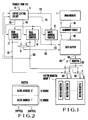
- Fig. 1 is a block diagram showing an arrangement of a data transfer controller according to an embodiment of the present invention;
- Fig. 2 is a memory map showing block assignment of a
data buffer 3 shown in Fig. 1; - Fig. 3 is a block diagram showing a detailed arrangement of a
buffer control circuit 11 shown in Fig. 1; - Fig. 4 is a truth table showing the logic of a read
start designation circuit 209 shown in Fig. 3; and - Fig. 5 is a timing chart showing an operation of the data transfer controller.
- The present invention will be described in detail with reference to the accompanying drawings.
- Fig. 1 shows a data transfer controller according to an embodiment of the present invention. Referring to Fig. 1, a
main memory 1 can read out 16-byte data every clock cycle, and the readout data is supplied to adata buffer 3 through analignment circuit 2. In thedata buffer 3, as shown in Fig. 2, two data each consisting of 16 bytes x 32 words are set in two blocks, respectively. One vector data is set in each block. Two 8-byte elements correspond to one word of thedata buffer 3. - A write address for the
data buffer 3 is supplied from awrite address counter 12 through aline 114. One of values obtained by omitting LSBs (Least Significant Bits) from values ofread address counters switching circuit 15, and the selected value is supplied as a read address through aline 122. - Of the data read out from the
data buffer 3, the upper 8-byte data is supplied to switchingcircuits 5 and 6 through aline 103. The lower 8-byte data is delayed by aregister 4 by one clock cycle, and the delayed data is supplied to theswitching circuits 5 and 6 through aline 105. Theswitching circuits 5 and 6 select elements from the upper and lower 8-byte data corresponding to the same word of thedata buffer 3, and the selected elements are supplied to avector register group 7. This selection is performed by the LSBs of the outputs from theread address counters line 105 are selected when the LSBs are both set at logic "1". - The
vector register group 7 comprises at least two vector registers each for storing vector data having at least one element. The number of vector registers is not important in the present invention, and a description concerning the number of vector registers will be omitted. - The
write address counter 12 is a 6-bit counter for storing a write address for thedata buffer 3. Aninitial address 112 is set in response to a writestart designation signal 113 supplied from abuffer control circuit 11 and is incremented by one every clock cycle. - The
read address counters data buffer 3 to supply the readout vector data to thevector register group 7 throughlines address counter 12 is set in the MSBs of thecounters start designation signals buffer control circuit 11. The remaining bits of thecounters read address counters switching circuit 15, and the selected data is supplied to thedata buffer 3. - The
switching circuit 15 is selected by the LSB of theread address counter 13. When the content of theread address counter 13 represents an even number, theread address counter 13 is selected by theswitching circuit 15. However, when the content of theread address counter 13 represents an odd number, theread address counter 14 is selected by theswitching circuit 15. The LSBs of theaddress counters switching circuits 5 and 6, respectively. - The
buffer control circuit 11 is a circuit for controlling read/write access of thedata buffer 3, and its detailed block diagram is shown in Fig. 3. - Referring to Fig. 3, when a write designation signal constituting request information is supplied to the
buffer control circuit 11 through a line 111-1 and a write element count constituting the request information is supplied to thebuffer control circuit 11 through a line 111-2, a flip-flop 201 and aregister 202 are set. Upon setting of the flip-flop 201, a value of a flip-flop 204 which holds a block address for thedata buffer 3 is inverted. Blocks different in units of write cycles of the data buffer are assigned. The block address held by the flip-flop 204 is set in thewrite address counter 12 by the flip-flop 201. In addition, the content of the flip-flop 201 is supplied to a readstart designation circuit 209 through aline 113. This content is delayed by a flip-flop 203 by one clock cycle, and the delayed data is supplied to the readstart designation circuit 209 through aline 302. - Fig. 4 shows the truth table showing the logic of the read
start designation circuit 209. - Flip-
flops data buffer 3 is being accessed by theread address counters flops start designation signals remaining element counters - The element count held in the
register 202 by the readstart designation signals remaining element counters flops counters - The LSBs of the
read address counters start designation circuit 209 throughlines - The read start designation signal is delayed by flip-
flops lines read address counters - In this embodiment, only 16-byte data is written in the
data buffer 3 every clock cycle. This write access does not limit the scope of the present invention. If a technique disclosed in JP-A- 59-205645 is used, it is apparent to those skilled in the art that read start designation can be performed regardless of write access of thedata buffer 3. - With the above arrangement, an operation of this embodiment will be described with reference to a timing chart of Fig. 5.
- When a write designation signal and a write element count are sent through the
line 111 one clock cycle prior to time T0, the flip-flop 201 is set, and the write element count is set in theregister 202. In this embodiment, the number of elements is set to be 10. - When the flip-
flop 201 is set, theline 113 is set at logic "1" at time T0. A block address of logic "0" and an intrablock address of logic "0" supplied through aline 112 are set in thewrite address counter 12. That is, the count of the write address counter has been set to "0" at time T1. Write access of eight elements is performed from time T1 for 16 bytes every clock cycle, i.e., every two elements for five consecutive clock cycles. - If read access of the
data buffer 3 is not performed by the read address counters 13 and 14 at time T0, the flip-flops line 309 is set at logic "1" by the logic shown in Fig. 4. In this case, the flip-flop 210 is set. The block address of logic "0" stored in the readaddress counter 12 at time T1 is set in the readaddress counter 13 at time T1. At the same time, the intrablock address is cleared to "0". - The read
address counter 13 is set to "0" at time T2 and is then incremented every clock cycle. When the content of the readaddress counter 13 represents an even number, the address signal is supplied to thedata buffer 3. More specifically, 6-bit data except for the LSBs are supplied to thedata buffer 3 at times T2, T4, T6, T8, and T10 to read out data stored ataddresses data buffer 3, respectively. - The LSB of the read
address counter 13 is supplied to theswitching circuit 5. When the content of theaddress counter 13 represents an even number, i.e., when the LSB of theaddress counter 13 is set at logic "0", the upper eight bytes supplied through theline 103 are selected. When content of theaddress counter 13 represents an odd number, i.e., when the LSB is set at logic "1", the lower eight bytes delayed by one clock cycle and supplied through theline 105 are selected. 8-byte data are transferred to thevector register group 7 from time T2 every clock cycle for 10 consecutive clock cycles. That is, 10 elements are continuously transferred to thevector register group 7. - In fact, timings at which the content of the read
address counter 13 represents an even number are times T2, T4, T6, T8, and T10. The upper 8-byte data of the 16-byte data read out from thedata buffer 3 at each of these timings is selected by the switchingcircuit 5. The lower 8-byte data is set in theregister 4. In the next clock cycle, i.e., at each of times T3, T5, T7, T9, and T11, the lower 8-byte data of the 16-byte data read out from thedata buffer 3 at a corresponding one of times T2, T4, T6, T8, and T10 is selected by the switchingcircuit 5. As a result, 8-byte data, i.e., each element is supplied from thedata buffer 3 to thevector register group 7 through theline 106 every clock cycle. - The write access of the
data buffer 3 is completed within five cycles. Write access of the next data is started five or more clock cycles after the write access of the preceding data. For example, when write designation of the next data is detected through theline 111 five clock cycles after write access of the preceding data, an initial address setup designation signal is output to thewrite address counter 12 through theline 113 at time T5 with a delay of one clock cycle by the flip-flop 201. - The value of the flip-
flop 204 is inverted to logic "1" at time T0. At time T5, this value is supplied as a block address to thewrite address counter 12 through theline 112. The write intrablock address is cleared to "0" through theline 112. Therefore, the 6-bitwrite address counter 12 is set to be "32" at time T6 and is then incremented every clock cycle, thereby supplying the write address to thedata buffer 3. - At time T5 the read
address counter 13 is kept operated and the flip-flop 205 is set at logic "1". However, since the readaddress counter 14 is not used, the flip-flop 207 is kept at logic "0". The value of the readaddress counter 13 is "3", and the LSB of logic "1" is supplied to the readstart designation circuit 209. The read start designation signal is output in accordance with the logic of Fig. 4. The read start designation signal is delayed by the flip-flop 211 by one clock cycle, and initial address set designation is performed through theline 118. - Since the block address of the
write address counter 12 is set at logic "1" at time T6, the block address of logic "1" and the intrablock address of logic "0", i.e., "64" are set in the readaddress counter 14. Subsequently, the readaddress counter 14 is incremented every clock cycle in the same manner as in read access of the preceding data. When the content of the readaddress counter 13 represents an odd number, i.e., at times T7, T9, T11,..., the address signal is supplied from the readaddress counter 14 to thedata buffer 3 to access thedata buffer 3. The 16-byte data is read out from thedata buffer 3 at every one of these timings. Since the value of the readaddress counter 14 is always an even number such as 64, 66, 68,..., at these timings, the upper 8-byte data of the data read out from thedata buffer 3 is selected by the switching circuit 6. The lower 8-byte data of the data read out at each of times T7, T9, T11,... is selected at the next timings, i.e., each of times T8, T10, T12,.... The selected data is supplied to thevector register group 7 through theline 107. - Two data are simultaneously supplied to the
vector register group 7 through thelines data buffer 3 to thevector register group 7 through thelines - According to the present invention as has been described above, the data buffer (storing means) and a path for simultaneously transferring a plurality of vector data from the data buffer to the vector register group are arranged between the main memory (first device) and the vector register group (second device). The vector data can be supplied to the vector registers at high speed with simple control. In addition, transfer of the second vector data can be started without waiting for the end of transfer of the first vector data. Therefore, the start of vector calculations can be performed earlier.
Claims (1)
- A data transfer controller for controlling transfer of vector data from a first device (1) to a second device (7), the vector data consisting of a plurality of elements, comprisinga) storing means (3), located between said first and second devices (1 and 7, respectively), for storing the vector data sequentially supplied from said first device (1);b) n read control means (13,14) for controlling to sequentially transfer the vector data from said first device (1) to said storing means (3) and each for controlling to read out one vector data from said storing means (3) to said second device (7);c) n data transfer paths (106,107) respectively corresponding to said n read control means and arranged between said storing means and said second device;d) means (4) for delaying (n-1) elements out of n elements simultaneously read out from the storing means (3) by (n-1) clock cycles corresponding to the numbers of delayed elements; ande) n switching means (5,6) corresponding to the n data transfer paths (106,107) for switching the data delayed (105) by the delay means (4) and the data directly (103) read out from said storing means (3).
Applications Claiming Priority (2)
| Application Number | Priority Date | Filing Date | Title |
|---|---|---|---|
| JP63252902A JPH0792779B2 (en) | 1988-10-08 | 1988-10-08 | Data transfer controller |
| JP252902/88 | 1988-10-08 |
Publications (3)
| Publication Number | Publication Date |
|---|---|
| EP0367995A2 EP0367995A2 (en) | 1990-05-16 |
| EP0367995A3 EP0367995A3 (en) | 1990-12-05 |
| EP0367995B1 true EP0367995B1 (en) | 1995-08-30 |
Family
ID=17243763
Family Applications (1)
| Application Number | Title | Priority Date | Filing Date |
|---|---|---|---|
| EP89118534A Expired - Lifetime EP0367995B1 (en) | 1988-10-08 | 1989-10-05 | Vector data transfer controller |
Country Status (5)
| Country | Link |
|---|---|
| US (1) | US5201058A (en) |
| EP (1) | EP0367995B1 (en) |
| JP (1) | JPH0792779B2 (en) |
| CA (1) | CA2000145C (en) |
| DE (1) | DE68924041T2 (en) |
Families Citing this family (11)
| Publication number | Priority date | Publication date | Assignee | Title |
|---|---|---|---|---|
| US5842033A (en) * | 1992-06-30 | 1998-11-24 | Discovision Associates | Padding apparatus for passing an arbitrary number of bits through a buffer in a pipeline system |
| US5669013A (en) * | 1993-10-05 | 1997-09-16 | Fujitsu Limited | System for transferring M elements X times and transferring N elements one time for an array that is X*M+N long responsive to vector type instructions |
| US5689653A (en) * | 1995-02-06 | 1997-11-18 | Hewlett-Packard Company | Vector memory operations |
| WO1998006042A1 (en) * | 1996-08-07 | 1998-02-12 | Sun Microsystems, Inc. | Wide instruction unpack method and apparatus |
| US5889985A (en) * | 1996-08-07 | 1999-03-30 | Elbrus International | Array prefetch apparatus and method |
| US5961628A (en) * | 1997-01-28 | 1999-10-05 | Samsung Electronics Co., Ltd. | Load and store unit for a vector processor |
| US6665749B1 (en) * | 1999-08-17 | 2003-12-16 | Nec Electronics, Inc. | Bus protocol for efficiently transferring vector data |
| US6591361B1 (en) | 1999-12-28 | 2003-07-08 | International Business Machines Corporation | Method and apparatus for converting data into different ordinal types |
| US6857061B1 (en) | 2000-04-07 | 2005-02-15 | Nintendo Co., Ltd. | Method and apparatus for obtaining a scalar value directly from a vector register |
| US6701424B1 (en) * | 2000-04-07 | 2004-03-02 | Nintendo Co., Ltd. | Method and apparatus for efficient loading and storing of vectors |
| JP3855270B2 (en) * | 2003-05-29 | 2006-12-06 | ソニー株式会社 | Antenna mounting method |
Family Cites Families (14)
| Publication number | Priority date | Publication date | Assignee | Title |
|---|---|---|---|---|
| US4128880A (en) * | 1976-06-30 | 1978-12-05 | Cray Research, Inc. | Computer vector register processing |
| US4166289A (en) * | 1977-09-13 | 1979-08-28 | Westinghouse Electric Corp. | Storage controller for a digital signal processing system |
| JPS6042984B2 (en) * | 1979-12-21 | 1985-09-26 | 富士通株式会社 | pipeline arithmetic unit |
| JPS6042985B2 (en) * | 1979-12-21 | 1985-09-26 | 富士通株式会社 | Parallel execution control method for linked instructions |
| JPS5757372A (en) * | 1980-09-22 | 1982-04-06 | Fujitsu Ltd | Pipeline operating device |
| US4438493A (en) * | 1981-07-06 | 1984-03-20 | Honeywell Information Systems Inc. | Multiwork memory data storage and addressing technique and apparatus |
| JPS58144272A (en) * | 1982-02-19 | 1983-08-27 | Sony Corp | Digital signal processor |
| US4717912A (en) * | 1982-10-07 | 1988-01-05 | Advanced Micro Devices, Inc. | Apparatus for producing any one of a plurality of signals at a single output |
| JPS5975365A (en) * | 1982-10-22 | 1984-04-28 | Hitachi Ltd | Vector processing device |
| JPS6027984A (en) * | 1983-07-27 | 1985-02-13 | Hitachi Ltd | Data processor |
| JPS60134974A (en) * | 1983-12-23 | 1985-07-18 | Hitachi Ltd | Vector processor |
| JPS621067A (en) * | 1985-02-25 | 1987-01-07 | Hitachi Ltd | Vector processor |
| US4760518A (en) * | 1986-02-28 | 1988-07-26 | Scientific Computer Systems Corporation | Bi-directional databus system for supporting superposition of vector and scalar operations in a computer |
| JPH0731669B2 (en) * | 1986-04-04 | 1995-04-10 | 株式会社日立製作所 | Vector processor |
-
1988
- 1988-10-08 JP JP63252902A patent/JPH0792779B2/en not_active Expired - Lifetime
-
1989
- 1989-10-04 CA CA002000145A patent/CA2000145C/en not_active Expired - Fee Related
- 1989-10-05 EP EP89118534A patent/EP0367995B1/en not_active Expired - Lifetime
- 1989-10-05 DE DE68924041T patent/DE68924041T2/en not_active Expired - Fee Related
- 1989-10-06 US US07/418,215 patent/US5201058A/en not_active Expired - Fee Related
Also Published As
| Publication number | Publication date |
|---|---|
| US5201058A (en) | 1993-04-06 |
| JPH0792779B2 (en) | 1995-10-09 |
| DE68924041T2 (en) | 1996-01-25 |
| JPH02100737A (en) | 1990-04-12 |
| CA2000145A1 (en) | 1990-04-08 |
| CA2000145C (en) | 1996-10-29 |
| EP0367995A3 (en) | 1990-12-05 |
| DE68924041D1 (en) | 1995-10-05 |
| EP0367995A2 (en) | 1990-05-16 |
Similar Documents
| Publication | Publication Date | Title |
|---|---|---|
| US5371877A (en) | Apparatus for alternatively accessing single port random access memories to implement dual port first-in first-out memory | |
| EP0263924B1 (en) | On-chip bit reordering structure | |
| US3781812A (en) | Addressing system responsive to a transfer vector for accessing a memory | |
| US5440523A (en) | Multiple-port shared memory interface and associated method | |
| EP0424618A2 (en) | Input/output system | |
| EP0248906A1 (en) | Multi-port memory system | |
| JPH0622034B2 (en) | Multiport vector register file | |
| KR880001171B1 (en) | Sequential word aligned addressing apparatus | |
| EP0367995B1 (en) | Vector data transfer controller | |
| EP0166309A2 (en) | Memory chip for a hierarchical memory system | |
| US4371949A (en) | Time-shared, multi-phase memory accessing system having automatically updatable error logging means | |
| US4174537A (en) | Time-shared, multi-phase memory accessing system having automatically updatable error logging means | |
| US3771142A (en) | Digital data storage system | |
| JPH01182992A (en) | Semiconductor memory device | |
| JPH0531176B2 (en) | ||
| EP0520425B1 (en) | Semiconductor memory device | |
| US6393515B1 (en) | Multi-stream associative memory architecture for computer telephony | |
| US4992979A (en) | Memory structure for nonsequential storage of block bytes in multi bit chips | |
| US5708839A (en) | Method and apparatus for providing bus protocol simulation | |
| EP0057096A2 (en) | Information processing unit | |
| EP0081358B1 (en) | Data processing system providing improved data transfer between modules | |
| US4528648A (en) | Memory management system | |
| US4234918A (en) | Time-shared, multi-phase memory system with error checking and data correcting | |
| US5506747A (en) | Provision of FIFO buffer in RAM | |
| WO1989008293A1 (en) | Bit blitter with narrow shift register |
Legal Events
| Date | Code | Title | Description |
|---|---|---|---|
| PUAI | Public reference made under article 153(3) epc to a published international application that has entered the european phase |
Free format text: ORIGINAL CODE: 0009012 |
|
| 17P | Request for examination filed |
Effective date: 19891026 |
|
| AK | Designated contracting states |
Kind code of ref document: A2 Designated state(s): BE DE FR GB IT NL |
|
| PUAL | Search report despatched |
Free format text: ORIGINAL CODE: 0009013 |
|
| AK | Designated contracting states |
Kind code of ref document: A3 Designated state(s): BE DE FR GB IT NL |
|
| 17Q | First examination report despatched |
Effective date: 19930812 |
|
| GRAA | (expected) grant |
Free format text: ORIGINAL CODE: 0009210 |
|
| AK | Designated contracting states |
Kind code of ref document: B1 Designated state(s): BE DE FR GB IT NL |
|
| REF | Corresponds to: |
Ref document number: 68924041 Country of ref document: DE Date of ref document: 19951005 |
|
| ITF | It: translation for a ep patent filed |
Owner name: MODIANO & ASSOCIATI S.R.L. |
|
| ET | Fr: translation filed | ||
| PLBE | No opposition filed within time limit |
Free format text: ORIGINAL CODE: 0009261 |
|
| STAA | Information on the status of an ep patent application or granted ep patent |
Free format text: STATUS: NO OPPOSITION FILED WITHIN TIME LIMIT |
|
| 26N | No opposition filed | ||
| PGFP | Annual fee paid to national office [announced via postgrant information from national office to epo] |
Ref country code: GB Payment date: 19981009 Year of fee payment: 10 |
|
| PGFP | Annual fee paid to national office [announced via postgrant information from national office to epo] |
Ref country code: FR Payment date: 19981030 Year of fee payment: 10 |
|
| PGFP | Annual fee paid to national office [announced via postgrant information from national office to epo] |
Ref country code: NL Payment date: 19981031 Year of fee payment: 10 |
|
| PGFP | Annual fee paid to national office [announced via postgrant information from national office to epo] |
Ref country code: DE Payment date: 19981229 Year of fee payment: 10 |
|
| PGFP | Annual fee paid to national office [announced via postgrant information from national office to epo] |
Ref country code: BE Payment date: 19990816 Year of fee payment: 11 |
|
| PG25 | Lapsed in a contracting state [announced via postgrant information from national office to epo] |
Ref country code: GB Free format text: LAPSE BECAUSE OF NON-PAYMENT OF DUE FEES Effective date: 19991005 |
|
| PG25 | Lapsed in a contracting state [announced via postgrant information from national office to epo] |
Ref country code: NL Free format text: LAPSE BECAUSE OF NON-PAYMENT OF DUE FEES Effective date: 20000501 |
|
| GBPC | Gb: european patent ceased through non-payment of renewal fee |
Effective date: 19991005 |
|
| PG25 | Lapsed in a contracting state [announced via postgrant information from national office to epo] |
Ref country code: FR Free format text: LAPSE BECAUSE OF NON-PAYMENT OF DUE FEES Effective date: 20000630 |
|
| NLV4 | Nl: lapsed or anulled due to non-payment of the annual fee |
Effective date: 20000501 |
|
| PG25 | Lapsed in a contracting state [announced via postgrant information from national office to epo] |
Ref country code: DE Free format text: LAPSE BECAUSE OF NON-PAYMENT OF DUE FEES Effective date: 20000801 |
|
| REG | Reference to a national code |
Ref country code: FR Ref legal event code: ST |
|
| PG25 | Lapsed in a contracting state [announced via postgrant information from national office to epo] |
Ref country code: BE Free format text: LAPSE BECAUSE OF NON-PAYMENT OF DUE FEES Effective date: 20001031 |
|
| BERE | Be: lapsed |
Owner name: NEC CORP. Effective date: 20001031 |
|
| PG25 | Lapsed in a contracting state [announced via postgrant information from national office to epo] |
Ref country code: IT Free format text: LAPSE BECAUSE OF NON-PAYMENT OF DUE FEES;WARNING: LAPSES OF ITALIAN PATENTS WITH EFFECTIVE DATE BEFORE 2007 MAY HAVE OCCURRED AT ANY TIME BEFORE 2007. THE CORRECT EFFECTIVE DATE MAY BE DIFFERENT FROM THE ONE RECORDED. Effective date: 20051005 |