EP0366324A2 - Efficient cache write technique through deferred tag modification - Google Patents
Efficient cache write technique through deferred tag modification Download PDFInfo
- Publication number
- EP0366324A2 EP0366324A2 EP89310611A EP89310611A EP0366324A2 EP 0366324 A2 EP0366324 A2 EP 0366324A2 EP 89310611 A EP89310611 A EP 89310611A EP 89310611 A EP89310611 A EP 89310611A EP 0366324 A2 EP0366324 A2 EP 0366324A2
- Authority
- EP
- European Patent Office
- Prior art keywords
- cache
- tag
- data
- cycle
- write
- Prior art date
- Legal status (The legal status is an assumption and is not a legal conclusion. Google has not performed a legal analysis and makes no representation as to the accuracy of the status listed.)
- Withdrawn
Links
Images


Classifications
-
- G—PHYSICS
- G06—COMPUTING; CALCULATING OR COUNTING
- G06F—ELECTRIC DIGITAL DATA PROCESSING
- G06F12/00—Accessing, addressing or allocating within memory systems or architectures
- G06F12/02—Addressing or allocation; Relocation
- G06F12/08—Addressing or allocation; Relocation in hierarchically structured memory systems, e.g. virtual memory systems
- G06F12/0802—Addressing of a memory level in which the access to the desired data or data block requires associative addressing means, e.g. caches
- G06F12/0844—Multiple simultaneous or quasi-simultaneous cache accessing
- G06F12/0855—Overlapped cache accessing, e.g. pipeline
Definitions
- This invention relates to digital computer systems which incorporate data caching methods and apparatus.
- DRAM dynamic random access memories
- Caches are small (when compared to the size of the primary storage), fast localized memory arrays which supply data at rates which do not impede the associated processor's performance.
- the viability of caches are based on the probabilities that programs tend to reference a particular piece of data many times before moving onto another (temporal locality), and that successive references made tend to be relatively close to the previous reference made (spatial locality). Cache designers capitalize on this by using the knowledge of the recent past (i.e., previous data reference patterns) to predict the near future in that they collect data relating to references made recently for subsequent use.
- every cache reference made must be validated. Every cache entry must have associated with it a "tag” which describes which data in main memory is currently being represented by it and a “valid” bit which indicates the validity of the cache entry itself.
- a "cache hit” occurs when the desired data resides in the cache while a “cache miss” occurs when it is not.
- the actual transfer of data between the processor and the cache is often conditioned by the results of the cache tag lookup. This tends to increase effective cache access times which often leads to a proportional increased processor cycle times or system performance degradation.
- Minimizing cache store latency is particularly challenging in that the processor must often stall until the cache access is validated since it is the source of the data. Additionally, all cache data modifications must be reflected in the state of the cache tag to maintain cache consistency.
- a common cache store policy is to condition the cache update on the results of the cache tag lookup. When a cache hit occurs, the cache modification may then proceed. If a cache miss occurs, one of two actions may take place, cache write bypass or cache write allocation. Cache write bypass is not a general solution since this is not usable for virtual cache designs, but it does achieve single cycle cache access since no cache modification takes place. Simple cache write allocation would take two cache cycles: cache tag read and cache data/tag write. The serialization of the cache tag lookup to cache data modify increases the effective cache store access time by a factor of two, one cache tag read and one cache data and optionally tag write cycle. Since the processor is the source of the data, it must often stall until the cache tag check is completed.
- the referred cache tag modification provides a simple, efficient, low- overhead cache write technique having a two-stage, overlapped, cache split-cycle access pipeline, which updates the data store in the first or ACC stage and defers any tag store modification until the state of the cache tag check was known. Since the processor is capable of issuing byte writes, a "valid" bit per byte of cache width is employed. If a write-hit is detected, no tag modification is necessary and the processor again has the "illusion" of a single cycle cache access. If the tag matches but the proper valid bits are not set, the cache management function "schedules" a cache tag update for the cycle following the second or EXC stage of the write that missed.
- the cache management function is capable of merging the previous tag valid bit state of the cache with the valid bits that will be set as a result of this write operation. Additionally, if there is a write operation in the immediately following cache operation that is addressed to the same cache line, the bytes selected by this store are merged with the tag update state, thereby avoiding a potential back-to-back write miss. If the tag mismatches, the previous tag/valid bit state is discarded and the tag update state is changed and becomes the bytes being selected by the store in its EXC stage concatenated with the appropriate address tag information. If there is a write operation immediately following that is addressed to the same cache line, the bytes selected by this store, in its ACC stage, are merged with the tag update state.
- this cache write update policy is called "write-allocate", meaning space is allocated in the cache on a write-miss.
- the processor need not be stalled since the data had been captured in the cache. Since the cache management function must regain control to service the cache miss, the processor need only stall if it needs to access the cache while the CMF is using it.
- the first cycle of cache access involves transferring the requested cache data from the cache data store 52 to the processor 54. Additionally, the tag is transferred from the cache tag store 56 to the cache management function, in the Memory Management Unit (MMU) 60, which begins the cache tag comparison while other logic within the cache management function checks for non-cache related exceptions.
- MMU Memory Management Unit
- the method and apparatus of the present invention approaches the optimal solution which includes a means that neither destroys cache contents nor stalls the processor while the normal cache access is underway, achieving a single-cycle cache store access without a significant loss in system performance through deferred tag modification.
- Single-cycle cache store access is achieved by allowing the processor to modify cache data while the tag lookup is being performed. If a cache hit occurs, the processor proceeds uninterrupted. If a cache miss occurs, the tag must be modified to reflect the new contents of that cache entry, since the cache was modified before the status of the cache access was known. Tag modification must either result in the invalidation or the allocation of the modified cache entry. To increase cache performance, cache allocation should be adopted since it is always better to allocate data in a cache rather than purge some.
- deferred tag modifications are application dependent; this invention implies no conceptual limit. During short periods of time, programs tend to reference data that is physically close to one another. Given this, it is possible that successive deferred tag modifications may actually affect the same cache entry. If so, the tag modification operations may be "merged", thereby reducing the number of "free" cache cycles needed to update the cache and increasing the effectiveness of the tag modification buffer.
- the primary concepts of this invention allowing single-cycle cache access are: to read/write the data cache data store now and to update the tag store later, if necessary; to defer tag modifications that result from write misses; to idle cache cycles to minimize the probability of processor stalls; to merge cache tag state, deferred tag state, and current reference state to achieve maximum performance.
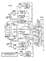
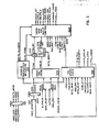
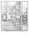
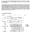
- FIG. 4 A block diagram of a preferred implementation is shown in Fig. 4.
- a processor presents the memory request address to the cache management function (CMF) on the PROC ADDR bus which will then be loaded into the "address register" (AREG), 200, Fig. 4, via the "address mux” (AMUX), 207.
- the request size and type are loaded into the request register, 210.
- the memory request address is presented to the "cache tag store” (CTS), 202.
- CTS cache tag store
- ATM address translation mechanism
- TUQ tag update queue
- the ATM provides the physical address translation on the XLAT_ADDR bus for those systems which use this invention in conjunction with physical caches.
- the ATM provides status which is later used to determine write access privilege. This is the first stage of the cache access pipeline. For write requests the data cache data store is written, unconditionally. The entire cycle is used to check cache and queue hit/miss status.
- the second cycle of cache access, the result of the cache and queue lookup are known and the necessary status is reported back to the processor.
- the TUQ is updated as specified below while the processor proceeds, unaware of the miss condition.
- the processor is stalled until the CMF retrieves the data from memory.
- the CMF' determines the type of request from the signals, WREQ and RREQ.
- the cache data store is written unconditionally, 104.
- the addressed cache tag is compared against the XLAT_ADDR via the "cache tag comparator" (CTC), 203 while byte validity is determined by a matching of cache tag valid bits and the memory reference's BYTE_MASK.
- CTC cache tag comparator
- the TUQ, 206 is queried to determine if the addressed cache entry is scheduled for any subsequent tag modifications, 107.
- a "queue write hit” is said to occur when the cache index matches the queued cache index and the XLAT_ADDR matches the queued cache tag, 110.
- the "cache miss and queue control” (CMQC), 204 determines whether to allocate or invalidate those bytes accessed by this reference. In either case, only the valid bits of the matching queue entry are modified by the TUQ. The pertinent valid bit and control information is presented to the TUQ by the CMCQ over the MISS VALID bus, ALLOCATE, INVALIDATE, and LOAD_Q signals.
- a "queue write miss" is said to occur when the cache index does match any queued cache index or the cache index match exists but the XLAT ADDR does not match that entry's queued cache tag, 110.
- the CMCQ must then "allocate" a new entry in the TUQ.
- the CMCQ is responsible for presenting the proper tag and valid bit information, over the MISS TAG and MISS VALID buses, respectively, to the TUQ. Any valid bit manipulation is done by the CMCQ.
- the allocation/invalidation decision is determined by the state of the WRITE ALLOWED signal.
- the TUQ is instructed, by the CMQC, to merge the BYTE MASK with the current contents to the queued cache valid bits when the ALLOCATE and LOAD_Q signals are asserted and there is a queue write hit, 119.
- the CMF block diagram shows the ATM to be the sole determinant for allowing writes. In general, this need not be the case. In any event, since the cache data store is written before write permission is known, the cache must be invalidated for those cases where writes are not allowed, 118 to avoid cache inconsistencies.
- the CMQC instructs the TUQ to reset the queued valid bits corresponding to those bits that are asserted in the BYTE_MASK by asserting the LOAD_Q and INVALIDATE signals. Merging tag update operations reduce the number of "free" cache cycles needed to update the cache and increase the effectiveness of the TUQ.
- the result of the cache tagivalid bit compare may become important. However, if the write request were not "allowed", a cache invalidation must be scheduled, 111.
- the CMQC passes the previous contents of the cache tag over the MISS TAG bus.
- the CMCQ forms the MISS_VALID bits by resetting the piped cache valid bits corresponding to those bits that were asserted in the BYTE_MASK. This operation effectively "invalidates” those bytes accessed by the illegal cache reference.
- the TUQ is then instructed to load the queue with this information. Since a queue write hit did not occur a new queue entry is created when the CMQC asserts the LOAD Q and INVALIDATE signals, 114, 120.
- a cache allocation is scheduled by creating a new entry in the TUQ which effectively updates the "missing" valid bits.
- the MISS_TAG becomes the piped copy of the XLAT ADDR and MISS VALID is the logical OR of the piped BYTE MASK bits and the piped cache valid bits, 116, 120.
- the TUQ creates this new entry when the LOAD_Q and ALLOCATE signals are asserted.
- the request address would have been presented to the CMF in the same manner as described above for the write requests.
- the data is read from the data store while the queue and tag store lookups are made, 106.
- all queued tag state supercedes any cache tag state when a cache entry has a related valid queue entry in the TUQ (i.e., queued cache index matches cache index of current memory request).
- a "queue read hit" is said to occur when the cache index matches the queued cache index, the XLAT_ADDR matches the queued cache tag, and the BYTE_MASK is inclusive of the queued valid bits. Should a read request result in a queue read hit, then the data read from the cache is valid and the processor can proceed without haste, 108.
- the CMCQ will attempt to only dequeue tag modifications when the cache is not busy, i.e., no memory requests posted, 100 and the queue is not empty, 101.
- the cache tag store is addressed by the queued cache index, Q_CINDEX, via the AREG, 200 via the AMUX, 207.
- the cache tag is updated with the queued cache tag, Q CTAG, and the queued valid bits, Q VALID, TMUX, 200, and VMUX, 208 multiplexors, respectively.
- the queue unload sequence may proceed as long as there are no memory requests pending.
- a long stream of write misses can "fill" the queue before the CMF has a chance to unload anything.
- the CMF will stall the processor and preempt any use of the cache so that an adequate portion of the TUQ can be unloaded, 121.
- the second cycle of cache access involves signalling all cache and non-cache related exception status to the processor 54.
- This latent notification implies the processor must adopt the instruction continue model for trapping data references if the data received in the ACC stage has modified processor state.
- the processor proceeds unaware of the EXC stage of cache access, hence the "illusion" of single cycle cache access.
- Back-to-back cache access is achieved by overlapping the EXC stage of memory reference i with the ACC stage of memory reference i + 1. If the tag mismatches or the tag valid bit is not set, a "cache miss" sequence is triggered. At this time, the cache management function takes control of the cache while the processor waits for the return of the "valid" data to the processor.
- the actual cache read/write takes place during the ACC phase of a data cache access.
- a partial tag comparison is also made in this cycle in the MMU.
- the DTLB is accessed in the ACC cycle and the proper bit set, containing the VA translation (PPN), is selected for comparison with the data cache physical tag.
- the ACC stage reflects the state of the operand reference currently in progress.
- the ACC stage state is composed of the current operand address (CURRENT_EA), current operand size (CURRENT SIZE), and the current cache operation type (CURRENT_OP) and any pending EASRC bus request.
- the source of this information is the EASRC bus, IP_SIZE, and IP_CACHEP OP, and IP_EREQ respectively.
- the MMU can determine the validity of the cache access (i.e. data cache or TB miss, access violation, etc.) in the subsequent cycle. In some cases (e.g. access violations. unaligned address error, translation cache or DTLB miss, force cache miss), faults are detected before the end of the ACC stage, but, signalling is delayed until the EXC stage to maintain a consistent model for trap reporting.
- the MMU Since the MMU is the default master, the MMU will regain control of the EASRC bus in this stage if there are not any pending IP or bus interface EASRC bus requests. If the CURRENT_OP is a STORE the MMU will recirculate the write miss virtual address and prepare the cache tag to be updated. If the CURRENT_OP is a LOAD, the Secondary TB miss address is recirculated and the cache is prepared for a TB lookup. These actions are done so that, probabilistically, the MMU could shave a cycle out of write miss or DTLB miss by assuming one of these two conditions will occur. If a write miss is not detected, the MMU will simply rewrite the tag. If a DTLB miss does not happen, the MMU will ignore the secondary TB tag it fetched.
- EXCEPTION (EXC) stage contains the state of a potentially faulting data cache reference.
- the EXC stage state is composed of the missed operand address (MISS_EA), the missed operand size (MISS_SIZE), and the missed cache operation type (MISS OP).
- This pipeline stage is fed directly from the previous pipeline stage, the ACC stage. Additionally, the result of the access check is saved in a register (DCHECK), which includes the CURRENT_EA/MISS) EA comparison result (write, miss merge) and the physical address of the operand accessed is saved in the DPA (data physical address) register.
- DCHECK includes the CURRENT_EA/MISS
- EA comparison result write, miss merge
- the physical address of the operand accessed is saved in the DPA (data physical address) register.
- This stage contains all the necessary information to complete a cache access check, to issue a request to the physical memory/I/O subsystem, if needed, to aid in stall recovery, and to signal any detected exceptions in the IP.
- MMU_EASRC_BUSY in the EXC (invalidates actually can happen in any cycle) stage.
- This type of stall has the effect of stalling any instruction in its EA stage, while any other instruction in its DC or WL stage progress.
- a LOAD(i+1) or STORE(i + 1) could be in its DC phase. It is useful to save the status of that cache access, rather than rerun that reference, after the write miss service, to regain the access state of i + 1. This state makes up the WMM stage.
- a read miss occurs whenever the data cache tag does not match the virtual address translation or when the tag matches but the proper byte valid bits are not set properly. For example, if the IP reads byte 0 of a cache line and all the valid bits for that line, except for byte 0, are set, a miss occurs even if the data cache tag matches the virtual address translation.
- the MMU stalls the requesting processor and its the data cache pipeline, by asserting MMU_EASRC_BUSY and negating MMU_EVALID.
- the MMU then gains control of the EASRC, DATA, DTAG busses in preparation for the subsequent cache allocation.
- the BIF supplies the virtual address of the miss operand by placing it on the physical address bus, enabling the PASRC-to-EASRC bus transceivers and also supplies the necessary cache control for the actual cache allocation.
- a read request for two quadwords is made to the BIF if the missed reference was an integer .LOAD.
- the MMU supplies the physical address of the missed reference with the read request.
- Eight quadwords are fetched if the missed reference was a floating point LOAD on a 64-byte boundary.
- the BUS IC notifies the MMU by placing the code for READ_MISS_DATA_AVAIL on the MEM_RESP control lines and places the requested data on the DATA bus.
- the MMY will also recirculate EASRC(2:0) and IP_SIZE(1:0) of the missed reference, during the allocation process.
- the new data and tag (supplied by the MMU) are written into the cache while the BIF increments the refill address on EASRC by 8. In the next cycle, the BIF writes the second quadword and associated tag into the data cache.
- MMU_EVALID is asserted in the following cycle to indicate to the IP/FP that the requested data is available.
- the MMU conditionally restores the state of the EAREG by testing the CURRENT_OP field in the ACCESS_EA stage of the MMU pipeline. If a cache request was made in the cycle following the cache access that missed, CURRENT_EA, which contains the virtual address of the subsequent cache access, in the ACCESS_EA pipeline is placed on the EASRC bus to be loaded into the EAREG.
- the MMU recirculates IP_CACHE_OP, IP SIZE (for the external control PAL's benefit) of the reference, to restore the memory pipeline.
- the MMU then negates MMU_EVALiO and the IP/FP pipelines continues with valid data.
- the MMU and BIF always exchanges ownership of the EASRC bus when the MMU during the last line of the allocation. If an ECCC error occurs on the last line of the cache allocation, the MMU will give the EASRC bus back to the BIF. The BIF then recirculates the address of the last cache line. Once valid data becomes available, the BIF must hold the address, control, and data one additional cycle for the new valid data. If an ECCU or bus error is detected, the BIF again holds the address, control, and data for additional cycle and the MMU will invalidate the bad line in the second cycle the address is held.
Landscapes
- Engineering & Computer Science (AREA)
- Theoretical Computer Science (AREA)
- Physics & Mathematics (AREA)
- General Engineering & Computer Science (AREA)
- General Physics & Mathematics (AREA)
- Memory System Of A Hierarchy Structure (AREA)
- Advance Control (AREA)
Abstract
Description
- This invention relates to digital computer systems which incorporate data caching methods and apparatus.
- Under ideal conditions, increased processor speed translates into an increased demand on memory per unit time. Processing elements often are capable of operating at rates that exceed those of dynamic random access memories (DRAM) which are most often used for primary storage. When system performance is paramount, an additional level of memory hierarchy, called a cache", whose performance is matched to that of the associated processor is incorporated.
- Caches are small (when compared to the size of the primary storage), fast localized memory arrays which supply data at rates which do not impede the associated processor's performance. The viability of caches are based on the probabilities that programs tend to reference a particular piece of data many times before moving onto another (temporal locality), and that successive references made tend to be relatively close to the previous reference made (spatial locality). Cache designers capitalize on this by using the knowledge of the recent past (i.e., previous data reference patterns) to predict the near future in that they collect data relating to references made recently for subsequent use.
- In processing systems which employ data caches, every cache reference made must be validated. Every cache entry must have associated with it a "tag" which describes which data in main memory is currently being represented by it and a "valid" bit which indicates the validity of the cache entry itself. A "cache hit" occurs when the desired data resides in the cache while a "cache miss" occurs when it is not. The actual transfer of data between the processor and the cache is often conditioned by the results of the cache tag lookup. This tends to increase effective cache access times which often leads to a proportional increased processor cycle times or system performance degradation.
- Minimizing cache store latency is particularly challenging in that the processor must often stall until the cache access is validated since it is the source of the data. Additionally, all cache data modifications must be reflected in the state of the cache tag to maintain cache consistency.
- A common cache store policy is to condition the cache update on the results of the cache tag lookup. When a cache hit occurs, the cache modification may then proceed. If a cache miss occurs, one of two actions may take place, cache write bypass or cache write allocation. Cache write bypass is not a general solution since this is not usable for virtual cache designs, but it does achieve single cycle cache access since no cache modification takes place. Simple cache write allocation would take two cache cycles: cache tag read and cache data/tag write. The serialization of the cache tag lookup to cache data modify increases the effective cache store access time by a factor of two, one cache tag read and one cache data and optionally tag write cycle. Since the processor is the source of the data, it must often stall until the cache tag check is completed.
- Another approach which avoids this serialization penalty completely ignores the state of the cache tag. With this approach, every cache store operation bypasses the cache. To maintain cache consistency, the modified cache entry is invalidated without regard. The processor need only supply data for one cache (data) write cycle. This approach reduces the effective store cache access time, but not without significant losses in cache performance since these invalidations may purge useful data from the cache.
- The referred cache tag modification according to the present invention provides a simple, efficient, low- overhead cache write technique having a two-stage, overlapped, cache split-cycle access pipeline, which updates the data store in the first or ACC stage and defers any tag store modification until the state of the cache tag check was known. Since the processor is capable of issuing byte writes, a "valid" bit per byte of cache width is employed. If a write-hit is detected, no tag modification is necessary and the processor again has the "illusion" of a single cycle cache access. If the tag matches but the proper valid bits are not set, the cache management function "schedules" a cache tag update for the cycle following the second or EXC stage of the write that missed.
- The cache management function (CMF) is capable of merging the previous tag valid bit state of the cache with the valid bits that will be set as a result of this write operation. Additionally, if there is a write operation in the immediately following cache operation that is addressed to the same cache line, the bytes selected by this store are merged with the tag update state, thereby avoiding a potential back-to-back write miss. If the tag mismatches, the previous tag/valid bit state is discarded and the tag update state is changed and becomes the bytes being selected by the store in its EXC stage concatenated with the appropriate address tag information. If there is a write operation immediately following that is addressed to the same cache line, the bytes selected by this store, in its ACC stage, are merged with the tag update state. In either case, this cache write update policy is called "write-allocate", meaning space is allocated in the cache on a write-miss. Moreover, during a write-miss sequence, the processor need not be stalled since the data had been captured in the cache. Since the cache management function must regain control to service the cache miss, the processor need only stall if it needs to access the cache while the CMF is using it.
- These'said further features of the present invention are better understood by reading the following detailed description taken together with the drawing, wherein:
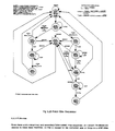
- Fig. 1 is a block diagram of a pipeline processor of incorporating one embodiment of the present invention;
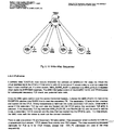
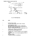
- Fig. 2 is a flow diagram showing the operation according to one embodiment of the present invention; and
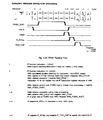
- Fig. 3 is a more detailed block diagram showing specific functional elements operative according to the flow chart of Fig. 2 in the implementation of Fig. 1.
- Further details of one embodiment of the present invention are provided in Appendixes I and II.
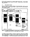
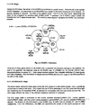
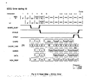
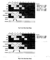
- Referring to the process shown in the block diagram 50 of Fig. 1 for a read operation, the first cycle of cache access, herein called the ACCess (ACC) stage, involves transferring the requested cache data from the
cache data store 52 to theprocessor 54. Additionally, the tag is transferred from thecache tag store 56 to the cache management function, in the Memory Management Unit (MMU) 60, which begins the cache tag comparison while other logic within the cache management function checks for non-cache related exceptions. Further details regarding exceptions are provided in APOLL-115XX, entitled DUPLICATE TAG STORE PURGE QUEUE, and in APOLL-119XX, entitled METHOD AND APPARATUS FOR DRAM MEMORY PERFORMANCE ENHANCEMENT, both filed concurrently herewith and incorporated by reference. By the end of the ACC stage, the data has been clocked into theprocessor 54 and cache tag compare is completed. - The present invention is described with respect to Figs. 2 and 3, wherein:
- The method and apparatus of the present invention approaches the optimal solution which includes a means that neither destroys cache contents nor stalls the processor while the normal cache access is underway, achieving a single-cycle cache store access without a significant loss in system performance through deferred tag modification. Single-cycle cache store access is achieved by allowing the processor to modify cache data while the tag lookup is being performed. If a cache hit occurs, the processor proceeds uninterrupted. If a cache miss occurs, the tag must be modified to reflect the new contents of that cache entry, since the cache was modified before the status of the cache access was known. Tag modification must either result in the invalidation or the allocation of the modified cache entry. To increase cache performance, cache allocation should be adopted since it is always better to allocate data in a cache rather than purge some.
- Typically, programs do not reference data in memory every cycle. This observation implies that there will always be unused cache bandwidth. It is the intention of this invention, through buffering, to defer tag modifications that result from cache write misses, to these "free" cache cycles so that processor stalls may be avoided. Tag modification deferment does imply that the cache is temporarily inconsistent. Subsequent cache accesses, to entries which have pending tag modifications, must validate their accesses against any pending tag updates scheduled in the tag modification buffer as well as the cache itself. Once the buffer is emptied, cache consistency is restored.
- The number of deferred tag modifications is application dependent; this invention implies no conceptual limit. During short periods of time, programs tend to reference data that is physically close to one another. Given this, it is possible that successive deferred tag modifications may actually affect the same cache entry. If so, the tag modification operations may be "merged", thereby reducing the number of "free" cache cycles needed to update the cache and increasing the effectiveness of the tag modification buffer.
- The primary concepts of this invention allowing single-cycle cache access are: to read/write the data cache data store now and to update the tag store later, if necessary; to defer tag modifications that result from write misses; to idle cache cycles to minimize the probability of processor stalls; to merge cache tag state, deferred tag state, and current reference state to achieve maximum performance.
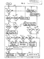
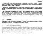
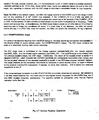
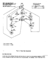
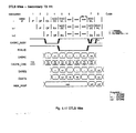
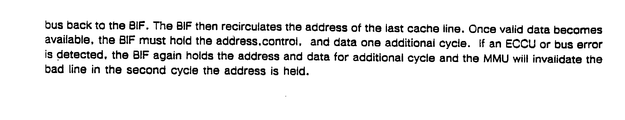
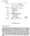
- Although the cache access flow represented in the flow chart of Fig. 3 serializes many tests and activities, actual implementations of this invention will adopt some degree of paralellism to maximize performance. A block diagram of a preferred implementation is shown in Fig. 4. At cycle, t, a processor presents the memory request address to the cache management function (CMF) on the PROC ADDR bus which will then be loaded into the "address register" (AREG), 200, Fig. 4, via the "address mux" (AMUX), 207. The request size and type are loaded into the request register, 210.
- At cycle, t+1, the memory request address is presented to the "cache tag store" (CTS), 202. the "address translation mechanism" (ATM), 201, and the "tag update queue" (TUQ), 206 via the CINDEX bus. The ATM provides the physical address translation on the XLAT_ADDR bus for those systems which use this invention in conjunction with physical caches. In addition, the ATM provides status which is later used to determine write access privilege. This is the first stage of the cache access pipeline. For write requests the data cache data store is written, unconditionally. The entire cycle is used to check cache and queue hit/miss status.
- At cycle, t+2, the second cycle of cache access, the result of the cache and queue lookup are known and the necessary status is reported back to the processor. When a write miss occurred, the TUQ is updated as specified below while the processor proceeds, unaware of the miss condition. When a read miss occurs, the processor is stalled until the CMF retrieves the data from memory.
- When a memory request is made, 100, Fig. 3, the CMF'determine the type of request from the signals, WREQ and RREQ. In the case of a write request, the cache data store is written unconditionally, 104. The addressed cache tag is compared against the XLAT_ADDR via the "cache tag comparator" (CTC), 203 while byte validity is determined by a matching of cache tag valid bits and the memory reference's BYTE_MASK. Simultaneously, the TUQ, 206 is queried to determine if the addressed cache entry is scheduled for any subsequent tag modifications, 107.
- A "queue write hit" is said to occur when the cache index matches the queued cache index and the XLAT_ADDR matches the queued cache tag, 110. The "cache miss and queue control" (CMQC), 204 then determines whether to allocate or invalidate those bytes accessed by this reference. In either case, only the valid bits of the matching queue entry are modified by the TUQ. The pertinent valid bit and control information is presented to the TUQ by the CMCQ over the MISS VALID bus, ALLOCATE, INVALIDATE, and LOAD_Q signals.
- A "queue write miss" is said to occur when the cache index does match any queued cache index or the cache index match exists but the XLAT ADDR does not match that entry's queued cache tag, 110. The CMCQ must then "allocate" a new entry in the TUQ. The CMCQ is responsible for presenting the proper tag and valid bit information, over the MISS TAG and MISS VALID buses, respectively, to the TUQ. Any valid bit manipulation is done by the CMCQ. The allocation/invalidation decision is determined by the state of the WRITE ALLOWED signal. If asserted, 117, the TUQ is instructed, by the CMQC, to merge the BYTE MASK with the current contents to the queued cache valid bits when the ALLOCATE and LOAD_Q signals are asserted and there is a queue write hit, 119.
- There are several reasons for disallowing cache writes: non-resident data, insufficient access privileges, unaligned memory reference, unencacheable data, etc. The CMF block diagram shows the ATM to be the sole determinant for allowing writes. In general, this need not be the case. In any event, since the cache data store is written before write permission is known, the cache must be invalidated for those cases where writes are not allowed, 118 to avoid cache inconsistencies. The CMQC instructs the TUQ to reset the queued valid bits corresponding to those bits that are asserted in the BYTE_MASK by asserting the LOAD_Q and INVALIDATE signals. Merging tag update operations reduce the number of "free" cache cycles needed to update the cache and increase the effectiveness of the TUQ.
- When a queue write hit does not occur, 110, then the result of the cache tagivalid bit compare may become important. However, if the write request were not "allowed", a cache invalidation must be scheduled, 111. The CMQC passes the previous contents of the cache tag over the MISS TAG bus. The CMCQ forms the MISS_VALID bits by resetting the piped cache valid bits corresponding to those bits that were asserted in the BYTE_MASK. This operation effectively "invalidates" those bytes accessed by the illegal cache reference. The TUQ is then instructed to load the queue with this information. Since a queue write hit did not occur a new queue entry is created when the CMQC asserts the LOAD Q and INVALIDATE signals, 114, 120.
- When a queue hit does not occur and the cache write is allowed and the cache tag matches the XLAT_ADDR, then that cache entry is totally unrelated to this cache reference, 112 and a cache allocation is scheduled by creating a new entry in the TUQ. The MISS TAG becomes the piped XLAT ADDR and MISS VALID becomes the pipe BYTE_MASK bits, 115, 120. The TUQ creates this new entry when the LOAD_Q and ALLOCATE signals are asserted.
- When a queue hit does not occur and the cache write is allowed and the cache tag matches the XLAT_ADDR and the valid bits do not match, 113, a cache allocation is scheduled by creating a new entry in the TUQ which effectively updates the "missing" valid bits. The MISS_TAG becomes the piped copy of the XLAT ADDR and MISS VALID is the logical OR of the piped BYTE MASK bits and the piped cache valid bits, 116, 120. The TUQ creates this new entry when the LOAD_Q and ALLOCATE signals are asserted. When a queue hit does not occur and the cache write is allowed and the cache tag matches the XLAT_ADDR and the valid bits match, 113, a cache hit is said to occur. No tag modifications are scheduled.
- Had the originally issued memory reference been a read request, 105, the request address would have been presented to the CMF in the same manner as described above for the write requests. For read requests, the data is read from the data store while the queue and tag store lookups are made, 106. It should be noted that all queued tag state supercedes any cache tag state when a cache entry has a related valid queue entry in the TUQ (i.e., queued cache index matches cache index of current memory request). A "queue read hit" is said to occur when the cache index matches the queued cache index, the XLAT_ADDR matches the queued cache tag, and the BYTE_MASK is inclusive of the queued valid bits. Should a read request result in a queue read hit, then the data read from the cache is valid and the processor can proceed without haste, 108.
- When a read request cannot be satisfied by the TUQ, then the result of the cache tag/valid bit comparison becomes important. If the cache tag matches the XLAT_ADDR and the BYTE_MASK is inclusive of the cache tag valid bits, then a "read hit" is said to occur and the processor can proceed without haste, 109. Otherwise, a "read miss" occurs and the processor must stall until the requested data can be fetched from memory, 103. The steps taken beyond this point are beyond the scope of this invention.
- The CMCQ will attempt to only dequeue tag modifications when the cache is not busy, i.e., no memory requests posted, 100 and the queue is not empty, 101. When this condition exists the CMCQ takes control to the cache. The cache tag store is addressed by the queued cache index, Q_CINDEX, via the AREG, 200 via the AMUX, 207. The cache tag is updated with the queued cache tag, Q CTAG, and the queued valid bits, Q VALID, TMUX, 200, and VMUX, 208 multiplexors, respectively. The queue unload sequence may proceed as long as there are no memory requests pending. For finite length queues, a long stream of write misses can "fill" the queue before the CMF has a chance to unload anything. In this case, the CMF will stall the processor and preempt any use of the cache so that an adequate portion of the TUQ can be unloaded, 121.
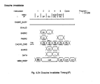
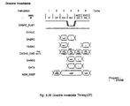
- For a read operation, the second cycle of cache access, herein called the EXCeption (EXC) stage, involves signalling all cache and non-cache related exception status to the
processor 54. This latent notification implies the processor must adopt the instruction continue model for trapping data references if the data received in the ACC stage has modified processor state. In the case where the tag matches and the tag valid bit is set (i.e., "cache hit"), the processor proceeds unaware of the EXC stage of cache access, hence the "illusion" of single cycle cache access. Back-to-back cache access is achieved by overlapping the EXC stage of memory reference i with the ACC stage of memory reference i + 1. If the tag mismatches or the tag valid bit is not set, a "cache miss" sequence is triggered. At this time, the cache management function takes control of the cache while the processor waits for the return of the "valid" data to the processor. - The actual cache read/write takes place during the ACC phase of a data cache access. According to this present invention, a partial tag comparison is also made in this cycle in the MMU. The DTLB is accessed in the ACC cycle and the proper bit set, containing the VA translation (PPN), is selected for comparison with the data cache physical tag. The ACC stage reflects the state of the operand reference currently in progress.
- The ACC stage state is composed of the current operand address (CURRENT_EA), current operand size (CURRENT SIZE), and the current cache operation type (CURRENT_OP) and any pending EASRC bus request. The source of this information is the EASRC bus, IP_SIZE, and IP_CACHEP OP, and IP_EREQ respectively. From this information, the MMU can determine the validity of the cache access (i.e. data cache or TB miss, access violation, etc.) in the subsequent cycle. In some cases (e.g. access violations. unaligned address error, translation cache or DTLB miss, force cache miss), faults are detected before the end of the ACC stage, but, signalling is delayed until the EXC stage to maintain a consistent model for trap reporting.
- Since the MMU is the default master, the MMU will regain control of the EASRC bus in this stage if there are not any pending IP or bus interface EASRC bus requests. If the CURRENT_OP is a STORE the MMU will recirculate the write miss virtual address and prepare the cache tag to be updated. If the CURRENT_OP is a LOAD, the Secondary TB miss address is recirculated and the cache is prepared for a TB lookup. These actions are done so that, probabilistically, the MMU could shave a cycle out of write miss or DTLB miss by assuming one of these two conditions will occur. If a write miss is not detected, the MMU will simply rewrite the tag. If a DTLB miss does not happen, the MMU will ignore the secondary TB tag it fetched.
- Any stalls or exceptions resulting from the DTLB lookup- or the data cache tag comparison are signaled in the second phase of cache access called, the EXCEPTION (EXC) stage. The EXC stage contains the state of a potentially faulting data cache reference.
- The EXC stage state is composed of the missed operand address (MISS_EA), the missed operand size (MISS_SIZE), and the missed cache operation type (MISS OP). This pipeline stage is fed directly from the previous pipeline stage, the ACC stage. Additionally, the result of the access check is saved in a register (DCHECK), which includes the CURRENT_EA/MISS) EA comparison result (write, miss merge) and the physical address of the operand accessed is saved in the DPA (data physical address) register. This stage contains all the necessary information to complete a cache access check, to issue a request to the physical memory/I/O subsystem, if needed, to aid in stall recovery, and to signal any detected exceptions in the IP.
- If the virtual address translation is in the DTLB (DTLB Hit), no access violations are detected, the operand is in the data cache (Dcache Hit), and there are not any higher priority requestor for the EASRC bus, the IP and MMU pipeline progress, undisturbed. The operand transfer is considered valid. Normal Pipeline operation is shown below.

- If a write miss is detected or an invalidate is posted, the MMU will have asserted MMU_EASRC_BUSY in the EXC (invalidates actually can happen in any cycle) stage. This type of stall has the effect of stalling any instruction in its EA stage, while any other instruction in its DC or WL stage progress. At the time the write miss was detected (WL of i), a LOAD(i+1) or STORE(i + 1) could be in its DC phase. It is useful to save the status of that cache access, rather than rerun that reference, after the write miss service, to regain the access state of i + 1. This state makes up the WMM stage.
- A read miss occurs whenever the data cache tag does not match the virtual address translation or when the tag matches but the proper byte valid bits are not set properly. For example, if the IP reads
byte 0 of a cache line and all the valid bits for that line, except forbyte 0, are set, a miss occurs even if the data cache tag matches the virtual address translation. - When one of the above conditions exists, the MMU stalls the requesting processor and its the data cache pipeline, by asserting MMU_EASRC_BUSY and negating MMU_EVALID. The MMU then gains control of the EASRC, DATA, DTAG busses in preparation for the subsequent cache allocation. The BIF supplies the virtual address of the miss operand by placing it on the physical address bus, enabling the PASRC-to-EASRC bus transceivers and also supplies the necessary cache control for the actual cache allocation. A read request for two quadwords is made to the BIF if the missed reference was an integer .LOAD. The MMU supplies the physical address of the missed reference with the read request. Eight quadwords are fetched if the missed reference was a floating point LOAD on a 64-byte boundary. When the data becomes available to the MMU, the BUS IC notifies the MMU by placing the code for READ_MISS_DATA_AVAIL on the MEM_RESP control lines and places the requested data on the DATA bus. The MMY will also recirculate EASRC(2:0) and IP_SIZE(1:0) of the missed reference, during the allocation process. The new data and tag (supplied by the MMU) are written into the cache while the BIF increments the refill address on EASRC by 8. In the next cycle, the BIF writes the second quadword and associated tag into the data cache. As soon as the data requested by the IP/FP comes across the DATA bus, MMU_EVALID is asserted in the following cycle to indicate to the IP/FP that the requested data is available. When cache allocation is complete, the MMU conditionally restores the state of the EAREG by testing the CURRENT_OP field in the ACCESS_EA stage of the MMU pipeline. If a cache request was made in the cycle following the cache access that missed, CURRENT_EA, which contains the virtual address of the subsequent cache access, in the ACCESS_EA pipeline is placed on the EASRC bus to be loaded into the EAREG. Additionally, the MMU recirculates IP_CACHE_OP, IP SIZE (for the external control PAL's benefit) of the reference, to restore the memory pipeline. The MMU then negates MMU_EVALiO and the IP/FP pipelines continues with valid data.
- The MMU and BIF always exchanges ownership of the EASRC bus when the MMU during the last line of the allocation. If an ECCC error occurs on the last line of the cache allocation, the MMU will give the EASRC bus back to the BIF. The BIF then recirculates the address of the last cache line. Once valid data becomes available, the BIF must hold the address, control, and data one additional cycle for the new valid data. If an ECCU or bus error is detected, the BIF again holds the address, control, and data for additional cycle and the MMU will invalidate the bad line in the second cycle the address is held.
Claims (2)
Applications Claiming Priority (2)
| Application Number | Priority Date | Filing Date | Title |
|---|---|---|---|
| US26405888A | 1988-10-28 | 1988-10-28 | |
| US264058 | 1988-10-28 |
Publications (2)
| Publication Number | Publication Date |
|---|---|
| EP0366324A2 true EP0366324A2 (en) | 1990-05-02 |
| EP0366324A3 EP0366324A3 (en) | 1991-09-18 |
Family
ID=23004384
Family Applications (1)
| Application Number | Title | Priority Date | Filing Date |
|---|---|---|---|
| EP19890310611 Withdrawn EP0366324A3 (en) | 1988-10-28 | 1989-10-16 | Efficient cache write technique through deferred tag modification |
Country Status (2)
| Country | Link |
|---|---|
| EP (1) | EP0366324A3 (en) |
| JP (1) | JP3219196B2 (en) |
Families Citing this family (1)
| Publication number | Priority date | Publication date | Assignee | Title |
|---|---|---|---|---|
| US6950906B2 (en) * | 2002-12-13 | 2005-09-27 | Hewlett-Packard Development Company, L.P. | System for and method of operating a cache |
Citations (1)
| Publication number | Priority date | Publication date | Assignee | Title |
|---|---|---|---|---|
| JPS63206843A (en) * | 1987-02-24 | 1988-08-26 | Matsushita Electric Ind Co Ltd | Cache memory device |
-
1989
- 1989-10-16 EP EP19890310611 patent/EP0366324A3/en not_active Withdrawn
- 1989-10-27 JP JP28158689A patent/JP3219196B2/en not_active Expired - Fee Related
Patent Citations (1)
| Publication number | Priority date | Publication date | Assignee | Title |
|---|---|---|---|---|
| JPS63206843A (en) * | 1987-02-24 | 1988-08-26 | Matsushita Electric Ind Co Ltd | Cache memory device |
Non-Patent Citations (1)
| Title |
|---|
| PATENT ABSTRACTS OF JAPAN vol. 12, no. 497 (P-806)December 26, 1988 & JP-A-63 206 843 (MATSUSHITA ELECTRIC IND. CO. LTD. ) August 26, 1988 * |
Also Published As
| Publication number | Publication date |
|---|---|
| JP3219196B2 (en) | 2001-10-15 |
| EP0366324A3 (en) | 1991-09-18 |
| JPH02224042A (en) | 1990-09-06 |
Similar Documents
| Publication | Publication Date | Title |
|---|---|---|
| US5163142A (en) | Efficient cache write technique through deferred tag modification | |
| US11803486B2 (en) | Write merging on stores with different privilege levels | |
| US6725337B1 (en) | Method and system for speculatively invalidating lines in a cache | |
| US8782348B2 (en) | Microprocessor cache line evict array | |
| US6473837B1 (en) | Snoop resynchronization mechanism to preserve read ordering | |
| US10613792B2 (en) | Efficient enforcement of barriers with respect to memory move sequences | |
| US10572179B2 (en) | Speculatively performing memory move requests with respect to a barrier | |
| US6473832B1 (en) | Load/store unit having pre-cache and post-cache queues for low latency load memory operations | |
| US10140052B2 (en) | Memory access in a data processing system utilizing copy and paste instructions | |
| US10152322B2 (en) | Memory move instruction sequence including a stream of copy-type and paste-type instructions | |
| US10241945B2 (en) | Memory move supporting speculative acquisition of source and destination data granules including copy-type and paste-type instructions | |
| US10346164B2 (en) | Memory move instruction sequence targeting an accelerator switchboard | |
| US10126952B2 (en) | Memory move instruction sequence targeting a memory-mapped device | |
| US10331373B2 (en) | Migration of memory move instruction sequences between hardware threads | |
| US9996298B2 (en) | Memory move instruction sequence enabling software control | |
| US20070022250A1 (en) | System and method of responding to a cache read error with a temporary cache directory column delete | |
| EP0366324A2 (en) | Efficient cache write technique through deferred tag modification | |
| US7035981B1 (en) | Asynchronous input/output cache having reduced latency |
Legal Events
| Date | Code | Title | Description |
|---|---|---|---|
| PUAI | Public reference made under article 153(3) epc to a published international application that has entered the european phase |
Free format text: ORIGINAL CODE: 0009012 |
|
| AK | Designated contracting states |
Kind code of ref document: A2 Designated state(s): AT BE CH DE ES FR GB GR IT LI LU NL SE |
|
| RBV | Designated contracting states (corrected) |
Designated state(s): DE FR GB |
|
| PUAL | Search report despatched |
Free format text: ORIGINAL CODE: 0009013 |
|
| AK | Designated contracting states |
Kind code of ref document: A3 Designated state(s): AT BE CH DE ES FR GB GR IT LI LU NL SE |
|
| 17P | Request for examination filed |
Effective date: 19920127 |
|
| RAP1 | Party data changed (applicant data changed or rights of an application transferred) |
Owner name: HEWLETT-PACKARD COMPANY |
|
| 17Q | First examination report despatched |
Effective date: 19950405 |
|
| GRAG | Despatch of communication of intention to grant |
Free format text: ORIGINAL CODE: EPIDOS AGRA |
|
| GRAH | Despatch of communication of intention to grant a patent |
Free format text: ORIGINAL CODE: EPIDOS IGRA |
|
| STAA | Information on the status of an ep patent application or granted ep patent |
Free format text: STATUS: THE APPLICATION IS DEEMED TO BE WITHDRAWN |
|
| 18D | Application deemed to be withdrawn |
Effective date: 19961119 |