EP0366243A2 - Combined optical power meter and receiver - Google Patents
Combined optical power meter and receiver Download PDFInfo
- Publication number
- EP0366243A2 EP0366243A2 EP89309080A EP89309080A EP0366243A2 EP 0366243 A2 EP0366243 A2 EP 0366243A2 EP 89309080 A EP89309080 A EP 89309080A EP 89309080 A EP89309080 A EP 89309080A EP 0366243 A2 EP0366243 A2 EP 0366243A2
- Authority
- EP
- European Patent Office
- Prior art keywords
- photodiode
- optical power
- power meter
- current
- receiver
- Prior art date
- Legal status (The legal status is an assumption and is not a legal conclusion. Google has not performed a legal analysis and makes no representation as to the accuracy of the status listed.)
- Withdrawn
Links
- 230000003287 optical effect Effects 0.000 title claims abstract description 55
- 239000003990 capacitor Substances 0.000 claims description 6
- 230000035945 sensitivity Effects 0.000 abstract description 12
- 230000007423 decrease Effects 0.000 abstract description 4
- 238000010586 diagram Methods 0.000 description 3
- 230000003292 diminished effect Effects 0.000 description 2
- 230000000694 effects Effects 0.000 description 2
- 230000008878 coupling Effects 0.000 description 1
- 238000010168 coupling process Methods 0.000 description 1
- 238000005859 coupling reaction Methods 0.000 description 1
- 230000000717 retained effect Effects 0.000 description 1
Images
Classifications
-
- H—ELECTRICITY
- H04—ELECTRIC COMMUNICATION TECHNIQUE
- H04B—TRANSMISSION
- H04B10/00—Transmission systems employing electromagnetic waves other than radio-waves, e.g. infrared, visible or ultraviolet light, or employing corpuscular radiation, e.g. quantum communication
- H04B10/60—Receivers
- H04B10/66—Non-coherent receivers, e.g. using direct detection
- H04B10/69—Electrical arrangements in the receiver
- H04B10/697—Arrangements for reducing noise and distortion
Definitions
- This invention relates to optical power meters and optical receivers and more particularly to optical power meters and receivers which are combined for simultaneous operation.
- optical power meters use a single photodiode in combination with an integrating transimpedance amplifier to provide an output voltage which is representative of the average input optical power. Such optical power meters are characterized by high sensitivity and low bandwidth.
- most prior art optical receivers use a single photodiode in combination with a transimpedance amplifier to provide a voltage output which is representative of the instantaneous current through the photodiode. Such optical receivers are characterized by lower sensitivity and high bandwidth.
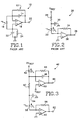
- FIG. 1 A prior art optical power meter is shown in FIG. 1.
- the optical power meter 10 consists of an operational amplifier 18 in which resistors 12 and 24 form current summing inputs at the positive and negative inputs of operational amplifier 18. Oftentimes resistors 12 and 24 are actually several resistors in parallel which are switched into the circuit to provide alternative gain modes.
- the input current is provided by photodiode 16 in response to an external light source.
- Integrating capacitors 14 and 22 integrate the output voltage which is provided at terminal 20 and is representative of the average input optical power.
- the prior art optical power meter of FIG. 1 does not apply any bias voltage across photodiode 16. In the zero bias condition, photodiode 16 has the greatest sensitivity since minimal leakage (also known as "dark" current) is produced. However, in the zero bias condition, the capacitance of the photodiode 16 is relatively large compared with the capacitance in the reverse biased condition. This, in conjunction with the integrating capacitors 14 and 22, limits the effective bandwidth of the optical
- FIG. 2 A prior art optical receiver is shown in FIG. 2.
- the optical receiver 26 consists of an operational amplifier 38 in which resistor 34 forms a current input at the negative input of operational amplifier 38.
- the input current is provided by photodiode 32 in response to an external light source.
- a reference voltage, V REF is provided to apply a bias voltage across photodiode 32.
- a small value resistor 28 and a small value capacitor 30 provide a slight frequency compensation which filters out high frequency transients
- An output voltage is produced at terminal 36 which is representative of the instantaneous current through photodiode 32.
- the prior art optical receiver of FIG. 2 maintains a bias voltage of approximately V REF across photodiode 32.
- photodiode 32 In the biased condition, photodiode 32 has reduced capacitance, since junction capacitance is a function of voltage. However, in the biased condition, a leakage or dark current is produced and is shown as I L . While the frequency response of the optical receiver shown in FIG. 2 is improved over that of the optical power meter of FIG. 1, the sensitivity is diminished. The diminished sensitivity is due to the shot noise which is associated with the leakage current, I L , the reduced value of resistor 34, necessary for high speed operation, and the nature of operational amplifier 38 which is maximized for speed and not sensitivity, and therefore has high input bias currents.
- a combined optical power meter and receiver in which the optical power meter retains high sensitivity and the optical receiver retains high bandwidth.
- a single photodiode provides current for both the optical power meter and the optical receiver.
- a first operational amplifier is configured as an integrating transimpedance amplifier having a current input which is referenced to a reference voltage and receives current from one port of the photodiode.
- a second operational amplifier is configured as a transimpedance amplifier having a current input which is referenced to ground and receives current from the other port of the photodiode. In this manner, a bias voltage is developed across the photodiode to decrease the capacitance and increase the operational speed of the receiver.
- a second matched photodiode is provided which is shielded from the input light source and is coupled to the current input of the first transimpedance amplifier. The polarity of the second photodiode is such that a path exists for the leakage current of the first photodiode, which in turn decreases the sensitivity of the optical power meter to thermal variations in leakage current.
- the optical power meter consists of operational amplifier 50 in which resistor 44 forms the current summing input at the negative input of operational amplifier 50. Resistor 44 may actually be several resistors in parallel which are switched into the circuit to provide alternative gain modes.
- the input current is provided by the current flowing in the cathode of photodiode 56 in response to an external light source.
- Integrating capacitor 46 integrates the output voltage which is provided at terminal 48 and is representative of the average input optical power.
- the positive input of operational amplifier 50 is coupled to a source of reference voltage designated V REF . This voltage appears at the current input of the amplifier and forces one end of the photodiode to be biased to V REF .
- An optical receiver consists of an operational amplifier 60 in which resistor 58 forms a current input at the negative input of operational amplifier 60.
- the input current is provided by the anode current of the same photodiode 56 in response to an external light source.
- the positive input of operational amplifier 60 is coupled to ground. This ground potential appears at the current input of the amplifier, thus producing a net voltage, V REF , across photodiode 56.
- a small value resistor 52 and a small value capacitor 54 provide a slight frequency compensation which filters out high frequency transients.
- An output voltage is produced at terminal 62 which is representative of the instantaneous current through photodiode 56.
- a bias voltage of approximately V REF is placed across photodiode 56, its junction capacitance is reduced.
- the leakage current, I L must be cancelled or the current flows into the current input of the optical power meter.
- this current produces a dark or leakage current signal which causes offset and thermal drift in the optical power meter. Therefore a second matched photodiode 42 is provided which is shielded from the input light source and is coupled between the current input of operational amplifier 50 and a second reference voltage.
- the value of the second reference voltage is equal to twice the value of V REF .
- the polarity of the diode is determined by the direction of leakage current through each photodiode. As shown in FIG.
- both diodes produce a leakage current which flows in the same direction.
- the leakage currents cancel at the current input of the optical power meter, and no dark or leakage current signal is produced.
- Coupling the second photodiode 42 to twice the value of V REF ensures that the bias voltage across each photodiode is the same, which in turn ensures that the magnitude of the leakage current in each photodiode is the same and will approximately cancel as the temperature varies.
- the present invention is a combined optical power meter and receiver in which a single photodiode provides current for both the optical power meter and the optical receiver.
- the photodiode is biased in such a manner that the speed of the optical receiver is maximized, and a leakage current compensation means is provided which minimizes the effect of leakage currents as a function of temperature in the optical power meter.
- resistor 44 and operational amplifier 50, and resistor 58 and operational amplifier 60 may be replaced by any conventional transimpedance amplifier.
- resistors 44 and 58 may be parallel combinations of different resistors which are selectively switched to provide alternative gain modes.
Landscapes
- Physics & Mathematics (AREA)
- Electromagnetism (AREA)
- Engineering & Computer Science (AREA)
- Computer Networks & Wireless Communication (AREA)
- Signal Processing (AREA)
- Photometry And Measurement Of Optical Pulse Characteristics (AREA)
- Amplifiers (AREA)
Abstract
A combined optical power meter and receiver is provided in which the optical power meter retains high sensitivity and the optical receiver retains high bandwidth. A single photodiode 56 provides current for both the optical power meter and the optical receiver. A first operational amplifier 50 is configured as an integrating transimpedance amplifier having a current input which is referenced to a reference voltage and receives current from one port of the photodiode. A second operational amplifier 60 is configured as a transimpedance amplifier having a current input which is referenced to ground and receives current from the other port of the photodiode. In this manner, a bias voltage is developed across the photodiode to decrease the capacitance and increase the operational speed of the receiver. A second matched photodiode 42 is provided which is shielded from the input light source is coupled to the current input of the first transimpedance amplifier. The polarity of the second photodiode is such that a path exists for the leakage current of the first photodiode, which decreases the sensitivity of the optical power meter to thermal variations in leakage current.
Description
- This invention relates to optical power meters and optical receivers and more particularly to optical power meters and receivers which are combined for simultaneous operation.
- Most prior art optical power meters use a single photodiode in combination with an integrating transimpedance amplifier to provide an output voltage which is representative of the average input optical power. Such optical power meters are characterized by high sensitivity and low bandwidth. Similarly, most prior art optical receivers use a single photodiode in combination with a transimpedance amplifier to provide a voltage output which is representative of the instantaneous current through the photodiode. Such optical receivers are characterized by lower sensitivity and high bandwidth.
- A prior art optical power meter is shown in FIG. 1. The
optical power meter 10 consists of anoperational amplifier 18 in whichresistors 12 and 24 form current summing inputs at the positive and negative inputs ofoperational amplifier 18. Oftentimesresistors 12 and 24 are actually several resistors in parallel which are switched into the circuit to provide alternative gain modes. The input current is provided byphotodiode 16 in response to an external light source.Integrating capacitors terminal 20 and is representative of the average input optical power. The prior art optical power meter of FIG. 1 does not apply any bias voltage acrossphotodiode 16. In the zero bias condition,photodiode 16 has the greatest sensitivity since minimal leakage (also known as "dark" current) is produced. However, in the zero bias condition, the capacitance of thephotodiode 16 is relatively large compared with the capacitance in the reverse biased condition. This, in conjunction with theintegrating capacitors optical power meter 10. - A prior art optical receiver is shown in FIG. 2. The
optical receiver 26 consists of anoperational amplifier 38 in whichresistor 34 forms a current input at the negative input ofoperational amplifier 38. The input current is provided byphotodiode 32 in response to an external light source. A reference voltage, VREF, is provided to apply a bias voltage acrossphotodiode 32. Asmall value resistor 28 and asmall value capacitor 30 provide a slight frequency compensation which filters out high frequency transients An output voltage is produced atterminal 36 which is representative of the instantaneous current throughphotodiode 32. The prior art optical receiver of FIG. 2 maintains a bias voltage of approximately VREF acrossphotodiode 32. In the biased condition,photodiode 32 has reduced capacitance, since junction capacitance is a function of voltage. However, in the biased condition, a leakage or dark current is produced and is shown as IL. While the frequency response of the optical receiver shown in FIG. 2 is improved over that of the optical power meter of FIG. 1, the sensitivity is diminished. The diminished sensitivity is due to the shot noise which is associated with the leakage current, IL, the reduced value ofresistor 34, necessary for high speed operation, and the nature ofoperational amplifier 38 which is maximized for speed and not sensitivity, and therefore has high input bias currents. - Attempts to combine the two prior art circuits have in the past produced circuits in which either the optical power meter suffers from reduced sensitivity or the optical receiver suffers from reduced bandwidth, or both. What is desired is a circuit having a minimum of components which combines an optical power meter and receiver for simultaneous operation in such manner that the high sensitivity of the optical power meter and high bandwidth of the optical receiver are both retained.
- In accordance with the present invention, a combined optical power meter and receiver is provided in which the optical power meter retains high sensitivity and the optical receiver retains high bandwidth.
- In a preferred embodiment of the present invention, a single photodiode provides current for both the optical power meter and the optical receiver. A first operational amplifier is configured as an integrating transimpedance amplifier having a current input which is referenced to a reference voltage and receives current from one port of the photodiode. A second operational amplifier is configured as a transimpedance amplifier having a current input which is referenced to ground and receives current from the other port of the photodiode. In this manner, a bias voltage is developed across the photodiode to decrease the capacitance and increase the operational speed of the receiver. A second matched photodiode is provided which is shielded from the input light source and is coupled to the current input of the first transimpedance amplifier. The polarity of the second photodiode is such that a path exists for the leakage current of the first photodiode, which in turn decreases the sensitivity of the optical power meter to thermal variations in leakage current.
- For a better understanding of the invention, and to show how the same may be carried into effect, reference will now be made to the accompanying drawings, in which:
- FIG. 1 is a schematic diagram of a prior art optical power meter.
- FIG. 2 is a schematic diagram of a prior art optical receiver.
- FIG. 3 is a schematic diagram of a combined optical power meter and receiver in accordance with the present invention.
- A combined optical power meter and
receiver 40 is illustrated in FIG. 3. The optical power meter consists ofoperational amplifier 50 in whichresistor 44 forms the current summing input at the negative input ofoperational amplifier 50.Resistor 44 may actually be several resistors in parallel which are switched into the circuit to provide alternative gain modes. The input current is provided by the current flowing in the cathode ofphotodiode 56 in response to an external light source.Integrating capacitor 46 integrates the output voltage which is provided atterminal 48 and is representative of the average input optical power. The positive input ofoperational amplifier 50 is coupled to a source of reference voltage designated VREF. This voltage appears at the current input of the amplifier and forces one end of the photodiode to be biased to VREF. - An optical receiver consists of an
operational amplifier 60 in whichresistor 58 forms a current input at the negative input ofoperational amplifier 60. The input current is provided by the anode current of thesame photodiode 56 in response to an external light source. The positive input ofoperational amplifier 60 is coupled to ground. This ground potential appears at the current input of the amplifier, thus producing a net voltage, VREF, acrossphotodiode 56. Asmall value resistor 52 and asmall value capacitor 54 provide a slight frequency compensation which filters out high frequency transients. An output voltage is produced atterminal 62 which is representative of the instantaneous current throughphotodiode 56. - Since a bias voltage of approximately VREF is placed across
photodiode 56, its junction capacitance is reduced. However, in this biased condition, the leakage current, IL, must be cancelled or the current flows into the current input of the optical power meter. In turn, this current produces a dark or leakage current signal which causes offset and thermal drift in the optical power meter. Therefore a second matchedphotodiode 42 is provided which is shielded from the input light source and is coupled between the current input ofoperational amplifier 50 and a second reference voltage. The value of the second reference voltage is equal to twice the value of VREF. The polarity of the diode is determined by the direction of leakage current through each photodiode. As shown in FIG. 3, both diodes produce a leakage current which flows in the same direction. Thus, the leakage currents cancel at the current input of the optical power meter, and no dark or leakage current signal is produced. Coupling thesecond photodiode 42 to twice the value of VREF ensures that the bias voltage across each photodiode is the same, which in turn ensures that the magnitude of the leakage current in each photodiode is the same and will approximately cancel as the temperature varies. - Thus it has been shown that the present invention is a combined optical power meter and receiver in which a single photodiode provides current for both the optical power meter and the optical receiver. The photodiode is biased in such a manner that the speed of the optical receiver is maximized, and a leakage current compensation means is provided which minimizes the effect of leakage currents as a function of temperature in the optical power meter.
- It will be appreciated that the present invention is not restricted to the particular embodiment that has been described, and that variations may be made therein without departing from the scope of the invention as defined in the appended claims and equivalents thereof. For example the combination of
resistor 44 andoperational amplifier 50, andresistor 58 andoperational amplifier 60 may be replaced by any conventional transimpedance amplifier. Further,resistors
Claims (4)
1. A combined optical power meter and receiver comprising:
(a) a first slow transimpedance amplifier 44,46,50 having a current input referenced to a first reference voltage VREF:
(b) a second fast transimpedance amplifier 58,60 having a current input referenced to a second reference voltage; and
(c) a first photodiode 56 having an anode and a cathode coupled between the current input of said first slow transimpedance amplifier and the current input of said second slow transimpedance amplifier.
2. A combined optical power meter and receiver as in claim 1 further comprising a second photodiode42 having an anode and a cathode coupled between the current input of said first slow transimpedance amplifier and a third reference voltage source 2VREF, the polarity of said second photodiode being such that the dark current flowing through said first photodiode substantially flows through said second photodiode.
3. A combined optical power meter and receiver as in claim 2 wherein the value of the first reference voltage is VREF, the value of the second reference voltage is ground, and the value of the third reference voltage is 2VREF.
4. A combined optical power meter and receiver as in claim 2 further comprising a resistor 52 interposed between said first photodiode and the current input of said first slow transimpedance amplifier, and a capacitor of said resistor and said first photodiode.
Applications Claiming Priority (2)
| Application Number | Priority Date | Filing Date | Title |
|---|---|---|---|
| US262759 | 1988-10-26 | ||
| US07/262,759 US4889985A (en) | 1988-10-26 | 1988-10-26 | Combined optical power meter and receiver |
Publications (2)
| Publication Number | Publication Date |
|---|---|
| EP0366243A2 true EP0366243A2 (en) | 1990-05-02 |
| EP0366243A3 EP0366243A3 (en) | 1991-05-08 |
Family
ID=22998907
Family Applications (1)
| Application Number | Title | Priority Date | Filing Date |
|---|---|---|---|
| EP19890309080 Withdrawn EP0366243A3 (en) | 1988-10-26 | 1989-09-07 | Combined optical power meter and receiver |
Country Status (3)
| Country | Link |
|---|---|
| US (1) | US4889985A (en) |
| EP (1) | EP0366243A3 (en) |
| JP (1) | JPH02151736A (en) |
Cited By (1)
| Publication number | Priority date | Publication date | Assignee | Title |
|---|---|---|---|---|
| EP1545028A3 (en) * | 2003-12-19 | 2005-10-26 | Infineon Technologies AG | Control device with variable bandwidth |
Families Citing this family (13)
| Publication number | Priority date | Publication date | Assignee | Title |
|---|---|---|---|---|
| JP2621537B2 (en) * | 1990-02-07 | 1997-06-18 | 松下電器産業株式会社 | Photocurrent voltage converter and optical disk recording / reproducing device |
| JPH0679346B2 (en) * | 1990-11-01 | 1994-10-05 | 富士ゼロックス株式会社 | Integrator and image reading device |
| US5087808A (en) * | 1991-02-26 | 1992-02-11 | Reed Edwin A | Combined optical power and noise meter |
| US5181694B1 (en) * | 1992-04-08 | 1998-08-18 | Harvey C Collins | Floor covering installation tool |
| DE4403985A1 (en) * | 1994-02-07 | 1995-08-10 | Nokia Deutschland Gmbh | Circuit arrangement for a light signal receiver |
| US5504456A (en) * | 1994-02-09 | 1996-04-02 | Psc, Inc. | Low noise wide band amplifier |
| US5886581A (en) * | 1997-08-05 | 1999-03-23 | Tektronix, Inc. | Automatic output offset control for a DC-coupled RF amplifier |
| US8371163B2 (en) * | 2008-06-26 | 2013-02-12 | Marshall Delph Earle | Techniques for monitoring storm conditions |
| JP2014062839A (en) * | 2012-09-21 | 2014-04-10 | Hamamatsu Photonics Kk | Light emission detector |
| US8970300B2 (en) * | 2013-04-16 | 2015-03-03 | Texas Instruments Deutschland Gmbh | Apparatus and method for transimpedance amplifiers with wide input current ranges |
| FR3032853B1 (en) * | 2015-02-12 | 2017-02-17 | Soc Francaise De Detecteurs Infrarouges - Sofradir | IMPROVED DETECTION DEVICE |
| US10039457B2 (en) | 2015-06-26 | 2018-08-07 | Intel Corporation | Electronic circuit with light sensor, variable resistance and amplifier |
| DE112015007214T5 (en) | 2015-12-22 | 2018-09-13 | Intel Corporation | Demodulating a signal from an intermittently illuminated region |
Family Cites Families (6)
| Publication number | Priority date | Publication date | Assignee | Title |
|---|---|---|---|---|
| US4236069A (en) * | 1978-10-16 | 1980-11-25 | Varo, Inc. | Avalanche photodiode gain control system |
| US4415803A (en) * | 1980-10-22 | 1983-11-15 | Bell Telephone Laboratories, Incorporated | Optical receiver with improved dynamic range |
| JPS57133325A (en) * | 1981-02-10 | 1982-08-18 | Matsushita Electric Ind Co Ltd | Autorange photometer |
| US4420724A (en) * | 1982-05-17 | 1983-12-13 | Bell Telephone Laboratories, Incorporated | FET Amplifier with wide dynamic range |
| US4498001A (en) * | 1982-07-26 | 1985-02-05 | At&T Bell Laboratories | Transimpedance amplifier for optical receivers |
| GB8625409D0 (en) * | 1986-10-23 | 1986-11-26 | Rca Corp | Switchable mode amplifier |
-
1988
- 1988-10-26 US US07/262,759 patent/US4889985A/en not_active Expired - Lifetime
-
1989
- 1989-09-07 EP EP19890309080 patent/EP0366243A3/en not_active Withdrawn
- 1989-10-12 JP JP1266089A patent/JPH02151736A/en active Granted
Cited By (3)
| Publication number | Priority date | Publication date | Assignee | Title |
|---|---|---|---|---|
| EP1545028A3 (en) * | 2003-12-19 | 2005-10-26 | Infineon Technologies AG | Control device with variable bandwidth |
| US7421213B2 (en) | 2003-12-19 | 2008-09-02 | Avago Technologies Limited | Optical receiver control device with a switchable bandwidth |
| US7792435B2 (en) | 2003-12-19 | 2010-09-07 | Avago Technologies Fiber Ip (Singapore) Pte. Ltd. | Control device with a switchable bandwidth |
Also Published As
| Publication number | Publication date |
|---|---|
| JPH0585850B2 (en) | 1993-12-09 |
| JPH02151736A (en) | 1990-06-11 |
| EP0366243A3 (en) | 1991-05-08 |
| US4889985A (en) | 1989-12-26 |
Similar Documents
| Publication | Publication Date | Title |
|---|---|---|
| EP1137916B1 (en) | Detection circuit | |
| US6707023B2 (en) | Differential photoelectric receiver circuit | |
| US4889985A (en) | Combined optical power meter and receiver | |
| US4764732A (en) | Switchable mode amplifier for wide dynamic range | |
| US5844445A (en) | Feedback type pre-amplifier | |
| US4088962A (en) | Self biasing differential amplifier | |
| US4000472A (en) | Amplitude modulation envelope detector with temperature compensation | |
| US5111324A (en) | Optical receivers | |
| US4139767A (en) | Photodetector with improved signal-to-noise ratio | |
| AU579636B2 (en) | Optical receiver | |
| EP0367184B1 (en) | First stage circuit for an optical receiver | |
| KR940000851B1 (en) | Fiber optic receiving circuit | |
| CA1145033A (en) | Photo-feedback preamplifier circuit | |
| US5087892A (en) | Gain stabilizing amplifier | |
| US4362998A (en) | FM Detector using a phase shift network and an analog multiplier | |
| JPH0315859B2 (en) | ||
| DK165087B (en) | CIRCUIT TO INCREASE THE DYNAMIC AREA IN AN INTEGRATING OPTICAL ELECTRIC RECEIVER | |
| CA1283463C (en) | Switchable mode amplifier for wide dynamic range | |
| CA2066282A1 (en) | Circuit arrangement for amplifying an electrical signal | |
| JPH02164112A (en) | optical receiver | |
| JPH06151945A (en) | Photodetecting circuit | |
| JPS61200708A (en) | Circuit for receiving and amplifying light | |
| JPH02166812A (en) | optical receiver | |
| JPS592327B2 (en) | Positive feedback wideband optical detection circuit | |
| JPS60157308A (en) | Logarithmic amplifier circuit |
Legal Events
| Date | Code | Title | Description |
|---|---|---|---|
| PUAI | Public reference made under article 153(3) epc to a published international application that has entered the european phase |
Free format text: ORIGINAL CODE: 0009012 |
|
| AK | Designated contracting states |
Kind code of ref document: A2 Designated state(s): GB NL |
|
| PUAL | Search report despatched |
Free format text: ORIGINAL CODE: 0009013 |
|
| AK | Designated contracting states |
Kind code of ref document: A3 Designated state(s): GB NL |
|
| 17P | Request for examination filed |
Effective date: 19911031 |
|
| 17Q | First examination report despatched |
Effective date: 19921216 |
|
| STAA | Information on the status of an ep patent application or granted ep patent |
Free format text: STATUS: THE APPLICATION IS DEEMED TO BE WITHDRAWN |
|
| 18D | Application deemed to be withdrawn |
Effective date: 19930427 |