EP0366025A2 - Automatische Verstärkungsregelung für Frequenzsprungempfänger - Google Patents
Automatische Verstärkungsregelung für Frequenzsprungempfänger Download PDFInfo
- Publication number
- EP0366025A2 EP0366025A2 EP89119554A EP89119554A EP0366025A2 EP 0366025 A2 EP0366025 A2 EP 0366025A2 EP 89119554 A EP89119554 A EP 89119554A EP 89119554 A EP89119554 A EP 89119554A EP 0366025 A2 EP0366025 A2 EP 0366025A2
- Authority
- EP
- European Patent Office
- Prior art keywords
- gain
- gain control
- automatic gain
- agc
- control signal
- Prior art date
- Legal status (The legal status is an assumption and is not a legal conclusion. Google has not performed a legal analysis and makes no representation as to the accuracy of the status listed.)
- Granted
Links
- 230000003321 amplification Effects 0.000 claims abstract description 24
- 238000003199 nucleic acid amplification method Methods 0.000 claims abstract description 24
- 238000005070 sampling Methods 0.000 claims abstract description 13
- 230000001186 cumulative effect Effects 0.000 claims description 3
- 238000005315 distribution function Methods 0.000 claims description 3
- 230000008878 coupling Effects 0.000 claims 5
- 238000010168 coupling process Methods 0.000 claims 5
- 238000005859 coupling reaction Methods 0.000 claims 5
- 238000000034 method Methods 0.000 abstract description 21
- 238000004891 communication Methods 0.000 abstract description 9
- 230000006854 communication Effects 0.000 abstract description 9
- 238000004422 calculation algorithm Methods 0.000 abstract description 6
- 208000015979 hopping Diseases 0.000 description 24
- 238000005562 fading Methods 0.000 description 17
- 230000006870 function Effects 0.000 description 10
- 230000005540 biological transmission Effects 0.000 description 9
- 101000802640 Homo sapiens Lactosylceramide 4-alpha-galactosyltransferase Proteins 0.000 description 8
- 102100035838 Lactosylceramide 4-alpha-galactosyltransferase Human genes 0.000 description 8
- 230000036961 partial effect Effects 0.000 description 6
- 235000008694 Humulus lupulus Nutrition 0.000 description 5
- 238000013459 approach Methods 0.000 description 4
- 230000003044 adaptive effect Effects 0.000 description 3
- 239000000543 intermediate Substances 0.000 description 3
- 238000012545 processing Methods 0.000 description 3
- 238000007792 addition Methods 0.000 description 2
- 238000013461 design Methods 0.000 description 2
- 238000005457 optimization Methods 0.000 description 2
- 230000008569 process Effects 0.000 description 2
- 238000001228 spectrum Methods 0.000 description 2
- 238000012935 Averaging Methods 0.000 description 1
- 239000000654 additive Substances 0.000 description 1
- 230000000996 additive effect Effects 0.000 description 1
- 238000004364 calculation method Methods 0.000 description 1
- 230000008859 change Effects 0.000 description 1
- 238000006243 chemical reaction Methods 0.000 description 1
- 238000007796 conventional method Methods 0.000 description 1
- 230000000875 corresponding effect Effects 0.000 description 1
- 238000001514 detection method Methods 0.000 description 1
- 238000010586 diagram Methods 0.000 description 1
- 229940035564 duration Drugs 0.000 description 1
- 238000001914 filtration Methods 0.000 description 1
- 230000003455 independent Effects 0.000 description 1
- 230000010354 integration Effects 0.000 description 1
- 238000012986 modification Methods 0.000 description 1
- 230000004048 modification Effects 0.000 description 1
- QHGVXILFMXYDRS-UHFFFAOYSA-N pyraclofos Chemical compound C1=C(OP(=O)(OCC)SCCC)C=NN1C1=CC=C(Cl)C=C1 QHGVXILFMXYDRS-UHFFFAOYSA-N 0.000 description 1
- 230000005236 sound signal Effects 0.000 description 1
- 238000007619 statistical method Methods 0.000 description 1
Images


Classifications
-
- H—ELECTRICITY
- H04—ELECTRIC COMMUNICATION TECHNIQUE
- H04B—TRANSMISSION
- H04B1/00—Details of transmission systems, not covered by a single one of groups H04B3/00 - H04B13/00; Details of transmission systems not characterised by the medium used for transmission
- H04B1/69—Spread spectrum techniques
- H04B1/713—Spread spectrum techniques using frequency hopping
- H04B1/715—Interference-related aspects
-
- H—ELECTRICITY
- H03—ELECTRONIC CIRCUITRY
- H03G—CONTROL OF AMPLIFICATION
- H03G3/00—Gain control in amplifiers or frequency changers
- H03G3/20—Automatic control
- H03G3/30—Automatic control in amplifiers having semiconductor devices
- H03G3/3052—Automatic control in amplifiers having semiconductor devices in bandpass amplifiers (H.F. or I.F.) or in frequency-changers used in a (super)heterodyne receiver
- H03G3/3068—Circuits generating control signals for both R.F. and I.F. stages
-
- H—ELECTRICITY
- H04—ELECTRIC COMMUNICATION TECHNIQUE
- H04B—TRANSMISSION
- H04B1/00—Details of transmission systems, not covered by a single one of groups H04B3/00 - H04B13/00; Details of transmission systems not characterised by the medium used for transmission
- H04B1/69—Spread spectrum techniques
- H04B1/713—Spread spectrum techniques using frequency hopping
- H04B1/715—Interference-related aspects
- H04B2001/7152—Interference-related aspects with means for suppressing interference
Definitions
- This invention relates in general to high frequency spread spectrum receivers and, in particular, to spread spectrum receivers of the frequency-hopping type.
- the invention relates especially to a technique and apparatus for automatic gain control (AGC) in a frequency hopping receiver.
- AGC automatic gain control
- Frequency hopping is a commonly used technique to provide a secured communication system. Frequency hopping involves the changing of the radio carrier or center frequencies periodically to avoid detection or jamming. In systems employing very fast frequency hopping, the signal is transmitted at each frequency for a very short period such as 20 milliseconds.
- the received signal strength must be estimated so that the AGC level can be set.
- the conventional AGC selection approach, which computes the average sampled energy of the hopping signal, is often used for voice radio. This approach works well in steady benign (not fading) environments with no interference. However, in a severe fading channel, and with the presence of interference over a portion of the hopping bandwidth, the averaging method is vulnerable to error due to the significant contribution of the interference signal to the sample average. The conventional method has also proven to be inefficient in severe slow fading channels such as the Rayleigh fading channel at high frequency (HF).
- HF high frequency
- Another object is to provide a technique for generating an accurate estimate of the optimum AGC level based on a limited sample of known transmitted signals, even in the presence of severe interference and or HF channel fading.
- Another object is to provide an AGC technique and apparatus for frequency hopping receivers that does not require complex analog AGC circuitry to respond to each frequency hop using "fast" attack and release times.
- Still another object is to provide an improved AGC technique and apparatus that is applicable to a large class of HF receivers.
- the present invention is an AGC technique and apparatus for setting radio frequency receiver gain when receiving frequency-hopped signals.
- the invention includes the design of an AGC sampling structure for use which a broad class of frequency-hopped HF waveforms contining known transmitted signals embedded within communications traffic.
- the sampling structure is a digital structure and an AGC selection technique (algorithm) used in conjunction with a standard closed loop analog AGC circuit in which the AGC generator detects the received audio level and generates a direct current control voltage.
- this AGC control voltage is sampled during the reception of known transmitted signals to provide a series of independent AGC samples to a digital controller.
- the digital controller determines the optimum AGC control voltage based a selection algorithm which uses the technique of ordered statistics to select the correct ordered sample to provide the optimum AGC control level for the receiver.
- the standard AGC control loop is then interrupted and the optimum AGC voltage selected by the digital controller is coupled to provide the direct current control voltage.
- the present invention precludes the capture of the AGC by an interference signal unless a majority of the available frequency hopping channels is jammed and the technique is also robust in the Rayleigh fading HF channel environment. Adequate performance with typical receivers can be achieved for attack and release times 3 to 10 time longer than the frequency hop period, thus precluding the need to design complex analog AGC circuitry to respond to each frequency hop.
- the technique can be applied not only for frequency hopping signals, but also for non-hopping signals being interfered by impulse interference such as atmospheric noise. In addition, the technique is extremely simple to implement in modern digital hardware.
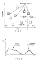
- the present invention provides improved AGC in a frequency hopping communication system in which a transmitted signal is hopping randomly in a set of independent frequencies f1 - f M , as illustrated by blocks 1 - M.
- a receiver which is designed to operate in this frequency hopping communication system knows these frequencies a priori and thus is able to follow the frequency pattern to "demodulate" the data.
- the strength of the received signal must be estimated so that the proper AGC level can be set.
- n samples are taken at the receiver.
- this transmission is a series of data pulses of a common amplitude which are transmitted as a preamble to voice communication.
- Frequency hopping voice transmission is typically initiated within a few hundred microseconds of the end of the preamble at time T.
- interference signals such as interference signals from a partial band jammer, as illustrated by the crosshatched blocks in Fig. 1, but many are not.
- a partial band jammer usually has a small duty factor, so that much energy is concentrated on these interfered frequencies.
- the signal level of the desired signal is associated with the low amplitude portion of the histogram and the interference signal is associated with the high amplitude portion of the histogram.
- the present invention makes use of the ordered statistics technique to distinguish the interference signal from the clear signal to provide a good estimate of the desired signal.
- any estimate of receiver strength (and thus the AGC selection) must have some error.
- an AGC selection is acceptable when the calculated AGC setting is within plus or minus 3 dB of the correct value. This value is selected since it defines the level at which a signal change can just be audibly detected.
- the present invention allows the optimization of the AGC performance by maximizing the probability of acceptable AGC performance. This optimization may be accomplished even in the Rayleigh fading channel in the presence of partial band jamming or impulsive type noise interference.
- Fig. 3 illustrates, in the context of a generalized HF receiver, the digital AGC sampling and control of the present invention added to a standard closed loop analog AGC circuit to provide the AGC apparatus of the present invention.
- the HF signal received through antenna 10 is converted to an intermediate frequency signal prior to the AGC circuitry.
- the HF signal may be coupled to mixer 12 where it is mixed with a signal from a first local oscillator to up convert the received signal for amplification and filtering at 14 and 16, respectively.
- the signal is then mixed with a second local oscillator signal at 18 to down convert the received signal to an intermediate frequency prior to being coupled to the AGC loop.
- the typical conventional closed loop AGC circuit includes one or more gain-controlled amplification stages 20 coupled to filter means 22, a further down-conversion stage 24 where the signal is mixed with a signal from a third local oscillator to covert the signal to audio frequency at the loop output.
- the audio frequency signal is passed through audio filter 25 to provide audio output signal.
- a portion of the audio frequency signal is coupled to an AGC generator 26 which detects the received audio level, applies the appropriate AGC attack and release time constants for either voice or data reception, and generates a direct current (DC) AGC control voltage which is applied to control the gain of the amplification stage 20.
- the AGC generator 26 provides a control voltage that increases with the level of audio signal received. It is noted that AGC may be accomplished at intermediate frequency or even at RF frequency rather than at the audio frequency level, the audio frequency level being used in this description of the preferred embodiment for purposes of illustration only.
- Typical time constants for this type of AGC circuit are: Voice mode: Attack - 30 milliseconds maximum Release - 0.75 to 1.5 seconds Data mode: Attack - 30 milliseconds maximum Release - 60 to 130 milliseconds.
- the conventional AGC loop is modified by the addition of an analog switch 28, an analog-to-digital (A/D) converter 30, a digital-to-analog (D/A) converter 32, and a digital controller 34 as follows.
- the output of the AGC generator 26 is coupled to the analog switch 28 which is connected to selectively open or close the standard AGC control loop.
- the switch 28 When the switch 28 is in a first position (as shown in Fig. 3.), the standard AGC control loop is closed and the output of the AGC generator is connected to the gain-controlled amplification stages 20.
- the switch 28 is in the second position, the output of the AGC generator is disconnected from the gain-controlled amplification stage 20 and the output of the digital-to-analog (D/A) converter 32 is coupled to the gain-controlled amplifier stage.
- the A/D converter 30 is connected to the output of the AGC generator 26 prior to the analog switch 28 in order to sample, or read, the AGC control voltage from the standard AGC control loop.
- the A/D converter 30 couples the samples of the AGC control voltage to the digital controller 34.
- the digital controller 34 is coupled (indicated by dashed line 36) to control the analog switch 28 to select the position of the switch (i.e. to select the source of the AGC control voltage).
- the Digital controller 34 is also coupled (indicated by dashed line 38) to the A/D converter 30 to control the sample time for the A/D converter and to receive the samples of the AGC generator output and to the AGC generator 26 (indicated by time.
- the digital controller 34 computes the optimum AGC control voltage based on the samples of the AGC generator output, and outputs this voltage to the D/A converter 32.
- the automatic gain control of the present invention works as follows: During the reception of known transmitted signals of duration T, the digital controller 34 closes the standard AGC loop, allowing it to track the level of the incoming signal exactly as it would in a non-frequency-hopped receiver. Periodically the digital controller 34 then samples (reads) the independent AGC voltage in the A/D converter 30 in such a way that a strong signal on one frequency hop would capture no more than one sample.
- Figs. 4 The sampling process is illustrated in Figs. 4.
- One of the primary advantages of this sampling technique is achieved when known signals in a contiguous series of frequency hops are received. Using a series of signals permits the A/D sampling process to occur a a rate slower than the hop rate.
- Fig. 4 shows an example for a hop rate of 50 hops per second (a 20 ms hop dwell time), and an AGC generator release time of 60 ms.
- the capture of an AGC sample by a interference signal is limited to interference which occurred in the preceding three hop dwells.
- the digital controller 34 calculates an optimum AGC value in accordance with the statistical method described hereinafter. The result of this calculation is then output to the D/A converter 32, the analog switch 28 is switched to discon converter 32, the analog switch 28 is switched to disconnect the AGC generator output from and to connect the output of the D/A converter to the gain controlled amplifier stage 20, thus fixing the AGC voltage at the calculated value.
- the digital controller 34 After the acquisition of the n independent samples the digital controller 34 performs an AGC selection using ordered statistics as follows.
- the n independent and identically distributed samples X1, X2, X3, ...,X N can be sorted according to amplitude as follows X[1] ⁇ X[2] ⁇ X[3] ⁇ ... X[12] ⁇ X[13] ⁇ X[14] ⁇ ... ⁇ X[N]
- the kth ordered sample, X[k] is selected.
- the selected sample is then coupled to the D/A converter 32 and the analog switch 28 is switched to connect the output of the D/A converter as the AGC control voltage.
- the analog switch 28 is switched to connect the output of the D/A converter as the AGC control voltage.
- optimum sample order k opt .
- f(x) and F(X) be the probability density function and the cumulative distribution function of the AGC samples X i , respectively.
- the probability of acceptable AGC based on the kth order sample is computed via the following equation. where n is the total number of samples collected, k is the selected order sample for the AGC setting, and the limits of the integration signify the plus and minus 3 dB levels.
- the present invention can provide a real-time adaptive AGC control when the digital controller 34 contains a microprocessor that has the processing capability necessary to solve Equation (1) for k equals 1, 2 ...,n.
- the solution of Equation (1) determines which of the ordered samples provides the highest probability of acceptable AGC.
- the value of the sample providing the highest probability of acceptable AGC is then selected for use as the AGC control voltage.
- the AGC selection can be periodically updated or even updated for each set of samples (i.e., updated each transmission of the known signals of duration T) depending on the capability of the microprocessor.
- the digital controller 34 sorts the samples X i and selects the proper sample based on the stored k opt. . The selected sample is then coupled to the D/A converter 32 for transmission amplifier 20 as the AGC control voltage.
- the probability of acceptable AGC, P(k), can be computed and the optimum selection of k opt can be found.
- the selection of optimum sample ordered is shown by line 42 in Fig. 5 as a function of the number of samples. It is observed tht the optimum selection for this case is about 2/3 of the total number of samples.
- the probability of maximum acceptable AGC is also noted. It is seen that as the number of AGC samples n increases, the probability of acceptable AGC increases. Hence having a required level of probability of acceptable AGC, the minimum required number of AGC samples and the optimum sampling order are determined.
- the channel can often be assumed as a Rayleigh fading or Rician fading channel. If the I/S ratio and the interference bandwidth factor ⁇ of the interferer can be accurately predicted, factor ⁇ of the interferer can be accurately predicted, the probability of acceptable AGC, P(k), in equation (1) can be plotted as a function of k.
- the density functions, p NI (s), and p I (s), are computed via the following formulas, Equation (5)
- I o (x) is the first order Bessel function
- N is the total number of frequencies.
- o Compute the probability of acceptable AGC, P(k), o Select k such that P(k) is maximum.
- the ordered sample X[k] is the optimum selection for the AGC setting.
- the interference bandwidth factor ⁇ may not be accurately predicted, and a receiver can be operated anywhere within ⁇ min ⁇ ⁇ ⁇ ⁇ max .
- the probability of acceptable AGC P(k) is computed and is plotted in Fig. 7 for different values of ⁇ .
- the results show that, with a good selection of ordered sample, the performance is superior compared to the slow release time AGC circuit.
Landscapes
- Engineering & Computer Science (AREA)
- Computer Networks & Wireless Communication (AREA)
- Signal Processing (AREA)
- Control Of Amplification And Gain Control (AREA)
Applications Claiming Priority (2)
| Application Number | Priority Date | Filing Date | Title |
|---|---|---|---|
| US26195488A | 1988-10-24 | 1988-10-24 | |
| US261954 | 1988-10-24 |
Publications (3)
| Publication Number | Publication Date |
|---|---|
| EP0366025A2 true EP0366025A2 (de) | 1990-05-02 |
| EP0366025A3 EP0366025A3 (de) | 1991-02-27 |
| EP0366025B1 EP0366025B1 (de) | 1994-07-20 |
Family
ID=22995592
Family Applications (1)
| Application Number | Title | Priority Date | Filing Date |
|---|---|---|---|
| EP19890119554 Expired - Lifetime EP0366025B1 (de) | 1988-10-24 | 1989-10-21 | Automatische Verstärkungsregelung für Frequenzsprungempfänger |
Country Status (3)
| Country | Link |
|---|---|
| EP (1) | EP0366025B1 (de) |
| DE (1) | DE68916899T2 (de) |
| IL (1) | IL92021A (de) |
Cited By (10)
| Publication number | Priority date | Publication date | Assignee | Title |
|---|---|---|---|---|
| EP0496507A2 (de) * | 1991-01-15 | 1992-07-29 | Nokia Mobile Phones Ltd. | Verstärkungsregelung für Funktelefoniersystem TDMA |
| EP0630106A1 (de) * | 1993-06-04 | 1994-12-21 | Matsushita Electric Industrial Co., Ltd. | Vorrichtung zur automatischer Verstärkungsregelung |
| GB2281157A (en) * | 1993-08-16 | 1995-02-22 | Aeg Mobile Communication | Gain control using sampling suitable for TDMA systems |
| WO1995030288A1 (en) * | 1994-04-28 | 1995-11-09 | Linkplus Corporation | Frequency synchronization for frequency hopping communication using calibration tone sent at hop |
| EP0926837A1 (de) * | 1996-06-25 | 1999-06-30 | Nec Corporation | Automatische Verstärkungsregelung für Frequenzsprungkommunikationsempfänger |
| WO2008117130A1 (en) * | 2007-03-27 | 2008-10-02 | Freescale Semiconductor, Inc. | Method and apparatus for varying a dynamic range |
| EP1998441A2 (de) * | 2007-05-25 | 2008-12-03 | Thales | Automatische Kontrolle der Verstärkung infolge der Wahrscheinlichkeitsdichte der empfangenen Leistung |
| EP2127098A1 (de) * | 2006-12-25 | 2009-12-02 | Thomson Licensing | Verfahren und einrichtung zur automatischen verstärkungsregelung |
| CN102386869A (zh) * | 2010-08-27 | 2012-03-21 | 杭州中科微电子有限公司 | 一种模拟/数字可配置可变增益放大器 |
| US11476818B2 (en) | 2018-06-27 | 2022-10-18 | Nordic Semiconductor Asa | Automatic gain control |
Families Citing this family (2)
| Publication number | Priority date | Publication date | Assignee | Title |
|---|---|---|---|---|
| DE19829500A1 (de) * | 1998-07-02 | 2000-01-13 | Thomson Brandt Gmbh | Verfahren zur Verbesserung des Nutzsignals in einer Funkempfangseinheit |
| DE102005037617A1 (de) * | 2005-08-09 | 2007-02-15 | Rohde & Schwarz Gmbh & Co. Kg | Vorrichtung und Verfahren zum Begrenzen von Störamplituden |
Citations (1)
| Publication number | Priority date | Publication date | Assignee | Title |
|---|---|---|---|---|
| GB2149245A (en) * | 1983-10-29 | 1985-06-05 | Plessey Co Plc | A.G.C. system |
-
1989
- 1989-10-17 IL IL9202189A patent/IL92021A/en not_active IP Right Cessation
- 1989-10-21 EP EP19890119554 patent/EP0366025B1/de not_active Expired - Lifetime
- 1989-10-21 DE DE1989616899 patent/DE68916899T2/de not_active Expired - Fee Related
Patent Citations (1)
| Publication number | Priority date | Publication date | Assignee | Title |
|---|---|---|---|---|
| GB2149245A (en) * | 1983-10-29 | 1985-06-05 | Plessey Co Plc | A.G.C. system |
Non-Patent Citations (1)
| Title |
|---|
| IEEE TRANSACTIONS ON INFORMATION THEORY, vol. IT-17, no. 5, September 1971, pages 625-627; C.-P. WANG et al.: "Adaptive gain control" * |
Cited By (22)
| Publication number | Priority date | Publication date | Assignee | Title |
|---|---|---|---|---|
| EP0496507A2 (de) * | 1991-01-15 | 1992-07-29 | Nokia Mobile Phones Ltd. | Verstärkungsregelung für Funktelefoniersystem TDMA |
| EP0496507A3 (en) * | 1991-01-15 | 1993-06-30 | Nokia Mobile Phones Ltd. | Gain control in a tdma radio-telephone system |
| US5331638A (en) * | 1991-01-15 | 1994-07-19 | Nokia Mobile Phones Ltd. | Gain control in a TDMA radio-telephone system |
| EP0630106A1 (de) * | 1993-06-04 | 1994-12-21 | Matsushita Electric Industrial Co., Ltd. | Vorrichtung zur automatischer Verstärkungsregelung |
| US5450035A (en) * | 1993-06-04 | 1995-09-12 | Matsushita Electric Industrial Co., Ltd. | Automatic gain control apparatus |
| CN1073762C (zh) * | 1993-06-04 | 2001-10-24 | 松下电器产业株式会社 | 自动增益控制装置 |
| GB2281157A (en) * | 1993-08-16 | 1995-02-22 | Aeg Mobile Communication | Gain control using sampling suitable for TDMA systems |
| FR2709215A1 (fr) * | 1993-08-16 | 1995-02-24 | Aeg Mobile Communication | Proccédé de réglage automatique de l'amplification dans un récepteur. |
| GB2281157B (en) * | 1993-08-16 | 1998-10-14 | Aeg Mobile Communication | Method for automatically controlling the amplification in a receiver |
| WO1995030288A1 (en) * | 1994-04-28 | 1995-11-09 | Linkplus Corporation | Frequency synchronization for frequency hopping communication using calibration tone sent at hop |
| US5995816A (en) * | 1996-06-25 | 1999-11-30 | Nec Corporation | Frequency hopping communications receivers |
| EP0926837A1 (de) * | 1996-06-25 | 1999-06-30 | Nec Corporation | Automatische Verstärkungsregelung für Frequenzsprungkommunikationsempfänger |
| EP2127098A1 (de) * | 2006-12-25 | 2009-12-02 | Thomson Licensing | Verfahren und einrichtung zur automatischen verstärkungsregelung |
| EP2127098A4 (de) * | 2006-12-25 | 2010-05-19 | Thomson Licensing | Verfahren und einrichtung zur automatischen verstärkungsregelung |
| CN101601190B (zh) * | 2006-12-25 | 2013-01-16 | 汤姆逊许可公司 | 自动增益控制方法和设备 |
| WO2008117130A1 (en) * | 2007-03-27 | 2008-10-02 | Freescale Semiconductor, Inc. | Method and apparatus for varying a dynamic range |
| US8126101B2 (en) | 2007-03-27 | 2012-02-28 | Freescale Semiconductor, Inc. | Method and apparatus for varying a dynamic range |
| EP1998441A2 (de) * | 2007-05-25 | 2008-12-03 | Thales | Automatische Kontrolle der Verstärkung infolge der Wahrscheinlichkeitsdichte der empfangenen Leistung |
| EP1998441A3 (de) * | 2007-05-25 | 2009-03-04 | Thales | Automatische Kontrolle der Verstärkung infolge der Wahrscheinlichkeitsdichte der empfangenen Leistung |
| CN102386869A (zh) * | 2010-08-27 | 2012-03-21 | 杭州中科微电子有限公司 | 一种模拟/数字可配置可变增益放大器 |
| US11476818B2 (en) | 2018-06-27 | 2022-10-18 | Nordic Semiconductor Asa | Automatic gain control |
| US11804812B2 (en) | 2018-06-27 | 2023-10-31 | Nordic Semiconductor Asa | Automatic gain control |
Also Published As
| Publication number | Publication date |
|---|---|
| IL92021A (en) | 1994-06-24 |
| DE68916899T2 (de) | 1994-11-10 |
| EP0366025B1 (de) | 1994-07-20 |
| DE68916899D1 (de) | 1994-08-25 |
| EP0366025A3 (de) | 1991-02-27 |
Similar Documents
| Publication | Publication Date | Title |
|---|---|---|
| US5267272A (en) | Receiver automatic gain control (AGC) | |
| US5029182A (en) | Automatic gain control (AGC) for frequency hopping receiver | |
| KR100329673B1 (ko) | 직각수신기에서dc오프세트소거및자동이득제어를위한방법및장치 | |
| US4742563A (en) | System and method for diversity reception of signals | |
| KR100273492B1 (ko) | 확산스펙트럼 신호용 무선수신기 | |
| US7522556B2 (en) | Signal recognition in an on-frequency repeater | |
| US5907798A (en) | Wireless telephone intermodulation performance enhancement techniques | |
| US5809400A (en) | Intermodulation performance enhancement by dynamically controlling RF amplifier current | |
| EP0542520B1 (de) | Regelbarer Filter | |
| EP0913934B1 (de) | Empfängervorrichtung | |
| US6067333A (en) | Adaptive serial and parallel mixed interference cancellation method | |
| US5909645A (en) | Receiver with dynamic attenuation control for adaptive intermodulation performance enhancement | |
| US5386495A (en) | Method and apparatus for determining the signal quality of a digital signal | |
| EP0366025A2 (de) | Automatische Verstärkungsregelung für Frequenzsprungempfänger | |
| EP0361299A2 (de) | Digitales Funkübertragungssystem für ein aus Zellen aufgebautes Netz unter Verwendung der Bandspreiztechnik | |
| EP0556360B1 (de) | Verfahren zur selbsttätigen sendeleistungssteuerung in einem einer cdma-umgebung angepassten senderempfänger unter verwendung einer direktsequenzspreizung | |
| EP1061643B1 (de) | Empfänger und Verfahren zur Regelung der Verstärkung desselben | |
| EP1324504A2 (de) | Radioempfänger und Radioempfangsverfahren | |
| KR20030065533A (ko) | 간섭 분류 방법 및 장치 | |
| US6192226B1 (en) | Carrier squelch processing system and apparatus | |
| AU635134B2 (en) | Digital automatic gain control | |
| EP0926837B1 (de) | Automatische Verstärkungsregelung für Frequenzsprungkommunikationsempfänger | |
| KR101210608B1 (ko) | 임펄스 신호기반 초광대역 무선통신 시스템의 효율적 수신구조를 이용한 자동 이득 제어 장치 및 방법 | |
| EP1221777B1 (de) | Verfahren und Vorrichtung zur Interferenz-Klassifikation | |
| CN115276694A (zh) | 一种跳频接收机及其增益自动控制方法 |
Legal Events
| Date | Code | Title | Description |
|---|---|---|---|
| PUAI | Public reference made under article 153(3) epc to a published international application that has entered the european phase |
Free format text: ORIGINAL CODE: 0009012 |
|
| 17P | Request for examination filed |
Effective date: 19891113 |
|
| AK | Designated contracting states |
Kind code of ref document: A2 Designated state(s): DE FR GB |
|
| PUAL | Search report despatched |
Free format text: ORIGINAL CODE: 0009013 |
|
| AK | Designated contracting states |
Kind code of ref document: A3 Designated state(s): DE FR GB |
|
| RHK1 | Main classification (correction) |
Ipc: H04B 1/66 |
|
| 17Q | First examination report despatched |
Effective date: 19930322 |
|
| GRAA | (expected) grant |
Free format text: ORIGINAL CODE: 0009210 |
|
| AK | Designated contracting states |
Kind code of ref document: B1 Designated state(s): DE FR GB |
|
| REF | Corresponds to: |
Ref document number: 68916899 Country of ref document: DE Date of ref document: 19940825 |
|
| ET | Fr: translation filed | ||
| PLBE | No opposition filed within time limit |
Free format text: ORIGINAL CODE: 0009261 |
|
| STAA | Information on the status of an ep patent application or granted ep patent |
Free format text: STATUS: NO OPPOSITION FILED WITHIN TIME LIMIT |
|
| 26N | No opposition filed | ||
| REG | Reference to a national code |
Ref country code: GB Ref legal event code: 732E |
|
| REG | Reference to a national code |
Ref country code: GB Ref legal event code: IF02 |
|
| PGFP | Annual fee paid to national office [announced via postgrant information from national office to epo] |
Ref country code: FR Payment date: 20031125 Year of fee payment: 15 |
|
| PGFP | Annual fee paid to national office [announced via postgrant information from national office to epo] |
Ref country code: DE Payment date: 20031128 Year of fee payment: 15 |
|
| PGFP | Annual fee paid to national office [announced via postgrant information from national office to epo] |
Ref country code: GB Payment date: 20040112 Year of fee payment: 15 |
|
| PG25 | Lapsed in a contracting state [announced via postgrant information from national office to epo] |
Ref country code: GB Free format text: LAPSE BECAUSE OF NON-PAYMENT OF DUE FEES Effective date: 20041021 |
|
| PG25 | Lapsed in a contracting state [announced via postgrant information from national office to epo] |
Ref country code: DE Free format text: LAPSE BECAUSE OF NON-PAYMENT OF DUE FEES Effective date: 20050503 |
|
| GBPC | Gb: european patent ceased through non-payment of renewal fee |
Effective date: 20041021 |
|
| PG25 | Lapsed in a contracting state [announced via postgrant information from national office to epo] |
Ref country code: FR Free format text: LAPSE BECAUSE OF NON-PAYMENT OF DUE FEES Effective date: 20050630 |
|
| REG | Reference to a national code |
Ref country code: FR Ref legal event code: ST |
|
| REG | Reference to a national code |
Ref country code: GB Ref legal event code: 732E Free format text: REGISTERED BETWEEN 20090910 AND 20090916 |
|
| REG | Reference to a national code |
Ref country code: GB Ref legal event code: 732E Free format text: REGISTERED BETWEEN 20090917 AND 20090923 |