EP0364551B1 - Thermal expansion mismatch forgivable printed wiring board for ceramic leadless chip carrier - Google Patents
Thermal expansion mismatch forgivable printed wiring board for ceramic leadless chip carrier Download PDFInfo
- Publication number
- EP0364551B1 EP0364551B1 EP89904061A EP89904061A EP0364551B1 EP 0364551 B1 EP0364551 B1 EP 0364551B1 EP 89904061 A EP89904061 A EP 89904061A EP 89904061 A EP89904061 A EP 89904061A EP 0364551 B1 EP0364551 B1 EP 0364551B1
- Authority
- EP
- European Patent Office
- Prior art keywords
- layer
- printed wiring
- wiring board
- chip carrier
- expansion
- Prior art date
- Legal status (The legal status is an assumption and is not a legal conclusion. Google has not performed a legal analysis and makes no representation as to the accuracy of the status listed.)
- Expired - Lifetime
Links
Images
Classifications
-
- H—ELECTRICITY
- H05—ELECTRIC TECHNIQUES NOT OTHERWISE PROVIDED FOR
- H05K—PRINTED CIRCUITS; CASINGS OR CONSTRUCTIONAL DETAILS OF ELECTRIC APPARATUS; MANUFACTURE OF ASSEMBLAGES OF ELECTRICAL COMPONENTS
- H05K1/00—Printed circuits
- H05K1/02—Details
- H05K1/0271—Arrangements for reducing stress or warp in rigid printed circuit boards, e.g. caused by loads, vibrations or differences in thermal expansion
-
- B—PERFORMING OPERATIONS; TRANSPORTING
- B32—LAYERED PRODUCTS
- B32B—LAYERED PRODUCTS, i.e. PRODUCTS BUILT-UP OF STRATA OF FLAT OR NON-FLAT, e.g. CELLULAR OR HONEYCOMB, FORM
- B32B7/00—Layered products characterised by the relation between layers; Layered products characterised by the relative orientation of features between layers, or by the relative values of a measurable parameter between layers, i.e. products comprising layers having different physical, chemical or physicochemical properties; Layered products characterised by the interconnection of layers
- B32B7/02—Physical, chemical or physicochemical properties
- B32B7/027—Thermal properties
-
- H—ELECTRICITY
- H05—ELECTRIC TECHNIQUES NOT OTHERWISE PROVIDED FOR
- H05K—PRINTED CIRCUITS; CASINGS OR CONSTRUCTIONAL DETAILS OF ELECTRIC APPARATUS; MANUFACTURE OF ASSEMBLAGES OF ELECTRICAL COMPONENTS
- H05K3/00—Apparatus or processes for manufacturing printed circuits
- H05K3/46—Manufacturing multilayer circuits
- H05K3/4611—Manufacturing multilayer circuits by laminating two or more circuit boards
- H05K3/4623—Manufacturing multilayer circuits by laminating two or more circuit boards the circuit boards having internal via connections between two or more circuit layers before lamination, e.g. double-sided circuit boards
-
- H—ELECTRICITY
- H05—ELECTRIC TECHNIQUES NOT OTHERWISE PROVIDED FOR
- H05K—PRINTED CIRCUITS; CASINGS OR CONSTRUCTIONAL DETAILS OF ELECTRIC APPARATUS; MANUFACTURE OF ASSEMBLAGES OF ELECTRICAL COMPONENTS
- H05K1/00—Printed circuits
- H05K1/02—Details
- H05K1/11—Printed elements for providing electric connections to or between printed circuits
- H05K1/118—Printed elements for providing electric connections to or between printed circuits specially for flexible printed circuits, e.g. using folded portions
-
- H—ELECTRICITY
- H05—ELECTRIC TECHNIQUES NOT OTHERWISE PROVIDED FOR
- H05K—PRINTED CIRCUITS; CASINGS OR CONSTRUCTIONAL DETAILS OF ELECTRIC APPARATUS; MANUFACTURE OF ASSEMBLAGES OF ELECTRICAL COMPONENTS
- H05K2201/00—Indexing scheme relating to printed circuits covered by H05K1/00
- H05K2201/01—Dielectrics
- H05K2201/0104—Properties and characteristics in general
- H05K2201/0133—Elastomeric or compliant polymer
-
- H—ELECTRICITY
- H05—ELECTRIC TECHNIQUES NOT OTHERWISE PROVIDED FOR
- H05K—PRINTED CIRCUITS; CASINGS OR CONSTRUCTIONAL DETAILS OF ELECTRIC APPARATUS; MANUFACTURE OF ASSEMBLAGES OF ELECTRICAL COMPONENTS
- H05K2201/00—Indexing scheme relating to printed circuits covered by H05K1/00
- H05K2201/01—Dielectrics
- H05K2201/0137—Materials
- H05K2201/015—Fluoropolymer, e.g. polytetrafluoroethylene [PTFE]
-
- H—ELECTRICITY
- H05—ELECTRIC TECHNIQUES NOT OTHERWISE PROVIDED FOR
- H05K—PRINTED CIRCUITS; CASINGS OR CONSTRUCTIONAL DETAILS OF ELECTRIC APPARATUS; MANUFACTURE OF ASSEMBLAGES OF ELECTRICAL COMPONENTS
- H05K2201/00—Indexing scheme relating to printed circuits covered by H05K1/00
- H05K2201/01—Dielectrics
- H05K2201/0137—Materials
- H05K2201/0154—Polyimide
-
- H—ELECTRICITY
- H05—ELECTRIC TECHNIQUES NOT OTHERWISE PROVIDED FOR
- H05K—PRINTED CIRCUITS; CASINGS OR CONSTRUCTIONAL DETAILS OF ELECTRIC APPARATUS; MANUFACTURE OF ASSEMBLAGES OF ELECTRICAL COMPONENTS
- H05K2201/00—Indexing scheme relating to printed circuits covered by H05K1/00
- H05K2201/06—Thermal details
- H05K2201/068—Thermal details wherein the coefficient of thermal expansion is important
-
- H—ELECTRICITY
- H05—ELECTRIC TECHNIQUES NOT OTHERWISE PROVIDED FOR
- H05K—PRINTED CIRCUITS; CASINGS OR CONSTRUCTIONAL DETAILS OF ELECTRIC APPARATUS; MANUFACTURE OF ASSEMBLAGES OF ELECTRICAL COMPONENTS
- H05K2201/00—Indexing scheme relating to printed circuits covered by H05K1/00
- H05K2201/09—Shape and layout
- H05K2201/09009—Substrate related
- H05K2201/09109—Locally detached layers, e.g. in multilayer
-
- H—ELECTRICITY
- H05—ELECTRIC TECHNIQUES NOT OTHERWISE PROVIDED FOR
- H05K—PRINTED CIRCUITS; CASINGS OR CONSTRUCTIONAL DETAILS OF ELECTRIC APPARATUS; MANUFACTURE OF ASSEMBLAGES OF ELECTRICAL COMPONENTS
- H05K2201/00—Indexing scheme relating to printed circuits covered by H05K1/00
- H05K2201/09—Shape and layout
- H05K2201/09209—Shape and layout details of conductors
- H05K2201/095—Conductive through-holes or vias
- H05K2201/09536—Buried plated through-holes, i.e. plated through-holes formed in a core before lamination
-
- H—ELECTRICITY
- H05—ELECTRIC TECHNIQUES NOT OTHERWISE PROVIDED FOR
- H05K—PRINTED CIRCUITS; CASINGS OR CONSTRUCTIONAL DETAILS OF ELECTRIC APPARATUS; MANUFACTURE OF ASSEMBLAGES OF ELECTRICAL COMPONENTS
- H05K2201/00—Indexing scheme relating to printed circuits covered by H05K1/00
- H05K2201/10—Details of components or other objects attached to or integrated in a printed circuit board
- H05K2201/10613—Details of electrical connections of non-printed components, e.g. special leads
- H05K2201/10621—Components characterised by their electrical contacts
- H05K2201/10727—Leadless chip carrier [LCC], e.g. chip-modules for cards
-
- H—ELECTRICITY
- H05—ELECTRIC TECHNIQUES NOT OTHERWISE PROVIDED FOR
- H05K—PRINTED CIRCUITS; CASINGS OR CONSTRUCTIONAL DETAILS OF ELECTRIC APPARATUS; MANUFACTURE OF ASSEMBLAGES OF ELECTRICAL COMPONENTS
- H05K3/00—Apparatus or processes for manufacturing printed circuits
- H05K3/0058—Laminating printed circuit boards onto other substrates, e.g. metallic substrates
- H05K3/0061—Laminating printed circuit boards onto other substrates, e.g. metallic substrates onto a metallic substrate, e.g. a heat sink
-
- H—ELECTRICITY
- H05—ELECTRIC TECHNIQUES NOT OTHERWISE PROVIDED FOR
- H05K—PRINTED CIRCUITS; CASINGS OR CONSTRUCTIONAL DETAILS OF ELECTRIC APPARATUS; MANUFACTURE OF ASSEMBLAGES OF ELECTRICAL COMPONENTS
- H05K3/00—Apparatus or processes for manufacturing printed circuits
- H05K3/30—Assembling printed circuits with electric components, e.g. with resistors
- H05K3/32—Assembling printed circuits with electric components, e.g. with resistors electrically connecting electric components or wires to printed circuits
- H05K3/34—Assembling printed circuits with electric components, e.g. with resistors electrically connecting electric components or wires to printed circuits by soldering
- H05K3/341—Surface mounted components
- H05K3/3431—Leadless components
- H05K3/3442—Leadless components having edge contacts, e.g. leadless chip capacitors, chip carriers
Definitions
- the present invention relates to a printed wiring board for mounting a ceramic leadless chip carrier and to a method for forming a printed wiring board and relates generally to the surface mounting of ceramic leadless chip carriers to printed wiring boards. More particularly, the present invention relates to methods and apparatus for increasing the reliability of the solder joint integrity between the printed wiring board and the chip carrier.
- a printed wiring board comprising a substrate, a patterned layer of adhesive, a patterned metal layer, an electrical component, and connections.
- the adhesive is patterned to have an opening whose length exceeds that of the component to be soldered. The opening is sufficiently long to permit adaptation to the mechanical and thermal characteristics of the substrate and component.
- the ceramic leadless chip carrier is mounted to the printed wiring board surface by way of solder fillets or joints. It is important that the integrity and reliability of the solder joint be maintained for long periods of time and be able to withstand numerous temperature and power cycles. In addition, the solder joint must be able to withstand shock and vibration which may occur in many electronic systems such as those used in avionics.
- the present invention in accordance with claims 1 and 12 provides an improved method and apparatus for mounting ceramic leadless chip carriers to printed wiring boards wherein the chances of solder joint cracking are reduced to thereby increase the reliability and integrity of the system.
- the present invention is based upon fabricating the printed wiring circuit board so that the top layer of the board expands and contracts with the chip carrier regardless of the expansion or contraction rates of the main body of the wiring board.
- the printed wiring board in accordance with claim 1 includes an expansion layer having a bottom surface and top surface wherein the top surface of the expansion layer forms the top surface of the printed wiring board.
- the expansion layer is supported by a rigid support layer which also has a top and a bottom.
- the bottom of the expansion layer is bonded to the top of the rigid support layer except in the area located directly below the footprint of the chip carrier and solder joints. This lack of bonding between the expansion layer and rigid support layer provides a forgivable expansion area located underneath the chip carrier footprint wherein the expansion layer can expand and contract the same amount as the chip carrier irrespective of the expansion and contraction rates of the rigid support layers.
- the expansion layer is relatively thin and flexible, and the leadless chip carrier solder joint stress caused by thermal expansion mismatch between the leadless chip carrier and the expansion layer is extremely low so that the chances for solder joint cracking are reduced.
- a polytetrafluoroethylene (PTFE) dispersion or emulsion may be applied onto the bottom of the expansion layer at those locations where bonding is not desired.
- the PTFE dispersion is then dried and cured to form non-bonding areas. Subsequent bonding of the expansion layer to the rigid support layer provides bonding everywhere except at the non-bonding locations provided by the PTFE layer.
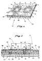
- a preferred printed wiring board in accordance with the present invention is shown generally at 10 in FIGS. 1, 2 and 3.
- the printed wiring board 10 is shown in FIG. 1 prior to mounting of the ceramic leadless chip carriers.
- the board 10 includes a plurality of chip carrier mounting pads 12. Circuit lines connecting the various circuitry are shown at 14. Via holes are shown at 16. The circuit lines and via holes are provided for illustration purposes only since these are conventional features of any printed wiring board and do not form a part of the invention.
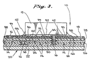
- a detailed sectional view of a portion of the printed wiring board 10 is shown in FIG. 2 after the ceramic leadless chip carrier 13 is mounted thereon.
- the preferred printed wiring board includes an expansion layer 18 which is bonded to a rigid support layer shown generally at 20.
- the support layer 20 is a multi-layer laminated board, which as best shown in FIG. 2, includes a metal plate 22, thermally conductive adhesive layer 24, and polyimide impregnated glass fiber layers 26 and 28 (referred to herein as polyimide fiberglass) which are bonded together by adhesive layer 30.
- the metal plate 22 is optional. As is well known, metal plates are included as part of a printed wiring board where it is desirable to thermally conduct heat away from the printed wiring board and where added strength is desired. If a metal plate 22 is used, it is desirable to use a thermally conductive adhesive 24 in order to ensure that heat from the printed wiring board is conducted to the metal plate 22.
- the polyimide fiberglass layers 26 and 28 do not necessarily have to be made of polyimide fiberglass.
- Other suitable printed wiring board materials such as epoxy fiberglass, polyimide quartz fibers, alumina (ceramic) fiber substrates, polyimide aramid fibers and any other suitable composite materials typically used in printed wiring boards can also be used as the printed wiring board layers.
- the adhesive layer 30 which is used to bond the layers 26 and 28 together may also be any of the conventionally known adhesives commonly used in preparing laminated printed wiring boards. Examples of suitable adhesives include epoxy prepreg, polyimide prepreg, etc.
- a metal layer 22 When a metal layer 22 is used, it will preferably have a thickness of between about 0.076 cm to 0.76 cm (0.030 inch to 0.300 inch), most preferably between about 0.13 cm to 0.76 cm (0.050 inch to 0.300 inch).
- the polyimide fiberglass layers 26 and 28 preferably have thicknesses of between about 0.010 cm to 0.64 cm (0.004 inch to 0.25 inch), most preferably to 0.23 cm (0.090 inch).
- the thickness of the two adhesive layers 24 and 30 are preferably between about 0.010 cm to 0.030 cm (0.004 inch to 0.012 inch).
- the particular metal used for the metal layer can be any of those conventionally used in printed wiring boards including aluminum, copper and copper alloys and any other suitable thermally conductive metal.
- an expansion layer 18 is provided.
- the expansion layer 18 includes a top 32 and bottom 34.
- the bottom 34 of expansion layer 18 is bonded to the top 36 of the support layer 20 by way of adhesive layer 38.
- the adhesive layer 38 is not bonded to the expansion layer 18 underneath the chip carrier 13. This leaves an unbonded area 40 where the expansion layer 18 is not attached to the support layer 20.
- a layer of polytetrafluoroethylene (PTFE) 39 is provided which prevents adhesion of the support layer 20 to the expansion layer 18.
- the chip carrier 13 is mounted onto the top 32 of expansion layer 18 by way of solder fillets or joints 42.
- the area under the chip carrier 13 and solder joints 42 is defined as the footprint of the chip carrier.
- the adhesive layer 38 provides no bonding at locations beneath the chip carrier footprint. The area of non-bonding will extend slightly outward from the footprint as best shown at 44 and 46 in FIG. 2. This provides a non-bonded portion of the expansion layer 18 which does not lie directly beneath the chip carrier footprint. It is essential that this extra non-bonded portion be provided.
- the expansion layer 18 is made from a material having low modulus of elasticity, such as a polyimide film.
- a polyimide film is marketed by E. I. DuPont under the trade name KAPTON.
- Other flexible films are possible so long as they have properties similar to polyimide including high temperature stability and good bonding characteristics. These films should not contain fillers, such as glass particles or beads which might adversely affect the flexibility of the film.
- the thickness of the expansion layer should be such that it has some degree of flexibility while still being structurally strong. Layer thicknesses of between 0.001 cm to 0.013 cm (0.0005 inch to 0.005 inch) are suitable. Suitable adhesives for attaching the expansion layer 18 to the support layer 20 include no-flow type adhesives such as polyimide prepreg, epoxy prepreg, etc. The thickness of the adhesive layer should be less than about 0.25 cm (0.10 inch).
- any suitable fabrication technique can be utilized in order to insure that the expansion layer 18 is not bonded to the top 36 of support layer 20 at locations under the chip carrier footprint.
- the unbonded footprint area 40 can be achieved by die cutting the prepreg adhesive layer or by applying various mold release agents on the bottom 34 of expansion layer 18 to prevent the adhesive 38 from adhering to the area below the chip carrier.
- layers or sheets of conventional release materials may be inserted between the expansion layer bottom 34 and the top 36 of support layer 20.
- the unbonded footprint area 40 is provided by applying a thin layer of an emulsion of polytetrafluoroethylene (PTFE) to the bottom 34 of expansion layer 18.
- PTFE polytetrafluoroethylene
- the PTFE emulsion is dried and then fused at high temperature to provide a well defined PTFE layer 39 which prevents the adhesive layer 38 from bonding to the expansion layer bottom 34.
- the PTFE emulsion is preferably an aqueous suspension of very fine PTFE particles.
- the particle sizes are preferably between about 0.1 to 0.25 ⁇ m (microns).
- the emulsion is preferably applied by silkscreening onto the expansion layer bottom 34.
- the concentration of PTFE in the aqueous emulsion should be between 55-75 percent by weight depending upon the pore size of the silkscreen used. A PTFE concentration of about 65 weight percent was found to work well when silkscreens having a pore size of 325 mesh are used.
- the silkscreening process is carried out according to conventional silkscreening techniques which are well known.
- the PTFE particles include a coating of wetting agent to help maintain an aqueous emulsion of the particles.
- PTFE particles having a wetting agent coating are available from DuPont Chemical Corp. as TEFLON 120-FEP Dispersion. The identity of the wetting agent used on the TEFLON 120 particles is not known; however, it is believed that any known wetting agent can be used provided that it produces the desired emulsion characteristics and can be evaporated by heating or otherwise removed from the PTFE prior to or during fusion.
- a 65 weight percent aqueous emulsion of TEFLON 120-FEP Dispersion was prepared.
- the solution was selectively silkscreened onto a flexible polyimide sheet using a 325 mesh silkscreen.
- the emulsion was dried at 125°C for 30 minutes followed by baking at 260°C (500°F) to remove the coating of wetting agent.
- the remaining PTFE particles were then fused at 274°C (525°F) to form a solid well-defined layer of PTFE.
- the PTFE layer prevents the adhesive layer from bonding to the flexible polyimide sheet at the PTFE layer locations when the flexible sheet is bonded to the circuit board as previously described.
- the PTFE should be relatively pure. However, minor amounts of impurities or additives are possible provided that the non-bonding characteristics of the PTFE relative to the adhesive layer are not lost.
- the PTFE particles may also be selectively applied by spraying or other techniques that can provide the same well-defined surface application provided by silk-screening of aqueous emulsions.
- Methyl ethyl ketone (MEK) and other suitable solvents can be used for spray application provided that they do not flash off too quickly when the emulsion is sprayed.
- Acetone does not work well as a solvent or carrier for the PTFE particles for spraying or silkscreening because it flashes off too quickly.
- the final PTFE layer 39, after fusion, should be as thin as possible while still preventing bonding between the flexible expansion layer 18 and support layer 20.
- PTFE layer thicknesses on the order of 0.0002 cm to 0.0006 cm (0.0001 inch to 0.0003 inch) are preferred.
- the temperature for fusion of the particles should be around 274°C (525°F) or higher. Temperatures above 282°C 540°F are preferred because it reduces the time required for fusion of the particles into a thin layer.
- the PTFE emulsion may be applied to the support layer 28 instead of the expansion layer 18. In either case, the fused PTFE layer will prevent bonding between the expansion layer 18 and support layer 28 when the adhesive is applied. However, it is preferred to apply the PTFE emulsion to the expansion layer 18.
- LCCC leadless ceramic chip carriers
- the LCCC's included a polyimide glass printed wiring board (PWB) assembly which was 0.24 cm (0.09 inch) thick.
- PWB polyimide glass printed wiring board
- the expansion layer was flexible polyimide sheet made by Enka having a thickness of 0.002 cm (0.001 inch).
- a vibration test was performed. The purpose of this test was to find out whether any damage would occur under vibration in the following areas: the LCCC solder joint, the thin flexible expansion layer in the unbonded area, and the PWB itself. The test results showed that this PWB could take high vibration input without any damage.
- the LCCC solder joints of more rigid PWBs have a better chance for surviving the vibration test because rigid boards have a high resonance frequency.
- the solder joints of the LCCC have high stresses. If the natural frequency of the PWB is higher than the electronic system's operating vibration frequency (fans, motors, etc.), the vibration will have a minimum effect on the reliability of the PWBs.
- the PWB When the PWB is resonant, it vibrates in a waveform. This waveform tends to pull the PWB away from the LCCC causing high stress on its solder joint.
- the compliant-layer PWB of the present invention does not have very high rigidity if no heat sink is used. However, the compliant-layer PWB functions differently from regular PWBs.
- the thin, flexible, top layer tolerates placement mismatch between the LCCC and the PWB because the thin layer can stretch or compress without creating high stress on the solder joint. This provides a solution to the solder joint failure (due to vibration) of the surface mount device.
- thermal shock tests were performed. The test procedure was as follows. All of the PWBs were placed into a thermal shock machine. These boards were alternately shifted from a hot chamber to a cold chamber and vice versa. The temperature of the hot chamber was +125°C, and the cold chamber was -55°C. The duration of the PWBs stay in each chamber was 20 minutes.
- the chip resistors were bonded on the center cavity of the LCCCs. It had the same arrangement as the one used for power cycling.
- the thermocouples were mounted in the LCCC cavity on the LCCC wall, and on the PWB. The power consumption of each LCCC and the temperature of each thermocouple were measured. The thermal impedance of the PWB was calculated. The test results showed that the compliant-layer PWB had the same thermal character as the regular polyimide glass PWB.
Landscapes
- Engineering & Computer Science (AREA)
- Microelectronics & Electronic Packaging (AREA)
- Physics & Mathematics (AREA)
- Thermal Sciences (AREA)
- Manufacturing & Machinery (AREA)
- Laminated Bodies (AREA)
- Production Of Multi-Layered Print Wiring Board (AREA)
- Structures For Mounting Electric Components On Printed Circuit Boards (AREA)
- Electric Connection Of Electric Components To Printed Circuits (AREA)
Abstract
Description
- The present invention relates to a printed wiring board for mounting a ceramic leadless chip carrier and to a method for forming a printed wiring board and relates generally to the surface mounting of ceramic leadless chip carriers to printed wiring boards. More particularly, the present invention relates to methods and apparatus for increasing the reliability of the solder joint integrity between the printed wiring board and the chip carrier.
- From EP-A-0 044 247 a printed wiring board is known comprising a substrate, a patterned layer of adhesive, a patterned metal layer, an electrical component, and connections. The adhesive is patterned to have an opening whose length exceeds that of the component to be soldered. The opening is sufficiently long to permit adaptation to the mechanical and thermal characteristics of the substrate and component.
- The surface mounting of electronic devices, such as ceramic leadless chip carriers, has become popular due to the ability to save weight and volume in electronic equipment when such surface-mount technology is used. In addition, the need for increased circuit density makes surface mounting of chip carriers even more desirable.
- Typically, the ceramic leadless chip carrier is mounted to the printed wiring board surface by way of solder fillets or joints. It is important that the integrity and reliability of the solder joint be maintained for long periods of time and be able to withstand numerous temperature and power cycles. In addition, the solder joint must be able to withstand shock and vibration which may occur in many electronic systems such as those used in avionics.
- The increasing popularity of surface mounting of ceramic leadless chip carriers has brought with it concerns over the reliability and integrity of the solder joints between the chip carriers and the printed wiring board. Cracking and other disturbances to the joint integrity have been noted. Joint cracking is believed to be due mainly to differences in the thermal coefficients of expansion between the printed wiring board and the chip carriers. Various different approaches have been taken to reduce the possibility of solder joint cracking. These approaches have included making the printed wiring board out of materials having thermal coefficients of expansion which are close to the thermal coefficient of expansion for the ceramic leadless chip carriers. In addition, attempts have been made to replace the solder joint with a joint which is less likely to crack, such as electrically conductive epoxy compounds. Although the various approaches used to date have experienced different degrees of success, there still is a continuing need to provide a method for surface mounting ceramic leadless chip carriers to printed wiring boards wherein the possibility of solder joint cracking is eliminated.
- The present invention in accordance with
claims 1 and 12 provides an improved method and apparatus for mounting ceramic leadless chip carriers to printed wiring boards wherein the chances of solder joint cracking are reduced to thereby increase the reliability and integrity of the system. - The present invention is based upon fabricating the printed wiring circuit board so that the top layer of the board expands and contracts with the chip carrier regardless of the expansion or contraction rates of the main body of the wiring board.
- The printed wiring board in accordance with claim 1 includes an expansion layer having a bottom surface and top surface wherein the top surface of the expansion layer forms the top surface of the printed wiring board. The expansion layer is supported by a rigid support layer which also has a top and a bottom. The bottom of the expansion layer is bonded to the top of the rigid support layer except in the area located directly below the footprint of the chip carrier and solder joints. This lack of bonding between the expansion layer and rigid support layer provides a forgivable expansion area located underneath the chip carrier footprint wherein the expansion layer can expand and contract the same amount as the chip carrier irrespective of the expansion and contraction rates of the rigid support layers.
- The expansion layer is relatively thin and flexible, and the leadless chip carrier solder joint stress caused by thermal expansion mismatch between the leadless chip carrier and the expansion layer is extremely low so that the chances for solder joint cracking are reduced.
- A polytetrafluoroethylene (PTFE) dispersion or emulsion may be applied onto the bottom of the expansion layer at those locations where bonding is not desired. The PTFE dispersion is then dried and cured to form non-bonding areas. Subsequent bonding of the expansion layer to the rigid support layer provides bonding everywhere except at the non-bonding locations provided by the PTFE layer.
- Conventional mold release systems do not work well with the adhesives (such as polyimide prepreg) that are typically used to bond layers together in laminated circuit boards. The PTFE aqueous dispersion, on the other hand, works well with many adhesives. The cured PTFE layer also will survive the vapor phase soldering condition which is a required step in the component placement operation. In addition, the use of a cured PTFE dispersion as the release agent is cost effective and can be easily adapted to high volume production.
- The above-described features and attendant advantages of the present invention will become better understood by reference to the following description when considered in conjunction with the accompanying drawings.
- In the accompanying drawings:
- FIG. 1 is a perspective view of a printed wiring board prior to mounting of the ceramic leadless chip carriers.
- FIG. 2 is a cross-sectional view of the printed wiring board with a leadless ceramic chip carrier soldered thereon in accordance with a first embodiment of the present invention.
- FIG. 3 is a cross-sectional view of the printed wiring board with a leadless ceramic chip carrier soldered thereon in accordance with an alternative embodiment of the present invention.
- A preferred printed wiring board in accordance with the present invention is shown generally at 10 in FIGS. 1, 2 and 3. The printed
wiring board 10 is shown in FIG. 1 prior to mounting of the ceramic leadless chip carriers. Theboard 10 includes a plurality of chipcarrier mounting pads 12. Circuit lines connecting the various circuitry are shown at 14. Via holes are shown at 16. The circuit lines and via holes are provided for illustration purposes only since these are conventional features of any printed wiring board and do not form a part of the invention. A detailed sectional view of a portion of the printedwiring board 10 is shown in FIG. 2 after the ceramicleadless chip carrier 13 is mounted thereon. - The preferred printed wiring board includes an
expansion layer 18 which is bonded to a rigid support layer shown generally at 20. Thesupport layer 20 is a multi-layer laminated board, which as best shown in FIG. 2, includes ametal plate 22, thermally conductiveadhesive layer 24, and polyimide impregnatedglass fiber layers 26 and 28 (referred to herein as polyimide fiberglass) which are bonded together byadhesive layer 30. Themetal plate 22 is optional. As is well known, metal plates are included as part of a printed wiring board where it is desirable to thermally conduct heat away from the printed wiring board and where added strength is desired. If ametal plate 22 is used, it is desirable to use a thermallyconductive adhesive 24 in order to ensure that heat from the printed wiring board is conducted to themetal plate 22. - The
polyimide fiberglass layers adhesive layer 30 which is used to bond thelayers - When a
metal layer 22 is used, it will preferably have a thickness of between about 0.076 cm to 0.76 cm (0.030 inch to 0.300 inch), most preferably between about 0.13 cm to 0.76 cm (0.050 inch to 0.300 inch). Thepolyimide fiberglass layers adhesive layers - In conventional printed wiring boards, the ceramic leadless chip carrier would be attached directly to the laminated
support layer 20. However, in accordance with the present invention, anexpansion layer 18 is provided. Theexpansion layer 18 includes a top 32 and bottom 34. The bottom 34 ofexpansion layer 18 is bonded to the top 36 of thesupport layer 20 by way ofadhesive layer 38. As best shown in FIG. 2, theadhesive layer 38 is not bonded to theexpansion layer 18 underneath thechip carrier 13. This leaves anunbonded area 40 where theexpansion layer 18 is not attached to thesupport layer 20. This provides an expansion area wherein theexpansion layer 18 is free to expand and contract withchip carrier 13 irrespective of the remainder of the printedwiring board 20. In an alternative embodiment of the present invention, as shown in FIG. 3, and discussed below, a layer of polytetrafluoroethylene (PTFE) 39 is provided which prevents adhesion of thesupport layer 20 to theexpansion layer 18. - As shown in FIGS. 2 and 3, the
chip carrier 13 is mounted onto the top 32 ofexpansion layer 18 by way of solder fillets or joints 42. The area under thechip carrier 13 andsolder joints 42 is defined as the footprint of the chip carrier. In accordance with the present invention, theadhesive layer 38 provides no bonding at locations beneath the chip carrier footprint. The area of non-bonding will extend slightly outward from the footprint as best shown at 44 and 46 in FIG. 2. This provides a non-bonded portion of theexpansion layer 18 which does not lie directly beneath the chip carrier footprint. It is essential that this extra non-bonded portion be provided. - The
expansion layer 18 is made from a material having low modulus of elasticity, such as a polyimide film. A preferred polyimide film is marketed by E. I. DuPont under the trade name KAPTON. Other flexible films are possible so long as they have properties similar to polyimide including high temperature stability and good bonding characteristics. These films should not contain fillers, such as glass particles or beads which might adversely affect the flexibility of the film. - The thickness of the expansion layer should be such that it has some degree of flexibility while still being structurally strong. Layer thicknesses of between 0.001 cm to 0.013 cm (0.0005 inch to 0.005 inch) are suitable. Suitable adhesives for attaching the
expansion layer 18 to thesupport layer 20 include no-flow type adhesives such as polyimide prepreg, epoxy prepreg, etc. The thickness of the adhesive layer should be less than about 0.25 cm (0.10 inch). - Polyimide films are preferred for use as the expansion layer because polyimide sheeting can be made in very thin sheets while being structurally strong. Further, the modulus of elasticity for polyimide films are very low (4.6 x 10⁵ psi = 0,32·10¹⁰ Pa). Accordingly, the stretching or shrinking of the thin expansion layer under the chip carrier will cause very low stress on the solder joints 42. This stress will be substantially below the fatigue stress of the solder joint. Therefore, the solder joint will not develop cracks.
- Any suitable fabrication technique can be utilized in order to insure that the
expansion layer 18 is not bonded to the top 36 ofsupport layer 20 at locations under the chip carrier footprint. For example, theunbonded footprint area 40 can be achieved by die cutting the prepreg adhesive layer or by applying various mold release agents on the bottom 34 ofexpansion layer 18 to prevent the adhesive 38 from adhering to the area below the chip carrier. In addition, layers or sheets of conventional release materials may be inserted between the expansion layer bottom 34 and the top 36 ofsupport layer 20. - In accordance with an alternative embodiment of the present invention, the
unbonded footprint area 40 is provided by applying a thin layer of an emulsion of polytetrafluoroethylene (PTFE) to the bottom 34 ofexpansion layer 18. The PTFE emulsion is dried and then fused at high temperature to provide a well definedPTFE layer 39 which prevents theadhesive layer 38 from bonding to theexpansion layer bottom 34. - The PTFE emulsion is preferably an aqueous suspension of very fine PTFE particles. The particle sizes are preferably between about 0.1 to 0.25 µm (microns). The emulsion is preferably applied by silkscreening onto the
expansion layer bottom 34. The concentration of PTFE in the aqueous emulsion should be between 55-75 percent by weight depending upon the pore size of the silkscreen used. A PTFE concentration of about 65 weight percent was found to work well when silkscreens having a pore size of 325 mesh are used. The silkscreening process is carried out according to conventional silkscreening techniques which are well known. - Although it is not absolutely necessary, it is preferred that the PTFE particles include a coating of wetting agent to help maintain an aqueous emulsion of the particles. PTFE particles having a wetting agent coating are available from DuPont Chemical Corp. as TEFLON 120-FEP Dispersion. The identity of the wetting agent used on the TEFLON 120 particles is not known; however, it is believed that any known wetting agent can be used provided that it produces the desired emulsion characteristics and can be evaporated by heating or otherwise removed from the PTFE prior to or during fusion.
- As an example of practice, a 65 weight percent aqueous emulsion of TEFLON 120-FEP Dispersion was prepared. The solution was selectively silkscreened onto a flexible polyimide sheet using a 325 mesh silkscreen. The emulsion was dried at 125°C for 30 minutes followed by baking at 260°C (500°F) to remove the coating of wetting agent. The remaining PTFE particles were then fused at 274°C (525°F) to form a solid well-defined layer of PTFE.
- The PTFE layer prevents the adhesive layer from bonding to the flexible polyimide sheet at the PTFE layer locations when the flexible sheet is bonded to the circuit board as previously described. The PTFE should be relatively pure. However, minor amounts of impurities or additives are possible provided that the non-bonding characteristics of the PTFE relative to the adhesive layer are not lost.
- The PTFE particles may also be selectively applied by spraying or other techniques that can provide the same well-defined surface application provided by silk-screening of aqueous emulsions. Methyl ethyl ketone (MEK) and other suitable solvents can be used for spray application provided that they do not flash off too quickly when the emulsion is sprayed. Acetone does not work well as a solvent or carrier for the PTFE particles for spraying or silkscreening because it flashes off too quickly. The
final PTFE layer 39, after fusion, should be as thin as possible while still preventing bonding between theflexible expansion layer 18 andsupport layer 20. PTFE layer thicknesses on the order of 0.0002 cm to 0.0006 cm (0.0001 inch to 0.0003 inch) are preferred. - The temperature for fusion of the particles should be around 274°C (525°F) or higher. Temperatures above 282°C 540°F are preferred because it reduces the time required for fusion of the particles into a thin layer. In addition, it should be noted that the PTFE emulsion may be applied to the
support layer 28 instead of theexpansion layer 18. In either case, the fused PTFE layer will prevent bonding between theexpansion layer 18 andsupport layer 28 when the adhesive is applied. However, it is preferred to apply the PTFE emulsion to theexpansion layer 18. - Tests were conducted on leadless ceramic chip carriers (LCCC) as shown in FIGS. 2 and 3 wherein the LCCC size was 84 I/O, 50 mil center. The LCCC's included a polyimide glass printed wiring board (PWB) assembly which was 0.24 cm (0.09 inch) thick. The expansion layer was flexible polyimide sheet made by Enka having a thickness of 0.002 cm (0.001 inch). A vibration test was performed. The purpose of this test was to find out whether any damage would occur under vibration in the following areas: the LCCC solder joint, the thin flexible expansion layer in the unbonded area, and the PWB itself. The test results showed that this PWB could take high vibration input without any damage.
- Ordinarily, the LCCC solder joints of more rigid PWBs have a better chance for surviving the vibration test because rigid boards have a high resonance frequency. When the PWB is resonant, the solder joints of the LCCC have high stresses. If the natural frequency of the PWB is higher than the electronic system's operating vibration frequency (fans, motors, etc.), the vibration will have a minimum effect on the reliability of the PWBs. When the PWB is resonant, it vibrates in a waveform. This waveform tends to pull the PWB away from the LCCC causing high stress on its solder joint.
- The compliant-layer PWB of the present invention does not have very high rigidity if no heat sink is used. However, the compliant-layer PWB functions differently from regular PWBs. The thin, flexible, top layer tolerates placement mismatch between the LCCC and the PWB because the thin layer can stretch or compress without creating high stress on the solder joint. This provides a solution to the solder joint failure (due to vibration) of the surface mount device.
- Power cycling tests were also performed. All of the compliant-layer PWBs were tested at their worst condition. First, the PWBs were cooled down to -55°C. Then, each LCCC was heated up by chip resistors which were bonded on the LCCCs. The 84-I/O LCCCs used three resistors which dissipated 4.5 watts, the 68-I/O LCCCs used two resistors which dissipated 3 watts, and the 48-I/O LCCCs used one resistor which dissipated 1.5 watts. The PWBs were tested for 1,200 cycles, and none of the solder joints was cracked.
- In addition, thermal shock tests were performed. The test procedure was as follows. All of the PWBs were placed into a thermal shock machine. These boards were alternately shifted from a hot chamber to a cold chamber and vice versa. The temperature of the hot chamber was +125°C, and the cold chamber was -55°C. The duration of the PWBs stay in each chamber was 20 minutes.
- After a 2,000-cycle thermal shock test, there were no solder joint failures. All of the solder joints looked the same as before the test.
- To measure the thermal impedance of the PWBs, the chip resistors were bonded on the center cavity of the LCCCs. It had the same arrangement as the one used for power cycling. The thermocouples were mounted in the LCCC cavity on the LCCC wall, and on the PWB. The power consumption of each LCCC and the temperature of each thermocouple were measured. The thermal impedance of the PWB was calculated. The test results showed that the compliant-layer PWB had the same thermal character as the regular polyimide glass PWB.
Claims (17)
- A printed wiring board for mounting a ceramic leadless chip carrier (13), said ceramic leadless chip carrier (13) including a bottom which is attached to the top surface of said printed wiring board (10), wherein the area on the top surface of said printed wiring board (10) under the location where said ceramic leadless chip carrier bottom is attached thereto defines a chip carrier footprint, and wherein said ceramic leadless chip carrier (13) undergoes expansion and contraction, said printed wiring board (16) comprising:
an expansion layer (18) made from a flexible film and having a bottom surface (34) and a top surface (32) wherein the top surface (32) of said expansion layer (18) forms the top surface of said printed wiring board (10);
a rigid support layer (20) having a bottom and a top surface (36), said expansion layer (18) extending substantially over the entire top surface of said support layer (20); and
an adhesive layer (38) located between said expansion layer bottom surface (34) and said support layer top surface (36) for bonding said expansion layer bottom to said support layer top wherein voids (40) are provided in said adhesive layer (38) under said chip carrier footprint so that said expansion layer bottom surface (34) is bonded to said support layer top surface (36) except in the area located below said chip carrier footprint to thereby allow said expansion layer (18) to expand and contract with said ceramic leadless chip carrier (13) during expansion or contraction thereof irrespective of said support layer (20). - A printed wiring board according to claim 1 wherein said expansion layer (18) comprises a thin film of polyimide.
- A printed wiring board according to claim 1 or 2 wherein said expansion layer (18) is 0.001 cm to 0.013 cm (0.0005 inch to 0.005 inch) thick.
- A printed wiring board according to claim 1, 2 or 3 wherein said expansion layer is a flexible polyimide.
- A printed wiring board according to one of the previous claims wherein said support layer (20) comprises a plurality of sub-layers laminated together.
- A printed wiring board according to claim 5 wherein said sub-layers comprise metal, glass, ceramics or rigid plastic.
- A printed wiring board according to claim 1 wherein said adhesive layer comprises an adhesive selected from the group consisting of polyimide prepreg and epoxy prepreg.
- A printed wiring board according to claim 7 wherein said adhesive layer is less than 0.25 cm (0.10 inch) thick.
- A printed wiring board according to one of the previous claims further including a ceramic leadless chip carrier (13) and mounting means (42) for attaching said ceramic leadless chip carrier (13) to the top surface (32) of said expansion layer (18) and wherein expansion and contraction of said expansion layer (18) with the expansion and contraction of said ceramic leadless chip carrier (13) prevents cracking of said mounting means (42).
- A printed wiring board according to one of the previous claims further including a thin layer (39) of polytetrafluoroethylene located between said expansion layer bottom surface (34) and said printed wiring board top surface (36) at said chip carrier footprint (40), said layer (39) of polytetrafluoroethylene being positioned so that said adhesive means (38) does not bond to said expansion layer bottom (34) under said chip carrier footprint (40).
- A printed wiring board according to claim 10 wherein said thin layer (39) of polytetrafluoroethylene has a thickness of between 0.0002 cm to 0.0006 cm (0.0001 inch to 0.0003 inch).
- A method for forming a printed wiring board (10) for mounting a ceramic leadless chip carrier (13) comprising the steps of:
preparing a rigid support layer (20) having a bottom and a top surface (36);
preparing an expansion layer (18) made from a flexible film and having a bottom surface (34) and a top surface (32) wherein the top surface (32) of said expansion layer (18) forms the top surface of said printed wiring boarding (10), and wherein an adhesive layer (38) is located between said expansion layer bottom surface (34) and said support layer top surface (36) for bonding said expansion layer bottom to said support layer top, said expansion layer (18) extending substantially over the entire top surface of said support layer (20);
forming a thin layer (39) of polytetrafluoroethylene by applying an aqueous emulsion of polytetrafluoroethylene particles to said expansion layer bottom surface (34);
and
heating said emulsion for a sufficient time and at sufficient temperatures to fuse said polytetrafluoroethylene particles into said thin layer (39),
said thin layer being located between said bottom surface (34) and said top surface (36) at a chip carrier footprint (40) which is defined by the area on the top surface of said printed wiring board (10) under the location where said ceramic leadless chip carrier bottom is attached thereto, said thin layer (39) being positioned such that said adhesive layer (38) bonds to said bottom surface (34) except in the area located below said chip carrier footprint (40). - A method according to claim 12 wheren said aqueous emulsion comprises from 55-75 weight percent polytetrafluoroethylene particles.
- A method according to claim 12 or 13 wherein said polytetrafluoroethylene particles include a surface coating of a wetting agent.
- A method according one of claims 12-14 wherein the particle size of said polytetrafluoroethylene particles is between 0.1 µm to 0.25 µm.
- A method according to one of the claims 12-15 wherein said aqueous emulsion of polytetrafluoroethylene particles is selectively applied to said expansion layer bottom surface (34) by silkscreening.
- A method according to one of the claims 12-16 wherein said thin layer (39) of fused polytetrafluoroethylene has a thickness of between 0.0002 cm to 0.0006 cm (0.0001 inch to 0.0003 inch).
Applications Claiming Priority (5)
| Application Number | Priority Date | Filing Date | Title |
|---|---|---|---|
| US07/171,048 US4847146A (en) | 1988-03-21 | 1988-03-21 | Process for fabricating compliant layer board with selectively isolated solder pads |
| US171047 | 1988-03-21 | ||
| US07/171,047 US4847136A (en) | 1988-03-21 | 1988-03-21 | Thermal expansion mismatch forgivable printed wiring board for ceramic leadless chip carrier |
| PCT/US1988/004516 WO1989009534A1 (en) | 1988-03-21 | 1988-12-16 | Thermal expansion mismatch forgivable printed wiring board for ceramic leadless chip carrier |
| US171048 | 1993-12-21 |
Publications (2)
| Publication Number | Publication Date |
|---|---|
| EP0364551A1 EP0364551A1 (en) | 1990-04-25 |
| EP0364551B1 true EP0364551B1 (en) | 1994-05-25 |
Family
ID=26866684
Family Applications (1)
| Application Number | Title | Priority Date | Filing Date |
|---|---|---|---|
| EP89904061A Expired - Lifetime EP0364551B1 (en) | 1988-03-21 | 1988-12-16 | Thermal expansion mismatch forgivable printed wiring board for ceramic leadless chip carrier |
Country Status (7)
| Country | Link |
|---|---|
| EP (1) | EP0364551B1 (en) |
| JP (1) | JPH02504450A (en) |
| DE (1) | DE3889728T2 (en) |
| DK (1) | DK582089A (en) |
| ES (1) | ES2010412A6 (en) |
| IL (1) | IL88807A (en) |
| WO (1) | WO1989009534A1 (en) |
Families Citing this family (5)
| Publication number | Priority date | Publication date | Assignee | Title |
|---|---|---|---|---|
| DE4129514A1 (en) * | 1991-09-05 | 1993-03-11 | Telefunken Electronic Gmbh | PRINTED CIRCUIT WITH SURFACE MOUNTED PLUG |
| EP0603739B1 (en) * | 1992-12-23 | 1995-10-25 | Rheinmetall Industrie Aktiengesellschaft | Stress resistant electronic assembly |
| ES2085231B1 (en) * | 1993-12-27 | 1997-02-01 | Arimany Jaime Serrat | USEFUL FOR THE PRACTICE OF A COMPETITION SPORT. |
| US6299053B1 (en) | 1998-08-19 | 2001-10-09 | Kulicke & Soffa Holdings, Inc. | Isolated flip chip or BGA to minimize interconnect stress due to thermal mismatch |
| JP2001274556A (en) | 2000-03-23 | 2001-10-05 | Nec Corp | Printed wiring board |
Family Cites Families (2)
| Publication number | Priority date | Publication date | Assignee | Title |
|---|---|---|---|---|
| FR2486755A1 (en) * | 1980-07-11 | 1982-01-15 | Socapex | SUPPORT FOR ELECTRONIC COMPONENTS FOR HIGH-DIMENSIONAL HYBRID CIRCUITS |
| DE3138987C2 (en) * | 1981-09-30 | 1984-03-29 | Siemens AG, 1000 Berlin und 8000 München | Device for preventing damage to components or conductor tracks on a circuit board |
-
1988
- 1988-12-16 EP EP89904061A patent/EP0364551B1/en not_active Expired - Lifetime
- 1988-12-16 JP JP89504253A patent/JPH02504450A/en active Pending
- 1988-12-16 DE DE3889728T patent/DE3889728T2/en not_active Expired - Fee Related
- 1988-12-16 WO PCT/US1988/004516 patent/WO1989009534A1/en not_active Ceased
- 1988-12-27 IL IL88807A patent/IL88807A/en not_active IP Right Cessation
-
1989
- 1989-02-20 ES ES8900604A patent/ES2010412A6/en not_active Expired
- 1989-11-20 DK DK582089A patent/DK582089A/en not_active Application Discontinuation
Non-Patent Citations (1)
| Title |
|---|
| EDN ELECTRICAL DESIGN NEWS, vol. 29, no. 17, 23 August 1984, Boston, Massachusetts, US; R.A.REYNOLDS: "Clad-metal-core pc boards enhance chip-carrier viability", pages 211-215 * |
Also Published As
| Publication number | Publication date |
|---|---|
| DE3889728D1 (en) | 1994-06-30 |
| IL88807A (en) | 1992-08-18 |
| JPH02504450A (en) | 1990-12-13 |
| DK582089D0 (en) | 1989-11-20 |
| EP0364551A1 (en) | 1990-04-25 |
| IL88807A0 (en) | 1989-07-31 |
| ES2010412A6 (en) | 1989-11-01 |
| DE3889728T2 (en) | 1994-11-17 |
| DK582089A (en) | 1990-01-09 |
| WO1989009534A1 (en) | 1989-10-05 |
Similar Documents
| Publication | Publication Date | Title |
|---|---|---|
| US4847146A (en) | Process for fabricating compliant layer board with selectively isolated solder pads | |
| US4847136A (en) | Thermal expansion mismatch forgivable printed wiring board for ceramic leadless chip carrier | |
| EP0543364B1 (en) | Method for manufacturing polyimide multilayer wiring substrate | |
| US5505321A (en) | Fabrication multilayer combined rigid/flex printed circuit board | |
| US8134085B2 (en) | Printed interconnection board having a core including carbon fiber reinforced plastic | |
| US20030089984A1 (en) | Multilayer flexible wiring boards | |
| WO1994018701A1 (en) | Stress-resistant semiconductor chip-circuit board interconnect | |
| US6807729B2 (en) | Method of manufacturing metal foil | |
| JP5076196B2 (en) | Printed wiring board and manufacturing method thereof | |
| JP5644286B2 (en) | Electronic component surface mounting method and electronic component mounted substrate | |
| WO1989009534A1 (en) | Thermal expansion mismatch forgivable printed wiring board for ceramic leadless chip carrier | |
| EP1272022A2 (en) | Multilayer wiring board and method of manufacturing the same | |
| JP3703568B2 (en) | IC chip bonding sheet and IC package | |
| JPH02181997A (en) | Multilayer printed circuit board | |
| JPH05327209A (en) | Manufacture of bonding sheet for multiple layer and of multilayer substrate | |
| JP2913886B2 (en) | Printed wiring board | |
| JP2502663B2 (en) | Manufacturing method of printed wiring board | |
| JPH05147152A (en) | Metal foil clad laminated sheet | |
| JP2619164B2 (en) | Manufacturing method of printed wiring board | |
| JPH0582971A (en) | Multilayer printed wiring board | |
| JP3671986B2 (en) | Method for manufacturing printed wiring board | |
| JPH0745959A (en) | Rigid flex wiring board manufacturing method | |
| JP2865241B2 (en) | How to connect electronic components | |
| JPH06204632A (en) | Copper-clad laminated board for surface mounting printed wiring board | |
| JP4135384B2 (en) | Printed wiring board |
Legal Events
| Date | Code | Title | Description |
|---|---|---|---|
| PUAI | Public reference made under article 153(3) epc to a published international application that has entered the european phase |
Free format text: ORIGINAL CODE: 0009012 |
|
| 17P | Request for examination filed |
Effective date: 19891120 |
|
| AK | Designated contracting states |
Kind code of ref document: A1 Designated state(s): DE FR GB NL |
|
| 17Q | First examination report despatched |
Effective date: 19911126 |
|
| GRAA | (expected) grant |
Free format text: ORIGINAL CODE: 0009210 |
|
| AK | Designated contracting states |
Kind code of ref document: B1 Designated state(s): DE FR GB NL |
|
| REF | Corresponds to: |
Ref document number: 3889728 Country of ref document: DE Date of ref document: 19940630 |
|
| ET | Fr: translation filed | ||
| PLBE | No opposition filed within time limit |
Free format text: ORIGINAL CODE: 0009261 |
|
| STAA | Information on the status of an ep patent application or granted ep patent |
Free format text: STATUS: NO OPPOSITION FILED WITHIN TIME LIMIT |
|
| 26N | No opposition filed | ||
| PGFP | Annual fee paid to national office [announced via postgrant information from national office to epo] |
Ref country code: FR Payment date: 19961108 Year of fee payment: 9 |
|
| PGFP | Annual fee paid to national office [announced via postgrant information from national office to epo] |
Ref country code: GB Payment date: 19961121 Year of fee payment: 9 |
|
| PGFP | Annual fee paid to national office [announced via postgrant information from national office to epo] |
Ref country code: DE Payment date: 19961125 Year of fee payment: 9 |
|
| PGFP | Annual fee paid to national office [announced via postgrant information from national office to epo] |
Ref country code: NL Payment date: 19961126 Year of fee payment: 9 |
|
| PG25 | Lapsed in a contracting state [announced via postgrant information from national office to epo] |
Ref country code: GB Free format text: LAPSE BECAUSE OF NON-PAYMENT OF DUE FEES Effective date: 19971216 |
|
| PG25 | Lapsed in a contracting state [announced via postgrant information from national office to epo] |
Ref country code: FR Free format text: THE PATENT HAS BEEN ANNULLED BY A DECISION OF A NATIONAL AUTHORITY Effective date: 19971231 |
|
| PG25 | Lapsed in a contracting state [announced via postgrant information from national office to epo] |
Ref country code: NL Free format text: LAPSE BECAUSE OF NON-PAYMENT OF DUE FEES Effective date: 19980701 |
|
| GBPC | Gb: european patent ceased through non-payment of renewal fee |
Effective date: 19971216 |
|
| NLV4 | Nl: lapsed or anulled due to non-payment of the annual fee |
Effective date: 19980701 |
|
| PG25 | Lapsed in a contracting state [announced via postgrant information from national office to epo] |
Ref country code: DE Free format text: LAPSE BECAUSE OF NON-PAYMENT OF DUE FEES Effective date: 19980901 |
|
| REG | Reference to a national code |
Ref country code: FR Ref legal event code: ST |