EP0363078A2 - Photoresponsive imaging members - Google Patents
Photoresponsive imaging members Download PDFInfo
- Publication number
- EP0363078A2 EP0363078A2 EP89309896A EP89309896A EP0363078A2 EP 0363078 A2 EP0363078 A2 EP 0363078A2 EP 89309896 A EP89309896 A EP 89309896A EP 89309896 A EP89309896 A EP 89309896A EP 0363078 A2 EP0363078 A2 EP 0363078A2
- Authority
- EP
- European Patent Office
- Prior art keywords
- layer
- imaging member
- accordance
- comprised
- group
- Prior art date
- Legal status (The legal status is an assumption and is not a legal conclusion. Google has not performed a legal analysis and makes no representation as to the accuracy of the status listed.)
- Granted
Links
Images


Classifications
-
- G—PHYSICS
- G03—PHOTOGRAPHY; CINEMATOGRAPHY; ANALOGOUS TECHNIQUES USING WAVES OTHER THAN OPTICAL WAVES; ELECTROGRAPHY; HOLOGRAPHY
- G03G—ELECTROGRAPHY; ELECTROPHOTOGRAPHY; MAGNETOGRAPHY
- G03G5/00—Recording members for original recording by exposure, e.g. to light, to heat, to electrons; Manufacture thereof; Selection of materials therefor
- G03G5/14—Inert intermediate or cover layers for charge-receiving layers
- G03G5/142—Inert intermediate layers
Definitions
- This invention is generally directed to imaging members, and more specifically the present invention relates to the selection of certain polyurethanes which function as charge-blocking layers for photoresponsive imaging members, especially seamless organic imaging members.
- the present invention relates to an imaging member comprised of a support substrate, a conductive ground plane, a charge-blocking layer comprised of a urethane polymer, an adhesive layer, a photogenerator, and a charge-transport layer.
- seamless imaging members comprised of a hole-transport layer, a photogenerating layer, an adhesive layer, a hole-blocking layer comprised of a urethane polymer, and a conductive support substrate.
- the aforementioned imaging members are useful in electrophotographic printing and imaging processes, and in particular, can be selected for the generation of latent images in electrostatic imaging systems.
- the primary function of the hole-blocking layer is to prevent dark injection of charge carriers from the ground plane or conductive substrate into the photogenerating layer, thus significantly reducing the dark decay characteristics of imaging members.
- Layered imaging members with blocking layers are known, especially those wherein the blocking layer is comprised of a metal oxide, or a siloxane, reference US-A-4,464,450.
- imaging members comprised of a support substrate, a hole-transport layer comprised of an aryl amine hole-transport compound dispersed in an inactive resinous binder, a photogenerating layer comprised of a photogenerating pigment optionally dispersed in a resinous binder, and as a protective topcoating, an electron-transport compound of the following formula dispersed in a resinous binder where X is cyano or alkoxycarbonyl groups, A and B are electron-withdrawing groups, m is a number from 0 to 2, n is 0 or 1, and W is an electron-withdrawing group of acyl (COR), alkoxycarbonyl (COOR), alkylaminocarbonyl (CONHR), or derivatives thereof.
- COR acyl
- COOR alkoxycarbonyl
- CONHR alkylaminocarbonyl
- inorganic photoresponsive imaging members having incorporated therein as protective overcoatings polycondensation polymers derived from the polycondensation of 2,2-bis(hydroxymethyl)-butyl 9-dicyanomethylenefluorene-4-carboxylate, and diisocyanate.
- layered photoresponsive imaging members comprised of a supporting substrate, a photoconductive layer, an arylamine hole-transport layer, and a protective overcoating layer comprised of the aforementioned polyurethane polymers.
- polyurethane polymers of the copending application are useful as the top overcoating for positive-charging layered photoresponsive devices comprised of a supporting substrate, a hole-transport layer, and a photoconductive layer, and wherein the polymers are of the following formula wherein A is a trivalent linkage; B is a functional group such as an ester (-OCO-), a carbonate (-OCOO-) or a carbamate (-OCONH-); R is a bivalent group, and n represents a certain number of repeating units.
- the polyurethanes of the present invention are somewhat similar to the aforementioned polyurethane coatings. More specifically, the polyurethanes of the present invention contain therein certain highly flexible segments, thereby providing the desired flexibility characteristic useful for application in belt-type imaging devices. Furthermore, the presence of the soft flexible segments in the polyurethanes of the present invention greatly improves their solubilities in common coating solvents such as aromatic hydrocarbons, tetrahydrofuran, chlorinated hydrocarbons, and the like, thereby enabling the coating process to be accomplished in a variety of solvents by different coating techniques, such as dip coating, spray coating, and the like.
- common coating solvents such as aromatic hydrocarbons, tetrahydrofuran, chlorinated hydrocarbons, and the like
- polyurethanes of the present invention also display good adhesion properties, thereby improving the adhesion of the generator layer to the ground plane.
- US-A-4 820 601 are illustrated imaging members with protective overcoatings comprised of the copolyurethanes selected as blocking layers for the same, or similar imaging members of the present invention.
- US-A-and NL-A-7606525 which disclose imaging members with electron-transport compounds, reference column 3, line 57, to column 4, line 30, of the ′947 patent
- US-A-3,907,650 which discloses hole-transport materials for an electron-blocking layer, reference column 3
- 3,975,635 which discloses a xeroradiographic plate with a conductive backing member, an overlayer of selenium, and an intermediate layer of polyvinyl carbazole or an alloy of arsenic and selenium
- 4,582,773 illustrating electrophotographic photoreceptors including a blocking layer formed from a doped microcrystalline semiconductor alloy
- US-A-4,013,623; 4,050,934 which disclose a dicyanomethylene group as the electrical active moiety for use in electron-transporting layers.
- imaging members are suitable for their intended purposes, there continues to be a need for layered photoresponsive imaging members with functionally superior charge-blocking layers. More specifically, there continues to be a need for charge-blocking layers which can effectively block the dark injection of charge carriers from the ground plane into the photogenerating layer. Additionally, there continues to be a need for charge-blocking layers with excellent flexibility characteristics, thereby enabling their use in belt-type organic imaging members. Furthermore, there is a need for organic charge-blocking layer materials which are soluble in a variety of solvents thereby permitting improved coatability, and allowing economical spray and dip coating processes to be selected for the preparation thereof. Another need resides in the provision of charge-blocking layers with acceptable desirable adhesive properties enabling the layer to adhere to the ground plane or conductive substrate, thereby improving the overall layered lamination integrity of the imaging members.
- the present invention provides photoresponsive imaging members having incorporated therein as charge-blocking layers certain polyurethanes as claimed in the appended claims.
- the polyurethanes which are the subject-matter of this invention are illustrated in the accompanying drawings.
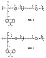
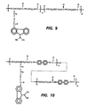
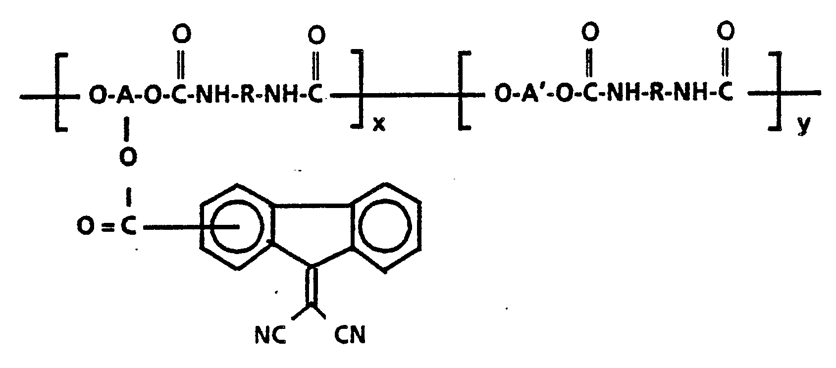
- photoresponsive imaging members having incorporated therein as charge-blocking layers polyurethanes of the formula wherein A is a trivalent group such as dimethylene alkyl group, or triethylene amine; A′ is a bivalent group such as alkylene, arylene, polyether segments, and the derivatives thereof; R is alkylene, arylene, or derivatives thereof; and x and y are number mole fractions of which the sum thereof is equal to 1. More specifically, x and y are mole fractions of from 0.05 to about 0.95.
- polyurethanes selected as the charge-blocking layer include those as represented by the following Formulas I, II and III: wherein A is a trivalent group; R is a bivalent group such as alkylene, arylene, substituted alkylene or substituted arylene group such as methylene, dimethylene, trimethylene, tetramethylene, phenylene, tolylene, and the like; R′ is an alkyl, or substituted alkyl substituent, an aryl or substituted aryl substituent; x and y represent number mole fractions of from about 0.05 to about 0.95, subject to the provision that the sum of x + y is equal to 1.0; and m and n are positive integers of from 1 to 20.
- A is a trivalent group
- R is a bivalent group such as alkylene, arylene, substituted alkylene or substituted arylene group such as methylene, dimethylene, trimethylene, tetramethylene, phenylene, tolylene, and
- alkyl substituents include those with from 1 to 25 carbon atoms, such as methyl, ethyl, propyl, butyl, pentyl, dodecyl, and the like; while examples of aryl substituents are those with from 6 to 24 carbon atoms, such as phenyl and naphthyl.
- examples of polyurethane polymers selected for the imaging members of the present invention include those represented by the formulae illustrated in Figures 1 to 10, wherein the substituents such as x and y are as defined herein.
- the polyurethanes of the present invention can be synthesized, reference Reaction Scheme 1 that follows, by the reaction of the dihydroxy-functionalized monomer (1a) and a diol (2) such as ethylene glycol, diethylene glycol, octanediol, and the like, with a slight excess of diisocyanate (3), in an inert reaction solvent medium at a temperature usually below 100°C, and preferably between 50°C to 85°C.
- a suitable catalyst such as tertiary amines, dibutyltin diacetate or dibutyltin dilaurate, can be employed to increase the rate of polymerization.
- Suitable solvents for the above polymerization reaction include ethyl acetate, tetrahydrofuran, dioxane, dimethyl sulfoxide, dimethyl acetamide, and dimethylformamide. Also, the aforesaid reaction is generally accomplished in a period of from 2 to 24 hours depending on the nature of the reagents and reaction conditions.
- diisocyanates that may be selected for the preparation of the copolyurethanes include methane diisocyanate, 1,2-ethane diisocyanate, 1,3-propane diisocyanate, 1,6-hexane diisocyanate, 1,4-cyclohexane diisocyanate, 1,4-dimethylenecyclohexane diisocyanate, benzene diisocyanate, toluene diisocyanates, methylene bis(4-phenyl isocyanate), and the like.
- dihydroxy-functionalized monomer (1a) selected for the preparation of the polyurethanes include
- the polyurethanes illustrated herein and synthesized, for example, in accordance with the processes specified can be characterized by various analytical techniques including spectroscopy, GPC, vapor pressure osmometry, and the like.
- the polyurethane can be applied to the imaging members disclosed herein in a desired thickness.
- the thickness of this layer is from 0.01 to 2 ⁇ m, and preferably from 0.1 to 2 ⁇ m.
- a photoresponsive imaging member of the present invention comprised of an optional support substrate 1, such as of aluminum; a ground plane layer 3 of a thickness of from 0.1 to 150 ⁇ m of, for example, a copper iodide, or a carbon black dispersion in a suitable binder such as poly(vinyl fluoride), polyesters, and the like; a charge-blocking polyurethane layer 5 of the formulae illustrated herein of a thickness of from 0.001 to 25 ⁇ m, and preferably 0.1 to 3 ⁇ m; an optional adhesive layer 6 of a thickness of from 0.001 to 0.5 ⁇ m; a photogenerator layer 7 of a thickness of 0. 1 to 2 ⁇ m; and a charge-transport layer 9 of a thickness of from 5 to 50 ⁇ m dispersed in an inactive resinous binder 11.
- an optional support substrate 1 such as of aluminum
- a ground plane layer 3 of a thickness of from 0.1 to 150 ⁇ m of, for example, a copper iodide,
- a photoresponsive imaging member of the present invention comprised of a polymeric substrate 15; a ground plane layer 17 comprised of copper iodide of a thickness of about 0.05 ⁇ m; a blocking layer 19 of a thickness of 0.3 ⁇ m comprised of the polyurethane of Figure 3 illustrated herein, and derived from the polycondensation of 2,2-bis(hydroxymethyl)butyl 9-dicyanomethylene-fluorene-4-carboxylate and t-butyl bis(2-hydroxyethyl)amine with toluene diisocyanates; an adhesive layer 20 comprised of a polyester, such as PE49000 available from Goodyear Chemical, phenoxy resins, silicon polymers, vinyl polymers, and the like of a thickness of 0.05 ⁇ m; a photogenerator layer 21 comprised of trigonal selenium of a thickness of 0.8 ⁇ m; and an aryl amine hole-transport layer 23 of thickness of 30 ⁇ m comprised of
- the support substrate layers may be comprised of any suitable material having the requisite mechanical properties.
- the substrate layers usually of a thickness of from 50 to 5,000 ⁇ m, may be comprised of a layer of polymeric materials such as the commercially available 'Mylar' (trademark), polyesters, polyurethanes, polyamides, and the like.
- the substrate may be flexible or rigid, and may be of a number of many different configurations such as, for example, a plate, a cylindrical drum, a scroll, an endless flexible belt, and the like.
- the substrate is in the form of an endless flexible belt or a rigid drum.
- the photoconductive or photogenerating layers of the imaging members of the present invention can be comprised of known photoconductive materials usually of a thickness of from 5 to 35 ⁇ m including, for example, amorphous selenium, amorphous selenium alloys, halogen-doped amorphous selenium, halogen-doped amorphous selenium alloys, trigonal selenium, selenide and carbonates with trigonal selenium, reference US-A-4,232,102 and 4,233,283; cadmium sulfide, cadmium selenide, cadmium telluride, cadmium sulfur selenide, cadmium sulfur telluride, cadmium seleno telluride, copper and chlorine-doped cadmium sulfide, and the like.
- Alloys of selenium included within the scope of the present invention are selenium tellurium alloys, selenium arsenic alloys, selenium tellurium arsenic alloys, and preferably such alloys containing selenium in an amount of from 70 to 99.5 percent by weight and an optional halogen material, such as chlorine, in an amount of from 50 to 200 parts per million.
- this layer can be comprised of metal phthalocyanines, metal-free phthalocyanines, reference US-A-4,265,990; other known phthalocyanines, as disclosed in US-A-3,816,118; vanadyl phthalocyanine, squaraines, perylenes, and the like.
- ground plane layers examples include inorganic materials such as, for example, aluminum, chromium, nickel, brass, copper iodide, and the like; conductive polymer materials such as aluminized Mylar; or carbon black impregnated polymer films.
- the transport layer comprises aryl amine molecules of the formula dispersed in a highly insulating and transparent organic resinous material such as polycarbonates and the like as illustrated in, for example, the '132 patent, wherein X is alkyl or halogen, preferably methyl or chlorine.
- the charge-transport layer is substantially nonabsorbing in the spectral region of intended use, that is, visible light, but is "active" in that it allows injection of photogenerated holes from the charge generator layer.
- the resin becomes electrically active when it contains from about 10 to 75 weight percent of the substituted N,N,N′,N′-tetraphenylbenzidine corresponding to the foregoing formula.
- Compounds corresponding to this formula include, for example, N,N′-diphenyl-N,N′-bis-(alkylphenyl)benzidine, wherein the alkyl is methyl, ethyl, propyl, butyl, hexyl, N,N′-diphenyl-N,N′-bis(3-methylphenyl)benzidene; N,N′-diphenyl-N,N′-bis(3-methylphenyl)1,1′-biphenyl-4,4′-diamine; and the like. With halogen substitution, the compound is N,N′-diphenyl-N,N′-bis(halophenyl)benzidene.
- electrically active small molecules which can be dispersed in the electrically inactive resin to form a layer which will transport holes include triphenylamine, bis-(4-diethylamino-2-methylphenyl)phenyl methane, and bis-(4-diethylaminophenyl)phenylmethane.
- the imaging members of the present invention inclusive of enabling the generation of images with excellent resolution, and no background deposits for an extended number of imaging cycles exceeding, for example 200,000; and moreover, the members, especially seamless photoresponsive members with the carbon black impregnated transparent ground planes, can be irradiated from behind the polyurethane ground plane, thus providing certain enabling architectural advantages such as permitting the incorporation of an erase lamp inside the photoreceptor loops. Furthermore, the addition of a charge-blocking layer in combination with the polyurethane blocking layer improves the acceptance potential while effectively reducing the dark conductivity of the imaging members, thus enabling the members to achieve acceptable desirable contrast potentials easily with relatively low or no background deposits.
- the presence of the blocking layer also enhances the resistance of the imaging members to environmental changes, such as changes in humidity and temperature. These changes generally have an adverse effect on the electrical performance of photoresponsive imaging members, giving rise to high dark conductivity and high residual potentials. These undesired electrical effects usually result in poor copy quality such as faint images with high backgrounds. Also, the sensitivity of the imaging member to humidity and temperature would render the copy quality dependent on the environmental conditions.
- imaging and printing processes wherein, for example, an electrostatic latent image is generated on the imaging members illustrated herein subsequently rendering the image visible with a developer composition comprised of a toner with resin particles such as styrene polymers, pigment particles such as carbon black, charge-enhancing additives such as cetyl pyridinium chloride, external additives such as colloidal silicas and metal salts, and metal salts of fatty acids inclusive of zinc stearate, reference for example US-A-4,298,672; 4,338,390; 4,560,635; 3,590,000; 3,900,588, and 3,983,045; thereafter transferring the developed image to a suitable substrate such as paper; and permanently affixing the image thereto by, for example, heat or other similar processes.
- resin particles such as styrene polymers, pigment particles such as carbon black
- charge-enhancing additives such as cetyl pyridinium chloride
- external additives such as colloidal silicas and metal salts
- a mixture of 0.030 mole of diol monomer (a), 0.030 mole of diethylene glycol, 0.063 mole of toluene diisocyanates (mixture of 2,4- and 2,6-diisocyanates), and 0.05 gram of dibutyltin dilaurate was dissolved in 100 milliliters of dried dimethyl sulfoxide.
- the mixture was heated under an inert atmosphere at 70 to 75°C for 4 hours, after which 5 milliliters of ethanol were added. Thereafter, the reaction mixture was heated for another hour before cooling down to room temperature. This mixture was then poured slowly into 3 liters of swirling methanol to precipitate the resultant polyurethane.
- the polyurethane product was filtered and washed twice with 500 milliliters of methanol.
- the yield of the above copolyurethane with the formula as represented by Figure 1 was 86 percent after drying in vacuo at 65°C for 24 hours; DP (degree of polymerization) was 103; Tg 121°C (midpoint); IR (KBr) 1,729; 2,221 cm ⁇ 1.
- the copolyurethane of Figure 1 above was prepared according to the procedure of Example IV with the exceptions that 0.036 mole of diol monomer (a), 0.024 mole of diethylene glycol, and 0.063 mole of toluene diisocyanates were employed; and the reaction was conducted for 6 hours.
- the yield was 88 percent; DP 112; and Tg 134°C; IR (KBr) 1,730; 2,221 cm ⁇ 1.
- the precipitate was filtered, washed with methanol, and dried in vacuo at 60°C for 24 hours.
- the yield of the above copolyurethane was 91 percent; DP 121; and Tg 134°C; IR (KBr) 1,730; 2,222 cm ⁇ 1.
- the synthesis of the above copolyurethane was accomplished in accordance with the procedure of Example VI with a mixture of 0.030 mole of diol monomer (a), 0.030 mole of 1,8-octanediol, 0.063 mole of toluene diisocyanates, and 0.05 gram of dibutyltin dilaurate.
- the yield of the above copolyurethane was 84 percent; DP 99; Tg 118°C; IR (KBr) 1,730; 2,222 cm ⁇ 1.
- the first member was comprised of a six-layer structure with a configuration as illustrated in Figure 11, and the second a five-layer structure without the polyurethane blocking layer to serve as a control device.
- the conductive ground planes comprised of commercially available cuprous iodide were fabricated as follows: a saturated solution of cuprous iodide in butyronitrile was prepared by agitating 2.3 grams of ultra pure cuprous iodide in 100 milliliters of butyronitrile for 4 to 16 hours, followed by filtering through a filter of 0.4 ⁇ m porosity. The clear filtrate was coated by drawbar technique onto a 'Mylar' substrate using a 150 ⁇ m bar gap. Subsequently, the ground plane coating was dried in an air convection oven at 100°C for 10 minutes. The dry thickness of the coating was about 0.5 ⁇ m.
- the upper four layers, reference Figure 11, were coated from appropriate solutions using the above described known drawbar technique. Except for the top transport layer, each coating was dried for one hour before the subsequent layer was coated.
- the blocking layer of a thickness of 0.25 ⁇ m was prepared from a solution of 0.15 gram of the copolyurethane of Figure 1 in 10 milliliters of tetrahydrofuran, and was coated at a thickness of about 0.2 ⁇ m using 12 ⁇ m bar gap.
- Overcoated on top of the blocking layer was a 0.06 ⁇ m thick adhesive layer which was obtained from a solution of 0.12 gram of Reillen 4200 poly(vinyl pyridine) in 20 milliliters of isobutanol and 2 milliliters of isopropanol.
- the photogenerating layer of trigonal selenium was obtained by coating a dispersion of 28.5 parts of trigonal selenium, 16 parts of N,N′-diphenyl-N,N′-bis(3-methylphenyl)-benzidine, 55.5 parts of poly(vinyl carbazole) in a mixture of tetrahydrofuran and toluene.
- the top transport layer of a thickness of 25 ⁇ m was prepared from a solution of 40 parts of N,N′-diphenyl-N,N′-bis(3-methylphenyl)benzidine and 60 parts of 'Makrolon' (trademark) polycarbonate in methylene chloride. The transport layer coating was dried at 50°C for 30 minutes, and then at 110°C for another 10 minutes.
- a photoresponsive imaging device comprising a five-layer structure with a conductive substrate as a ground plane was fabricated by essentially repeating the procedure of Example X.
- the conductive substrate was a 75 ⁇ m thick carbon black impregnated thermoplastic sheet available commercially from E.I. Dupont De Nemours, Inc.
- the thermoplastic was poly(vinyl fluoride) with a loading of carbon black dispersion of about 25 percent.
- the resistivity of this ground plane was 104 ohms/square.
- a blocking layer of thickness of about 0.8 ⁇ m was coated on the ground plane in accordance with the procedure of Example X, except that the copolyurethane of Figure 2 was selected in place of the copolyurethane of Figure 1.
- On top of the blocking layer was coated in succession a photogenerating layer, and a transport layer which were identical to those of Example X.
- a control imaging device without the blocking layer was also fabricated by repeating the aforementioned process.
- the members were then electrically tested in a cyclic scanner for over 200 cycles.
- the scanner was equipped with a single wire corotron set to deposit 9x10 ⁇ 8 coulombs/cm2 of charge on the imaging surface.
- the imaging devices were wrapped around an aluminum drum with a circumference of 765 mm, and rotated at a speed of 12 rpm, giving a surface speed of 150 mm per second.
- the devices were discharged with a tungsten white light source.
- the device with a blocking layer exhibited stable acceptance for over 200 cycles, and the residual potential remained at 30 to 50 volts.
- the acceptance potential of the control device was considerably lower and unstable after 200 cycles of charging and discharging, reference the following table.
- a photoresponsive imaging member similar to Example X was prepared by repeating the procedure of this Example with a 'Mylar' substrate, an eight- ⁇ m thick conductive layer comprising 15 percent of carbon black (Black Pearls 2000 available from Cabot Corporation) in polyester PE-49000 (from Dupont), a blocking layer of the copolyurethane of Figure 3, an adhesive layer, a photogenerating layer, and a transport layer identical to those of Example X.
- the solution for the conductive layer was prepared by dispersing by agitation 0.94 gram of carbon black in a solution of 5.32 grams of polyester PE-49000 in 325 milliliters of methylene chloride.
- the device was electrically tested by repeating the procedure of Examples X and XI, and substantially similar results were obtained.
- a photoresponsive imaging member similar to that of Example XII was prepared by repeating the procedure of this Example with the exception that a ball grained aluminum plate was employed as the conductive layer instead of the carbon black impregnated polyester film. Electrical testing of the device was accomplished by repeating the procedure of Example X. Substantially similar results were obtained.
- a photoresponsive imaging member similar to that of Example X was prepared by repeating the procedure of this Example with the exception that a polypyrrole conductive coating was used instead of cuprous iodide.
- the polypyrrole conductive layer was prepared by coating a 5 percent solution of ICP-117 polypyrrole dispersion (from Polaroid Corporation) using a drawbar with a 50 ⁇ m gap opening. The coating was dried as before at 100°C for 10 minutes. Electrical testing was accomplished in accordance with the procedure of Example X, and substantially similar results were obtained.
Abstract

Description
- This invention is generally directed to imaging members, and more specifically the present invention relates to the selection of certain polyurethanes which function as charge-blocking layers for photoresponsive imaging members, especially seamless organic imaging members. In one embodiment, the present invention relates to an imaging member comprised of a support substrate, a conductive ground plane, a charge-blocking layer comprised of a urethane polymer, an adhesive layer, a photogenerator, and a charge-transport layer. In another embodiment of the present invention, there are provided seamless imaging members comprised of a hole-transport layer, a photogenerating layer, an adhesive layer, a hole-blocking layer comprised of a urethane polymer, and a conductive support substrate. The aforementioned imaging members are useful in electrophotographic printing and imaging processes, and in particular, can be selected for the generation of latent images in electrostatic imaging systems. With further regard to the imaging members of the present invention, the primary function of the hole-blocking layer is to prevent dark injection of charge carriers from the ground plane or conductive substrate into the photogenerating layer, thus significantly reducing the dark decay characteristics of imaging members.
- Layered imaging members with blocking layers are known, especially those wherein the blocking layer is comprised of a metal oxide, or a siloxane, reference US-A-4,464,450.
- Illustrated in US-A-4,562, 132, are imaging members comprised of a support substrate, a hole-transport layer comprised of an aryl amine hole-transport compound dispersed in an inactive resinous binder, a photogenerating layer comprised of a photogenerating pigment optionally dispersed in a resinous binder, and as a protective topcoating, an electron-transport compound of the following formula dispersed in a resinous binder

- Moreover, illustrated in US-A-4 835 081 are inorganic photoresponsive imaging members having incorporated therein as protective overcoatings polycondensation polymers derived from the polycondensation of 2,2-bis(hydroxymethyl)-butyl 9-dicyanomethylenefluorene-4-carboxylate, and diisocyanate. Also disclosed in the copending application are layered photoresponsive imaging members comprised of a supporting substrate, a photoconductive layer, an arylamine hole-transport layer, and a protective overcoating layer comprised of the aforementioned polyurethane polymers. In addition, the polyurethane polymers of the copending application are useful as the top overcoating for positive-charging layered photoresponsive devices comprised of a supporting substrate, a hole-transport layer, and a photoconductive layer, and wherein the polymers are of the following formula

- The polyurethanes of the present invention are somewhat similar to the aforementioned polyurethane coatings. More specifically, the polyurethanes of the present invention contain therein certain highly flexible segments, thereby providing the desired flexibility characteristic useful for application in belt-type imaging devices. Furthermore, the presence of the soft flexible segments in the polyurethanes of the present invention greatly improves their solubilities in common coating solvents such as aromatic hydrocarbons, tetrahydrofuran, chlorinated hydrocarbons, and the like, thereby enabling the coating process to be accomplished in a variety of solvents by different coating techniques, such as dip coating, spray coating, and the like. More importantly, the incorporation of the flexible segments into the polyurethane structure renders the synthesis of higher molecular-weight polyurethanes feasible, thus affording mechanically strong and highly durable polyurethane blocking layers. The polyurethanes of the present invention also display good adhesion properties, thereby improving the adhesion of the generator layer to the ground plane.
- In US-A-4 820 601 are illustrated imaging members with protective overcoatings comprised of the copolyurethanes selected as blocking layers for the same, or similar imaging members of the present invention.
- There are disclosed in US-A-4,474,865 improved photoresponsive imaging members with electron-transporting components containing specific dicyano fluoro ester moieties; 3,928,034, which illustrates the incorporation of electron transporting moieties chemically attached to polymers,
reference columns 7 and 8; and 4,007,043; 4,063,947; 4,075,012; and 3,896,184. Also of interest are US-A-3,108,092; 3,451,969; 4,063,947; and 4,203,764; and NL-A-7606525. Of particular interest are US-A-and NL-A-7606525, which disclose imaging members with electron-transport compounds,reference column 3, line 57, to column 4,line 30, of the ′947 patent; US-A-3,907,650, which discloses hole-transport materials for an electron-blocking layer,reference column 3; 3,975,635, which discloses a xeroradiographic plate with a conductive backing member, an overlayer of selenium, and an intermediate layer of polyvinyl carbazole or an alloy of arsenic and selenium; 4,582,773 illustrating electrophotographic photoreceptors including a blocking layer formed from a doped microcrystalline semiconductor alloy; and US-A-4,013,623; 4,050,934, which disclose a dicyanomethylene group as the electrical active moiety for use in electron-transporting layers. Other patents of background interest are US-A-4,657,751, which mentions cuprous iodide as a conductive substrate film; 2,901,348; 3,713,821; 3,879,199; 3,888,665; 3,891,435; 3,972,717; 4,010,031; 4,082,551; 4,106,935; 4,391,888; and 4,415,639. - While the above-described imaging members are suitable for their intended purposes, there continues to be a need for layered photoresponsive imaging members with functionally superior charge-blocking layers. More specifically, there continues to be a need for charge-blocking layers which can effectively block the dark injection of charge carriers from the ground plane into the photogenerating layer. Additionally, there continues to be a need for charge-blocking layers with excellent flexibility characteristics, thereby enabling their use in belt-type organic imaging members. Furthermore, there is a need for organic charge-blocking layer materials which are soluble in a variety of solvents thereby permitting improved coatability, and allowing economical spray and dip coating processes to be selected for the preparation thereof. Another need resides in the provision of charge-blocking layers with acceptable desirable adhesive properties enabling the layer to adhere to the ground plane or conductive substrate, thereby improving the overall layered lamination integrity of the imaging members.
- It is an object of the present invention to provide an improved photoresponsive imaging member.
- Accordingly the present invention provides photoresponsive imaging members having incorporated therein as charge-blocking layers certain polyurethanes as claimed in the appended claims. The polyurethanes which are the subject-matter of this invention are illustrated in the accompanying drawings.
- More specifically, in one embodiment of the present invention there are provided photoresponsive imaging members having incorporated therein as charge-blocking layers polyurethanes of the formula

- Examples of polyurethanes selected as the charge-blocking layer include those as represented by the following Formulas I, II and III:

- Specifically, examples of polyurethane polymers selected for the imaging members of the present invention include those represented by the formulae illustrated in Figures 1 to 10, wherein the substituents such as x and y are as defined herein.
- The polyurethanes of the present invention can be synthesized,
reference Reaction Scheme 1 that follows, by the reaction of the dihydroxy-functionalized monomer (1a) and a diol (2) such as ethylene glycol, diethylene glycol, octanediol, and the like, with a slight excess of diisocyanate (3), in an inert reaction solvent medium at a temperature usually below 100°C, and preferably between 50°C to 85°C. In general, a suitable catalyst, such as tertiary amines, dibutyltin diacetate or dibutyltin dilaurate, can be employed to increase the rate of polymerization.
- Examples of suitable solvents for the above polymerization reaction include ethyl acetate, tetrahydrofuran, dioxane, dimethyl sulfoxide, dimethyl acetamide, and dimethylformamide. Also, the aforesaid reaction is generally accomplished in a period of from 2 to 24 hours depending on the nature of the reagents and reaction conditions.
- Examples of diisocyanates that may be selected for the preparation of the copolyurethanes include methane diisocyanate, 1,2-ethane diisocyanate, 1,3-propane diisocyanate, 1,6-hexane diisocyanate, 1,4-cyclohexane diisocyanate, 1,4-dimethylenecyclohexane diisocyanate, benzene diisocyanate, toluene diisocyanates, methylene bis(4-phenyl isocyanate), and the like.
- Specific examples of the dihydroxy-functionalized monomer (1a) selected for the preparation of the polyurethanes include


- The polyurethanes illustrated herein and synthesized, for example, in accordance with the processes specified can be characterized by various analytical techniques including spectroscopy, GPC, vapor pressure osmometry, and the like. Also, the polyurethane can be applied to the imaging members disclosed herein in a desired thickness. Generally, the thickness of this layer is from 0.01 to 2 µm, and preferably from 0.1 to 2 µm.
- The invention will now be illustrated with reference to specific preferred embodiments shown in the drawings, wherein
- Figures 1 through 10 are formulas representing polyurethanes charge-blocking layers for the imaging members of the present invention;
- Figure 11 represents a cross-sectional view of a photoresponsive imaging member of the present invention; and
- Figure 12 represents a cross-sectional view of a preferred photoresponsive imaging member of the present invention.
- There is illustrated in Figure 11 a photoresponsive imaging member of the present invention comprised of an
optional support substrate 1, such as of aluminum; aground plane layer 3 of a thickness of from 0.1 to 150 µm of, for example, a copper iodide, or a carbon black dispersion in a suitable binder such as poly(vinyl fluoride), polyesters, and the like; a charge-blockingpolyurethane layer 5 of the formulae illustrated herein of a thickness of from 0.001 to 25 µm, and preferably 0.1 to 3 µm; an optionaladhesive layer 6 of a thickness of from 0.001 to 0.5 µm; aphotogenerator layer 7 of a thickness of 0. 1 to 2 µm; and a charge-transport layer 9 of a thickness of from 5 to 50 µm dispersed in an inactiveresinous binder 11. - Illustrated in Figure 12 is a photoresponsive imaging member of the present invention comprised of a
polymeric substrate 15; aground plane layer 17 comprised of copper iodide of a thickness of about 0.05 µm; ablocking layer 19 of a thickness of 0.3 µm comprised of the polyurethane of Figure 3 illustrated herein, and derived from the polycondensation of 2,2-bis(hydroxymethyl)butyl 9-dicyanomethylene-fluorene-4-carboxylate and t-butyl bis(2-hydroxyethyl)amine with toluene diisocyanates; anadhesive layer 20 comprised of a polyester, such as PE49000 available from Goodyear Chemical, phenoxy resins, silicon polymers, vinyl polymers, and the like of a thickness of 0.05 µm; aphotogenerator layer 21 comprised of trigonal selenium of a thickness of 0.8 µm; and an aryl amine hole-transport layer 23 of thickness of 30 µm comprised of adiamine 24 such as N,N′-diphenyl-N,N′- bis(3-methyl phenyl) 1,1′-biphenyl-4,4′-diamine dispersed in an inactiveresinous binder 25. - With further reference to the photoresponsive imaging members illustrated herein, and particularly with reference to Figures 11 to 12, the support substrate layers may be comprised of any suitable material having the requisite mechanical properties. Thus, the substrate layers, usually of a thickness of from 50 to 5,000 µm, may be comprised of a layer of polymeric materials such as the commercially available 'Mylar' (trademark), polyesters, polyurethanes, polyamides, and the like. The substrate may be flexible or rigid, and may be of a number of many different configurations such as, for example, a plate, a cylindrical drum, a scroll, an endless flexible belt, and the like. Preferably, the substrate is in the form of an endless flexible belt or a rigid drum.
- The photoconductive or photogenerating layers of the imaging members of the present invention, reference for example the members of Figures 11 and 12, can be comprised of known photoconductive materials usually of a thickness of from 5 to 35 µm including, for example, amorphous selenium, amorphous selenium alloys, halogen-doped amorphous selenium, halogen-doped amorphous selenium alloys, trigonal selenium, selenide and carbonates with trigonal selenium, reference US-A-4,232,102 and 4,233,283; cadmium sulfide, cadmium selenide, cadmium telluride, cadmium sulfur selenide, cadmium sulfur telluride, cadmium seleno telluride, copper and chlorine-doped cadmium sulfide, and the like. Alloys of selenium included within the scope of the present invention are selenium tellurium alloys, selenium arsenic alloys, selenium tellurium arsenic alloys, and preferably such alloys containing selenium in an amount of from 70 to 99.5 percent by weight and an optional halogen material, such as chlorine, in an amount of from 50 to 200 parts per million. Also, this layer can be comprised of metal phthalocyanines, metal-free phthalocyanines, reference US-A-4,265,990; other known phthalocyanines, as disclosed in US-A-3,816,118; vanadyl phthalocyanine, squaraines, perylenes, and the like.
- Examples of known ground plane layers include inorganic materials such as, for example, aluminum, chromium, nickel, brass, copper iodide, and the like; conductive polymer materials such as aluminized Mylar; or carbon black impregnated polymer films.
- Various hole-transport layer compositions can be selected providing these substances are capable of transporting holes, this layer generally having a thickness in the range of from 5 to 50 µm, and preferably from 20 to 40 µm. Thus, the transport layer comprises aryl amine molecules of the formula

- Other electrically active small molecules which can be dispersed in the electrically inactive resin to form a layer which will transport holes include triphenylamine, bis-(4-diethylamino-2-methylphenyl)phenyl methane, and bis-(4-diethylaminophenyl)phenylmethane.
- Several advantages are associated with the imaging members of the present invention inclusive of enabling the generation of images with excellent resolution, and no background deposits for an extended number of imaging cycles exceeding, for example 200,000; and moreover, the members, especially seamless photoresponsive members with the carbon black impregnated transparent ground planes, can be irradiated from behind the polyurethane ground plane, thus providing certain enabling architectural advantages such as permitting the incorporation of an erase lamp inside the photoreceptor loops. Furthermore, the addition of a charge-blocking layer in combination with the polyurethane blocking layer improves the acceptance potential while effectively reducing the dark conductivity of the imaging members, thus enabling the members to achieve acceptable desirable contrast potentials easily with relatively low or no background deposits. The presence of the blocking layer also enhances the resistance of the imaging members to environmental changes, such as changes in humidity and temperature. These changes generally have an adverse effect on the electrical performance of photoresponsive imaging members, giving rise to high dark conductivity and high residual potentials. These undesired electrical effects usually result in poor copy quality such as faint images with high backgrounds. Also, the sensitivity of the imaging member to humidity and temperature would render the copy quality dependent on the environmental conditions.
- With further respect to the present invention, there are envisioned imaging and printing processes wherein, for example, an electrostatic latent image is generated on the imaging members illustrated herein subsequently rendering the image visible with a developer composition comprised of a toner with resin particles such as styrene polymers, pigment particles such as carbon black, charge-enhancing additives such as cetyl pyridinium chloride, external additives such as colloidal silicas and metal salts, and metal salts of fatty acids inclusive of zinc stearate, reference for example US-A-4,298,672; 4,338,390; 4,560,635; 3,590,000; 3,900,588, and 3,983,045; thereafter transferring the developed image to a suitable substrate such as paper; and permanently affixing the image thereto by, for example, heat or other similar processes.
- The invention will now be described in detail with respect to specific preferred embodiments thereof, it being understood that these examples are intended to be illustrative only and the invention is not intended to be limited to the materials, conditions, and process parameters recited herein. All percentages and parts are by weight unless otherwise indicated.
- A mixture of 2.1 kilograms of trimethylolpropane, 173 grams of fluorenone-4-carboxylic acid, and 8 milliliters of sulfuric acid was mechanically stirred and heated in a 5-liter flask at 100°C for 5 hours. The mixture was cooled to about 80°C, and 1 liter of methanol was added. Thereafter, the resulting solution was poured slowly into 17 liters of 3 percent aqueous sodium bicarbonate solution with constant stirring, and the crude product resulting was filtered, washed several times with water, and dried. Purification by recrystallization from ethyl acetate afforded 187 grams of pure 2,2-bis(hydroxymethylbutyl) fluorenone-4-carboxylate, m.p., 134 to 135.5°C.
- A solution of 240 grams of the ester as obtained above, 93 grams of malononitrile, and 5 milliliters of piperidine in 2.3 liters of absolute methanol was heated under reflux in a nitrogen atmosphere for 5 hours. After the reaction, the mixture was cooled to about 50°C, and the solid product was filtered'. The product obtained of Formula (a) was washed twice with methanol, dried in vacuo at 100°C to afford 229 grams of pure (a), m.p., 208 to 209°C.
Analysis Calculated for C₂₃H₂₀N₂O₄: C,71.12; H, 5.19; N, 7.12 Found: C,71.23; H, 5.21; N, 7.13 IR (KBr), cm⁻¹: 3,420; 2,230; 1,730. ¹H MNR (DMSO-d₆), ppm: 0.85 (t, 3H); 1.4 (q, 2H); 3.4 (d, 4H); 4.3 (s, 2H); 4.4 (t, 2H); 7.4 to 8.6 (m, 7H). - A solution of 30.0 grams of phloroglucinol and 70 milliliters of pyridine in 300 milliliters of dichloromethane was stirred at room temperature under a nitrogen atmosphere. Thereafter, a solution of 8.0 grams of (4-chloroformyl-9-fluorenylidene)malononitrile in 400 milliliters of dichloromethane was added thereto over a period of 1 hour. After addition, the reaction mixture was further stirred for another hour. The mixture was washed three times with dilute aqueous HCl solution, twice with dilute aqueous NaHCO₃ solution, and once with water. The solution was dried, filtered, and evaporated under reduced pressure to give the crude product. Recrystallization from methanol afforded 6.1 grams of (b), m.p., 255.5 to 257°C.
Analysis Calculated for C₂₃H₁₂N₂O₄: C,72.63; H,3.18; N,7.37 Found: C,72.41; H,3.12; N,7.17 IR (KBr), cm⁻¹: 3,410; 2,230; 1,730. ¹H MNR (acetone-d₆), ppm: 3.25 (br s, 2H); 6.8 (s, 3H); 7.6 to 9.0 (m, 7H). - A solution of 100.0 grams of triethanolamine and 58 milliliters of dry pyridine in 350 milliliters of dry dichloromethane was stirred at room temperature under a nitrogen atmosphere. Thereafter, a solution of 8.0 grams of (4-chloroformyl-9-fluorenylidene)malononitrile in 400 milliliters of dry dichloromethane was added over a period of 1 hour. After addition, the reaction mixture was further stirred for another hour. The reaction mixture was washed several times with water to remove the excess amines and the corresponding hydrochloride salts, dried with anhydrous magnesium sulfate, and filtered. Evaporation of the filtrate provided 5 grams of crude product. Purification by recrystallization from isopropanol afforded 4.5 grams of pure (c), m.p., 155.5 to 156.5°C.
Analysis Calculated for C₂₃H₂₁N₃O₄: C,68.48; H,5.25; N,10.42 Found: C,68.31; H,5.33; N,10.35 IR (KBr), cm⁻¹: 3,360; 2,225; 1,730. ¹H MNR (DMSO-d₆), ppm: 2.6 (t, 4H); 2.8 (t, 2H); 3.25 (br s, 2H); 3.4 (t, 4H); 4.4 (t, 2H); 7.4 to 8.6 (m, 7H). - Other hydroxy carboxylates can be prepared in a manner similar to Examples I and III.
- A mixture of 0.030 mole of diol monomer (a), 0.030 mole of diethylene glycol, 0.063 mole of toluene diisocyanates (mixture of 2,4- and 2,6-diisocyanates), and 0.05 gram of dibutyltin dilaurate was dissolved in 100 milliliters of dried dimethyl sulfoxide. The mixture was heated under an inert atmosphere at 70 to 75°C for 4 hours, after which 5 milliliters of ethanol were added. Thereafter, the reaction mixture was heated for another hour before cooling down to room temperature. This mixture was then poured slowly into 3 liters of swirling methanol to precipitate the resultant polyurethane. The polyurethane product was filtered and washed twice with 500 milliliters of methanol. The yield of the above copolyurethane with the formula as represented by Figure 1 was 86 percent after drying in vacuo at 65°C for 24 hours; DP (degree of polymerization) was 103; Tg 121°C (midpoint); IR (KBr) 1,729; 2,221 cm⁻¹.
- The copolyurethane of Figure 1 above was prepared according to the procedure of Example IV with the exceptions that 0.036 mole of diol monomer (a), 0.024 mole of diethylene glycol, and 0.063 mole of toluene diisocyanates were employed; and the reaction was conducted for 6 hours. The yield was 88 percent; DP 112; and Tg 134°C; IR (KBr) 1,730; 2,221 cm⁻¹.
- A mixture of 0.150 mole of diol monomer (a), 0.150 mole of t-butyl bis(2-hydroxyethylamine), and 0.316 mole of tolylene diisocyanates, and 0.2 gram of dibutyltin dilaurate in 700 milliliters of dried dimethylsulfoxide was heated under a nitrogen atmosphere at 70 to 75°C for 10 hours. Subsequently, 10 milliliters of absolute ethanol was added and the reaction was continued at the same temperature for another hour. After cooling down to room temperature, the reaction mixture was poured into 5 liters of methanol to precipitate the above polyurethane product. The precipitate was filtered, washed with methanol, and dried in vacuo at 60°C for 24 hours. The yield of the above copolyurethane was 91 percent; DP 121; and Tg 134°C; IR (KBr) 1,730; 2,222 cm⁻¹.
- The synthesis of the above copolyurethane was accomplished in accordance with the procedure of Example VI with a mixture of 0.030 mole of diol monomer (a), 0.030 mole of 1,8-octanediol, 0.063 mole of toluene diisocyanates, and 0.05 gram of dibutyltin dilaurate. The yield of the above copolyurethane was 84 percent; DP 99; Tg 118°C; IR (KBr) 1,730; 2,222 cm⁻¹.
- The synthesis of the above copolyurethane was accomplished in accordance with the procedure of Example IV with monomer (c), 1,5-pentanediol and toluene diisocyanates except that the reaction was conducted in dry dimethylformamide. The yield of the above copolyurethane was 92 percent; DP 103; Tg 107°C; IR (KBr) 1,730; 2,222 cm⁻¹.
- The synthesis of the above copolyurethane was accomplished in accordance with the procedure of Example V with 0.042 mole of diol monomer (b), 0.018 mole of t-butyl bis(2-hydroxyethyl)amine, 0.063 mole of 1,4-benzenediisocyanate, and 0.05 gram of dibutyltin dilaurate. The reaction was conducted in dried tetrahydrofuran, and the yield of the above copolyurethane was 87 percent; DP 89; Tg 138°C; IR (KBr) 1,730; 2,222 cm⁻¹.
- Two substantially identical photoresponsive imaging devices were fabricated as follows. The first member was comprised of a six-layer structure with a configuration as illustrated in Figure 11, and the second a five-layer structure without the polyurethane blocking layer to serve as a control device.
- The conductive ground planes comprised of commercially available cuprous iodide were fabricated as follows: a saturated solution of cuprous iodide in butyronitrile was prepared by agitating 2.3 grams of ultra pure cuprous iodide in 100 milliliters of butyronitrile for 4 to 16 hours, followed by filtering through a filter of 0.4 µm porosity. The clear filtrate was coated by drawbar technique onto a 'Mylar' substrate using a 150 µm bar gap. Subsequently, the ground plane coating was dried in an air convection oven at 100°C for 10 minutes. The dry thickness of the coating was about 0.5 µm.
- The upper four layers, reference Figure 11, were coated from appropriate solutions using the above described known drawbar technique. Except for the top transport layer, each coating was dried for one hour before the subsequent layer was coated. The blocking layer of a thickness of 0.25 µm was prepared from a solution of 0.15 gram of the copolyurethane of Figure 1 in 10 milliliters of tetrahydrofuran, and was coated at a thickness of about 0.2 µm using 12 µm bar gap. Overcoated on top of the blocking layer was a 0.06 µm thick adhesive layer which was obtained from a solution of 0.12 gram of Reillen 4200 poly(vinyl pyridine) in 20 milliliters of isobutanol and 2 milliliters of isopropanol. The photogenerating layer of trigonal selenium, about 1 µm in thickness, was obtained by coating a dispersion of 28.5 parts of trigonal selenium, 16 parts of N,N′-diphenyl-N,N′-bis(3-methylphenyl)-benzidine, 55.5 parts of poly(vinyl carbazole) in a mixture of tetrahydrofuran and toluene. The top transport layer of a thickness of 25 µm was prepared from a solution of 40 parts of N,N′-diphenyl-N,N′-bis(3-methylphenyl)benzidine and 60 parts of 'Makrolon' (trademark) polycarbonate in methylene chloride. The transport layer coating was dried at 50°C for 30 minutes, and then at 110°C for another 10 minutes.
- The two members, one with the polyurethane blocking layer, and one without, were tested electrically by negatively charging with a corotron, and discharging by exposure to a tungsten white light. The acceptance potentials of these imaging devices after charging, and their residual potentials after exposure to white light were recorded. The surface potential was measured using a wire loop probe contained in a shielded cylinder and placed directly above the surface of the imaging device. The cylinder was grounded, and the loop was capacitively coupled to the surface potential of imaging device. The following table summarizes the electrical performance of these devices, and indicates the effective blockage of charge injection by the blocking layer:
ACCEPTANCE POTENTIAL (Volts) RESIDUAL POTENTIAL (Volts) WITH POLYURETHANE BLOCKING LAYER 520 10 WITHOUT BLOCKING LAYER 20 0 - A photoresponsive imaging device comprising a five-layer structure with a conductive substrate as a ground plane was fabricated by essentially repeating the procedure of Example X.
- The conductive substrate was a 75 µm thick carbon black impregnated thermoplastic sheet available commercially from E.I. Dupont De Nemours, Inc. The thermoplastic was poly(vinyl fluoride) with a loading of carbon black dispersion of about 25 percent. The resistivity of this ground plane was 10⁴ ohms/square. A blocking layer of thickness of about 0.8 µm was coated on the ground plane in accordance with the procedure of Example X, except that the copolyurethane of Figure 2 was selected in place of the copolyurethane of Figure 1. On top of the blocking layer was coated in succession a photogenerating layer, and a transport layer which were identical to those of Example X. A control imaging device without the blocking layer was also fabricated by repeating the aforementioned process.
- The members (devices) were then electrically tested in a cyclic scanner for over 200 cycles. The scanner was equipped with a single wire corotron set to deposit 9x10⁻⁸ coulombs/cm² of charge on the imaging surface. The imaging devices were wrapped around an aluminum drum with a circumference of 765 mm, and rotated at a speed of 12 rpm, giving a surface speed of 150 mm per second. The devices were discharged with a tungsten white light source. The device with a blocking layer exhibited stable acceptance for over 200 cycles, and the residual potential remained at 30 to 50 volts. The acceptance potential of the control device was considerably lower and unstable after 200 cycles of charging and discharging, reference the following table.
ACCEPTANCE POTENTIAL (Volts) RESIDUAL POTENTIAL (Volts) 1st cycle 200th cycle 1st cycle 200th cycle WITH POLYURETHANE BLOCKING LAYER 880 920 35 50 WITHOUT BLOCKING LAYER 420 330 32 36 - A photoresponsive imaging member similar to Example X was prepared by repeating the procedure of this Example with a 'Mylar' substrate, an eight-µm thick conductive layer comprising 15 percent of carbon black (Black Pearls 2000 available from Cabot Corporation) in polyester PE-49000 (from Dupont), a blocking layer of the copolyurethane of Figure 3, an adhesive layer, a photogenerating layer, and a transport layer identical to those of Example X. The solution for the conductive layer was prepared by dispersing by agitation 0.94 gram of carbon black in a solution of 5.32 grams of polyester PE-49000 in 325 milliliters of methylene chloride. The device was electrically tested by repeating the procedure of Examples X and XI, and substantially similar results were obtained.
- A photoresponsive imaging member similar to that of Example XII was prepared by repeating the procedure of this Example with the exception that a ball grained aluminum plate was employed as the conductive layer instead of the carbon black impregnated polyester film. Electrical testing of the device was accomplished by repeating the procedure of Example X. Substantially similar results were obtained.
- A photoresponsive imaging member similar to that of Example X was prepared by repeating the procedure of this Example with the exception that a polypyrrole conductive coating was used instead of cuprous iodide. The polypyrrole conductive layer was prepared by coating a 5 percent solution of ICP-117 polypyrrole dispersion (from Polaroid Corporation) using a drawbar with a 50 µm gap opening. The coating was dried as before at 100°C for 10 minutes. Electrical testing was accomplished in accordance with the procedure of Example X, and substantially similar results were obtained.
Claims (10)
Applications Claiming Priority (2)
| Application Number | Priority Date | Filing Date | Title |
|---|---|---|---|
| US252959 | 1988-10-03 | ||
| US07/252,959 US4921769A (en) | 1988-10-03 | 1988-10-03 | Photoresponsive imaging members with polyurethane blocking layers |
Publications (3)
| Publication Number | Publication Date |
|---|---|
| EP0363078A2 true EP0363078A2 (en) | 1990-04-11 |
| EP0363078A3 EP0363078A3 (en) | 1990-07-11 |
| EP0363078B1 EP0363078B1 (en) | 1995-06-07 |
Family
ID=22958271
Family Applications (1)
| Application Number | Title | Priority Date | Filing Date |
|---|---|---|---|
| EP89309896A Expired - Lifetime EP0363078B1 (en) | 1988-10-03 | 1989-09-28 | Photoresponsive imaging members |
Country Status (4)
| Country | Link |
|---|---|
| US (1) | US4921769A (en) |
| EP (1) | EP0363078B1 (en) |
| JP (1) | JP2571284B2 (en) |
| DE (1) | DE68922955T2 (en) |
Cited By (1)
| Publication number | Priority date | Publication date | Assignee | Title |
|---|---|---|---|---|
| EP0452681A2 (en) * | 1990-04-20 | 1991-10-23 | Xerox Corporation | Systems utilizing polyarylamine polymers |
Families Citing this family (134)
| Publication number | Priority date | Publication date | Assignee | Title |
|---|---|---|---|---|
| JP2567090B2 (en) * | 1989-04-20 | 1996-12-25 | キヤノン株式会社 | Electrophotographic photoreceptor |
| US5089364A (en) * | 1990-10-26 | 1992-02-18 | Xerox Corporation | Electrophotographic imaging members containing a polyurethane adhesive layer |
| JP3317116B2 (en) * | 1995-12-21 | 2002-08-26 | 富士ゼロックス株式会社 | Electrophotographic photoreceptor |
| US6228546B1 (en) | 1997-11-19 | 2001-05-08 | Canon Kabushiki Kaisha | Polymer, electrophotographic photosensitive member containing the polymer, process cartridge and electrophotographic apparatus having the electrophotographic photosensitive member |
| US5994014A (en) * | 1998-02-17 | 1999-11-30 | Lexmark International, Inc. | Photoconductor containing silicone microspheres |
| US5874193A (en) * | 1998-07-30 | 1999-02-23 | Xerox Corporation | Photoconductive imaging members |
| US5871877A (en) * | 1998-07-30 | 1999-02-16 | Xerox Corporation | Photoconductive imaging members |
| US6132912A (en) * | 1999-05-27 | 2000-10-17 | Xerox Corporation | Photoconductive imaging members |
| US6030735A (en) * | 1999-10-12 | 2000-02-29 | Xerox Corporation | Photoconductive imaging members with polymetallosiloxane layers |
| US6797608B1 (en) * | 2000-06-05 | 2004-09-28 | Taiwan Semiconductor Manufacturing Company, Ltd. | Method of forming multilayer diffusion barrier for copper interconnections |
| US6444386B1 (en) | 2001-04-13 | 2002-09-03 | Xerox Corporation | Photoconductive imaging members |
| US6913863B2 (en) * | 2003-02-19 | 2005-07-05 | Xerox Corporation | Photoconductive imaging members |
| US7037631B2 (en) * | 2003-02-19 | 2006-05-02 | Xerox Corporation | Photoconductive imaging members |
| US6824940B2 (en) * | 2003-02-19 | 2004-11-30 | Xerox Corporation | Photoconductive imaging members |
| US6800411B2 (en) * | 2003-02-19 | 2004-10-05 | Xerox Corporation | Photoconductive imaging members |
| US6858363B2 (en) | 2003-04-04 | 2005-02-22 | Xerox Corporation | Photoconductive imaging members |
| US6946226B2 (en) * | 2003-08-22 | 2005-09-20 | Xerox Corporation | Photoconductive imaging members |
| US7018758B2 (en) * | 2003-09-17 | 2006-03-28 | Xerox Corporation | Photoconductive imaging members |
| US7045262B2 (en) * | 2004-01-22 | 2006-05-16 | Xerox Corporation | Photoconductive imaging members |
| US7070894B2 (en) * | 2004-02-09 | 2006-07-04 | Xerox Corporation | Photoconductive imaging members |
| US7122283B2 (en) * | 2004-04-14 | 2006-10-17 | Xerox Corporation | Photoconductive members |
| US7297458B2 (en) * | 2004-06-29 | 2007-11-20 | Xerox Corporation | Imaging members |
| US7163771B2 (en) * | 2004-06-29 | 2007-01-16 | Xerox Corporation | Imaging members |
| US7144971B2 (en) | 2004-08-04 | 2006-12-05 | Xerox Corporation | Polycarbonates and photoconductive imaging members |
| US7229732B2 (en) * | 2004-08-04 | 2007-06-12 | Xerox Corporation | Imaging members with crosslinked polycarbonate in charge transport layer |
| US7297456B2 (en) * | 2004-08-04 | 2007-11-20 | Xerox Corporation | Photoconductors containing crosslinked polycarbonate polymers |
| US7312007B2 (en) * | 2004-09-16 | 2007-12-25 | Xerox Corporation | Photoconductive imaging members |
| US7534535B2 (en) * | 2004-11-23 | 2009-05-19 | Xerox Corporation | Photoreceptor member |
| US7531284B2 (en) * | 2004-12-03 | 2009-05-12 | Xerox Corporation | Multi-layer photoreceptor |
| US7354685B2 (en) * | 2005-01-26 | 2008-04-08 | Xerox Corporation | Photoconductive imaging members |
| US7318986B2 (en) * | 2005-05-11 | 2008-01-15 | Xerox Corporation | Photoconductive members |
| US7348114B2 (en) * | 2005-05-11 | 2008-03-25 | Xerox Corporation | Photoconductive members |
| US7563549B2 (en) | 2005-05-20 | 2009-07-21 | Xerox Corporation | Imaging member |
| US7655371B2 (en) * | 2005-05-27 | 2010-02-02 | Xerox Corporation | Photoconductive imaging members |
| US7378204B2 (en) * | 2005-06-15 | 2008-05-27 | Xerox Corporation | Photoconductive member |
| US7544452B2 (en) * | 2005-08-26 | 2009-06-09 | Xerox Corporation | Thick undercoats |
| US20070049676A1 (en) * | 2005-08-26 | 2007-03-01 | Xerox Corporation | Thick electrophotographic imaging member undercoat layers |
| JP4590344B2 (en) * | 2005-11-21 | 2010-12-01 | 株式会社リコー | Electrostatic latent image carrier, image forming apparatus using the same, process cartridge, and image forming method |
| US8084171B2 (en) * | 2006-02-24 | 2011-12-27 | Xerox Corporation | Undercoat composition |
| US7459250B2 (en) * | 2006-06-15 | 2008-12-02 | Xerox Corporation | Polyphenyl ether containing photoconductors |
| US7476478B2 (en) * | 2006-06-15 | 2009-01-13 | Xerox Corporation | Polyphenyl thioether and antioxidant containing photoconductors |
| US7468229B2 (en) | 2006-06-15 | 2008-12-23 | Xerox Corporation | Polyphenyl thioether and thiophosphate containing photoconductors |
| US7445876B2 (en) | 2006-06-15 | 2008-11-04 | Xerox Corporation | Ether and thiophosphate containing photoconductors |
| US7479358B2 (en) * | 2006-06-15 | 2009-01-20 | Xerox Corporation | Ether and thiophosphate containing photoconductors |
| US7491480B2 (en) * | 2006-06-15 | 2009-02-17 | Xerox Corporation | Thiophosphate and antioxidant containing photoconductors |
| US7476477B2 (en) * | 2006-06-15 | 2009-01-13 | Xerox Corporation | Thiophosphate containing photoconductors |
| US7498108B2 (en) * | 2006-06-15 | 2009-03-03 | Xerox Corporation | Thiophosphate containing photoconductors |
| US7462432B2 (en) | 2006-06-15 | 2008-12-09 | Xerox Corporation | Polyphenyl thioether and thiophosphate containing photoconductors |
| US7452643B2 (en) * | 2006-06-15 | 2008-11-18 | Xerox Corporation | Polyphenyl ether and thiophosphate containing photoconductors |
| US7473505B2 (en) * | 2006-06-15 | 2009-01-06 | Xerox Corporation | Ether and antioxidant containing photoconductors |
| US7507510B2 (en) | 2006-06-15 | 2009-03-24 | Xerox Corporation | Polyphenyl ether phosphate containing photoconductors |
| US7732112B2 (en) * | 2006-07-06 | 2010-06-08 | Xerox Corporation | Electrophotographic imaging member undercoat layers |
| US7498109B2 (en) * | 2006-07-06 | 2009-03-03 | Xerox Corporation | Electrophotographic imaging member undercoat layers |
| US7541122B2 (en) * | 2006-07-12 | 2009-06-02 | Xerox Corporation | Photoconductor having silanol-containing charge transport layer |
| US7560206B2 (en) * | 2006-07-12 | 2009-07-14 | Xerox Corporation | Photoconductors with silanol-containing photogenerating layer |
| US7534536B2 (en) * | 2006-08-01 | 2009-05-19 | Xerox Corporation | Polyarylate containing member |
| US7670735B2 (en) * | 2006-08-01 | 2010-03-02 | Xerox Corporation | Phosphoric acid ester containing photoconductors |
| US7560208B2 (en) * | 2006-08-01 | 2009-07-14 | Xerox Corporation | Polyester containing member |
| US7622230B2 (en) * | 2006-08-01 | 2009-11-24 | Xerox Corporation | Phosphate ester containing photoconductors |
| US7722999B2 (en) * | 2006-08-01 | 2010-05-25 | Xerox Corporation | Silicone free polyester in undercoat layer of photoconductive member |
| US7662527B2 (en) * | 2006-08-01 | 2010-02-16 | Xerox Corporation | Silanol containing photoconductor |
| US7622231B2 (en) * | 2006-08-30 | 2009-11-24 | Xerox Corporation | Imaging members containing intermixed polymer charge transport component layer |
| US7670734B2 (en) * | 2006-08-30 | 2010-03-02 | Xerox Corporation | Titanyl phthalocyanine silanol terphenyl photoconductors |
| US7700250B2 (en) * | 2006-08-30 | 2010-04-20 | Xerox Corporation | Titanyl phthalocyanine photoconductors |
| US7618758B2 (en) * | 2006-08-30 | 2009-11-17 | Xerox Corporation | Silanol containing perylene photoconductors |
| US7727689B2 (en) * | 2006-08-30 | 2010-06-01 | Xerox Corporation | Silanol and perylene in photoconductors |
| US7718332B2 (en) * | 2006-08-30 | 2010-05-18 | Xerox Corporation | Titanyl phthalocyanine silanol photoconductors |
| US7807324B2 (en) * | 2006-09-15 | 2010-10-05 | Xerox Corporation | Photoconductors |
| US7781132B2 (en) * | 2006-11-07 | 2010-08-24 | Xerox Corporation | Silanol containing charge transport overcoated photoconductors |
| US7799497B2 (en) * | 2006-11-07 | 2010-09-21 | Xerox Corporation | Silanol containing overcoated photoconductors |
| US7785756B2 (en) | 2006-11-07 | 2010-08-31 | Xerox Corporation | Overcoated photoconductors with thiophosphate containing charge transport layers |
| US7776498B2 (en) * | 2006-11-07 | 2010-08-17 | Xerox Corporation | Photoconductors containing halogenated binders |
| US7785757B2 (en) * | 2006-11-07 | 2010-08-31 | Xerox Corporation | Overcoated photoconductors with thiophosphate containing photogenerating layer |
| US7771909B2 (en) * | 2006-11-20 | 2010-08-10 | Xerox Corporation | Titanyl phthalocyanine photoconductors |
| US7799494B2 (en) * | 2006-11-28 | 2010-09-21 | Xerox Corporation | Polyhedral oligomeric silsesquioxane thiophosphate containing photoconductors |
| US7851112B2 (en) * | 2006-11-28 | 2010-12-14 | Xerox Corporation | Thiophosphate containing photoconductors |
| JP4980729B2 (en) * | 2006-11-30 | 2012-07-18 | 株式会社リコー | Electrostatic latent image carrier, image forming apparatus, image forming method, and process cartridge |
| US7732111B2 (en) | 2007-03-06 | 2010-06-08 | Xerox Corporation | Photoconductors containing halogenated binders and aminosilanes in hole blocking layer |
| US7718336B2 (en) * | 2007-03-06 | 2010-05-18 | Xerox Corporation | Photoconductors containing photogenerating chelating components |
| US7618756B2 (en) * | 2007-03-06 | 2009-11-17 | Xerox Corporation | Photoconductors containing chelating components |
| US7862967B2 (en) * | 2007-05-15 | 2011-01-04 | Xerox Corporation | Photoconductors |
| US7670738B2 (en) * | 2007-08-31 | 2010-03-02 | Xerox Corporation | Boron containing photoconductors |
| US7914962B2 (en) * | 2007-08-31 | 2011-03-29 | Xerox Corporation | Light stabilizer containing photoconductors |
| US20090061337A1 (en) * | 2007-08-31 | 2009-03-05 | Xerox Corporation | Photoconductors |
| US7785758B2 (en) * | 2007-08-31 | 2010-08-31 | Xerox Corporation | Triazole containing photogenerating layers in photoconductors |
| US7855039B2 (en) * | 2007-12-20 | 2010-12-21 | Xerox Corporation | Photoconductors containing ketal overcoats |
| US20090162767A1 (en) * | 2007-12-20 | 2009-06-25 | Xerox Corporation | Benzophenone containing photoconductors |
| US7972756B2 (en) * | 2007-12-20 | 2011-07-05 | Xerox Corporation | Ketal containing photoconductors |
| US7846627B2 (en) * | 2007-12-20 | 2010-12-07 | Xerox Corporation | Aminoketone containing photoconductors |
| US7867675B2 (en) * | 2007-12-20 | 2011-01-11 | Xerox Corporation | Nitrogen heterocyclics in photoconductor charge transport layer |
| US7897310B2 (en) * | 2007-12-20 | 2011-03-01 | Xerox Corporation | Phosphine oxide containing photoconductors |
| US7981578B2 (en) * | 2008-03-31 | 2011-07-19 | Xerox Corporation | Additive containing photoconductors |
| US7794906B2 (en) | 2008-03-31 | 2010-09-14 | Xerox Corporation | Carbazole hole blocking layer photoconductors |
| US7989129B2 (en) * | 2008-03-31 | 2011-08-02 | Xerox Corporation | Hydroxyquinoline containing photoconductors |
| US8062816B2 (en) * | 2008-05-30 | 2011-11-22 | Xerox Corporation | Phosphonate hole blocking layer photoconductors |
| US8048601B2 (en) | 2008-05-30 | 2011-11-01 | Xerox Corporation | Aminosilane and self crosslinking acrylic resin hole blocking layer photoconductors |
| US20100086866A1 (en) * | 2008-10-08 | 2010-04-08 | Xerox Corporation | Undercoat layers comprising silica microspheres |
| US8043774B2 (en) * | 2008-11-24 | 2011-10-25 | Xerox Corporation | Undercoat layers and methods for making the same |
| US8409773B2 (en) | 2009-02-27 | 2013-04-02 | Xerox Corporation | Epoxy carboxyl resin mixture hole blocking layer photoconductors |
| US20100221648A1 (en) | 2009-02-27 | 2010-09-02 | Xerox Corporation | Zinc thione photoconductors |
| US8389060B2 (en) | 2009-03-04 | 2013-03-05 | Xerox Corporation | Process for preparing structured organic films (SOFs) via a pre-SOF |
| US8158315B2 (en) * | 2009-07-29 | 2012-04-17 | Xerox Corporation | SN containing hole blocking layer photoconductor |
| US8221946B2 (en) * | 2009-07-29 | 2012-07-17 | Xerox Corporation | Aminosilane urea containing hole blocking layer photoconductors |
| US7897314B1 (en) | 2009-08-31 | 2011-03-01 | Xerox Corporation | Poss melamine overcoated photoconductors |
| US20110053065A1 (en) * | 2009-08-31 | 2011-03-03 | Xerox Corporation | Plasticizer containing photoconductors |
| US20110151363A1 (en) | 2009-12-17 | 2011-06-23 | Xerox Corporation | Undercoat layer and imaging members comprising same |
| US8318394B2 (en) * | 2009-12-22 | 2012-11-27 | Xerox Corporation | Sulfonamide containing photoconductors |
| US7993805B2 (en) * | 2009-12-22 | 2011-08-09 | Xerox Corporation | Polyalkylene glycol benzoate containing photoconductors |
| US8859171B2 (en) | 2010-03-03 | 2014-10-14 | Xerox Corporation | Charge transport particles |
| US9567425B2 (en) | 2010-06-15 | 2017-02-14 | Xerox Corporation | Periodic structured organic films |
| US8697322B2 (en) | 2010-07-28 | 2014-04-15 | Xerox Corporation | Imaging members comprising structured organic films |
| US8318892B2 (en) | 2010-07-28 | 2012-11-27 | Xerox Corporation | Capped structured organic film compositions |
| US8257889B2 (en) | 2010-07-28 | 2012-09-04 | Xerox Corporation | Imaging members comprising capped structured organic film compositions |
| US8119314B1 (en) | 2010-08-12 | 2012-02-21 | Xerox Corporation | Imaging devices comprising structured organic films |
| US8119315B1 (en) | 2010-08-12 | 2012-02-21 | Xerox Corporation | Imaging members for ink-based digital printing comprising structured organic films |
| US8759473B2 (en) | 2011-03-08 | 2014-06-24 | Xerox Corporation | High mobility periodic structured organic films |
| US20120292599A1 (en) | 2011-05-18 | 2012-11-22 | Xerox Corporation | Charge transport molecule gradient |
| US8775121B2 (en) | 2011-05-18 | 2014-07-08 | Xerox Corporation | Methods for measuring charge transport molecule gradient |
| US8247142B1 (en) | 2011-06-30 | 2012-08-21 | Xerox Corporation | Fluorinated structured organic film compositions |
| US8353574B1 (en) | 2011-06-30 | 2013-01-15 | Xerox Corporation | Ink jet faceplate coatings comprising structured organic films |
| US8313560B1 (en) | 2011-07-13 | 2012-11-20 | Xerox Corporation | Application of porous structured organic films for gas separation |
| US8377999B2 (en) | 2011-07-13 | 2013-02-19 | Xerox Corporation | Porous structured organic film compositions |
| US8410016B2 (en) | 2011-07-13 | 2013-04-02 | Xerox Corporation | Application of porous structured organic films for gas storage |
| US8460844B2 (en) | 2011-09-27 | 2013-06-11 | Xerox Corporation | Robust photoreceptor surface layer |
| US8372566B1 (en) | 2011-09-27 | 2013-02-12 | Xerox Corporation | Fluorinated structured organic film photoreceptor layers |
| US8529997B2 (en) | 2012-01-17 | 2013-09-10 | Xerox Corporation | Methods for preparing structured organic film micro-features by inkjet printing |
| US8765340B2 (en) | 2012-08-10 | 2014-07-01 | Xerox Corporation | Fluorinated structured organic film photoreceptor layers containing fluorinated secondary components |
| US9145383B2 (en) | 2012-08-10 | 2015-09-29 | Hallstar Innovations Corp. | Compositions, apparatus, systems, and methods for resolving electronic excited states |
| US9125829B2 (en) | 2012-08-17 | 2015-09-08 | Hallstar Innovations Corp. | Method of photostabilizing UV absorbers, particularly dibenzyolmethane derivatives, e.g., Avobenzone, with cyano-containing fused tricyclic compounds |
| WO2014025370A1 (en) | 2012-08-10 | 2014-02-13 | Hallstar Innovations Corp. | Tricyclic energy quencher compounds for reducing singlet oxygen generation |
| US8906462B2 (en) | 2013-03-14 | 2014-12-09 | Xerox Corporation | Melt formulation process for preparing structured organic films |
| US9523928B2 (en) | 2014-09-26 | 2016-12-20 | Xerox Corporation | Fluorinated structured organic film photoreceptor layers |
| US10281831B2 (en) | 2015-03-03 | 2019-05-07 | Xerox Corporation | Imaging members comprising capped structured organic film compositions |
| US20180004103A1 (en) | 2016-06-30 | 2018-01-04 | Xerox Corporation | Fluorinated strucutured organic film layers |
Citations (2)
| Publication number | Priority date | Publication date | Assignee | Title |
|---|---|---|---|---|
| FR2243463A1 (en) * | 1973-09-11 | 1975-04-04 | Xerox Corp | |
| DE2917264A1 (en) * | 1978-04-28 | 1979-10-31 | Asahi Chemical Ind | ELECTRON ACCEPTOR POLYCONDENSATES, PROCESS FOR THEIR PRODUCTION AND CHARGE TRANSFER COMPLEXES CONTAINING THESE POLYCONDENSATES |
Family Cites Families (21)
| Publication number | Priority date | Publication date | Assignee | Title |
|---|---|---|---|---|
| US2901348A (en) * | 1953-03-17 | 1959-08-25 | Haloid Xerox Inc | Radiation sensitive photoconductive member |
| US4106935A (en) * | 1970-08-26 | 1978-08-15 | Xerox Corporation | Xerographic plate having an phthalocyanine pigment interface barrier layer |
| US3713821A (en) * | 1971-06-10 | 1973-01-30 | Xerox Corp | Photoreceptor interface |
| US3879199A (en) * | 1971-12-03 | 1975-04-22 | Xerox Corp | Surface treatment of arsenic-selenium photoconductors |
| DE2237679C3 (en) * | 1972-07-31 | 1981-10-15 | Hoechst Ag, 6000 Frankfurt | Electrophotographic recording material |
| US3907650A (en) * | 1973-02-12 | 1975-09-23 | Xerox Corp | Photosensitive binder layer for xerography |
| DE2314051C3 (en) * | 1973-03-21 | 1978-03-09 | Hoechst Ag, 6000 Frankfurt | Electrophotographic recording material |
| US3891435A (en) * | 1973-08-17 | 1975-06-24 | Xerox Corp | Heterophase adhesive compositions containing chlorosulfonated polyethylene for metal-selenium composites |
| JPS5746067B2 (en) * | 1974-01-23 | 1982-10-01 | ||
| US3975635A (en) * | 1975-01-24 | 1976-08-17 | Xerox Corporation | Xeroradiographic plate |
| US4013623A (en) * | 1975-07-16 | 1977-03-22 | Xerox Corporation | Intrachain charge transfer complexes |
| US4050934A (en) * | 1975-09-22 | 1977-09-27 | Xerox Corporation | Electron acceptor monomers and polymers |
| US4063947A (en) * | 1975-10-29 | 1977-12-20 | Xerox Corporation | Photoconductive insulating films comprising fluorenone-substituted oligomers |
| DE2737516C3 (en) * | 1976-08-23 | 1981-09-17 | Ricoh Co., Ltd., Tokyo | Electrophotographic recording material |
| US4082551A (en) * | 1977-03-31 | 1978-04-04 | Eastman Kodak Company | Electrophotographic element containing a multilayer interlayer |
| JPS55127561A (en) * | 1979-03-26 | 1980-10-02 | Canon Inc | Image forming member for electrophotography |
| JPS5891460A (en) * | 1981-11-27 | 1983-05-31 | Fuji Photo Film Co Ltd | Electrophotographic receptor |
| US4391888A (en) * | 1981-12-16 | 1983-07-05 | Pitney Bowes Inc. | Multilayered organic photoconductive element and process using polycarbonate barrier layer and charge generating layer |
| US4415639A (en) * | 1982-09-07 | 1983-11-15 | Xerox Corporation | Multilayered photoresponsive device for electrophotography |
| US4474865A (en) * | 1983-08-08 | 1984-10-02 | Xerox Corporation | Layered photoresponsive devices |
| US4582773A (en) * | 1985-05-02 | 1986-04-15 | Energy Conversion Devices, Inc. | Electrophotographic photoreceptor and method for the fabrication thereof |
-
1988
- 1988-10-03 US US07/252,959 patent/US4921769A/en not_active Expired - Lifetime
-
1989
- 1989-09-26 JP JP1250387A patent/JP2571284B2/en not_active Expired - Fee Related
- 1989-09-28 EP EP89309896A patent/EP0363078B1/en not_active Expired - Lifetime
- 1989-09-28 DE DE68922955T patent/DE68922955T2/en not_active Expired - Fee Related
Patent Citations (2)
| Publication number | Priority date | Publication date | Assignee | Title |
|---|---|---|---|---|
| FR2243463A1 (en) * | 1973-09-11 | 1975-04-04 | Xerox Corp | |
| DE2917264A1 (en) * | 1978-04-28 | 1979-10-31 | Asahi Chemical Ind | ELECTRON ACCEPTOR POLYCONDENSATES, PROCESS FOR THEIR PRODUCTION AND CHARGE TRANSFER COMPLEXES CONTAINING THESE POLYCONDENSATES |
Cited By (2)
| Publication number | Priority date | Publication date | Assignee | Title |
|---|---|---|---|---|
| EP0452681A2 (en) * | 1990-04-20 | 1991-10-23 | Xerox Corporation | Systems utilizing polyarylamine polymers |
| EP0452681A3 (en) * | 1990-04-20 | 1992-04-29 | Xerox Corporation | Systems utilizing polyarylamine polymers |
Also Published As
| Publication number | Publication date |
|---|---|
| DE68922955D1 (en) | 1995-07-13 |
| EP0363078B1 (en) | 1995-06-07 |
| US4921769A (en) | 1990-05-01 |
| DE68922955T2 (en) | 1995-12-21 |
| EP0363078A3 (en) | 1990-07-11 |
| JPH02123370A (en) | 1990-05-10 |
| JP2571284B2 (en) | 1997-01-16 |
Similar Documents
| Publication | Publication Date | Title |
|---|---|---|
| EP0363078B1 (en) | Photoresponsive imaging members | |
| US4959288A (en) | Photoconductive imaging members with diaryl biarylylamine copolymer charge transport layers | |
| US4835081A (en) | Photoresponsive imaging members with electron transport overcoatings | |
| EP0186415B1 (en) | Electrophotographic imaging member | |
| US4562132A (en) | Photoresponsive imaging members containing electron transport overcoatings | |
| JP3426782B2 (en) | Photoconductive imaging member | |
| JPH077211B2 (en) | Photosensitive imaging member having an electron transport layer | |
| US5874193A (en) | Photoconductive imaging members | |
| JPH05232727A (en) | Electrophotographic image forming member containing polyarylamine polyester | |
| CA2513980C (en) | Polycarbonates and photoconductive imaging members | |
| US6787277B2 (en) | Imaging members | |
| US5604064A (en) | Charge-transporting polymer and organic electronic device using the same | |
| JP2004310102A (en) | Photoconductive image forming member | |
| CN100520603C (en) | Electrophotoconductor and image forming apparatus | |
| US4820601A (en) | Photoresponsive imaging members with protective copolyurethane overcoatings | |
| JP3196568B2 (en) | Electrophotographic photoreceptor | |
| US5017645A (en) | Photoresponsive imaging members with protective copolyurethane overcoatings | |
| US20040018439A1 (en) | Imaging members | |
| DE112014003941T5 (en) | Electrophotographic photosensitive member, process cartridge and electrophotographic apparatus, and phthalocyanine crystal | |
| EP1235117B1 (en) | Imaging members | |
| JP3087341B2 (en) | Laminated photoreceptor | |
| JPH055359B2 (en) | ||
| JPH0516018B2 (en) | ||
| JP2000242007A (en) | Electrophotographic photoreceptor | |
| JP3506071B2 (en) | Electrophotographic photoreceptor |
Legal Events
| Date | Code | Title | Description |
|---|---|---|---|
| PUAI | Public reference made under article 153(3) epc to a published international application that has entered the european phase |
Free format text: ORIGINAL CODE: 0009012 |
|
| AK | Designated contracting states |
Kind code of ref document: A2 Designated state(s): DE FR GB |
|
| PUAL | Search report despatched |
Free format text: ORIGINAL CODE: 0009013 |
|
| AK | Designated contracting states |
Kind code of ref document: A3 Designated state(s): DE FR GB |
|
| 17P | Request for examination filed |
Effective date: 19901219 |
|
| 17Q | First examination report despatched |
Effective date: 19930623 |
|
| GRAA | (expected) grant |
Free format text: ORIGINAL CODE: 0009210 |
|
| AK | Designated contracting states |
Kind code of ref document: B1 Designated state(s): DE FR GB |
|
| REF | Corresponds to: |
Ref document number: 68922955 Country of ref document: DE Date of ref document: 19950713 |
|
| ET | Fr: translation filed | ||
| PLBE | No opposition filed within time limit |
Free format text: ORIGINAL CODE: 0009261 |
|
| STAA | Information on the status of an ep patent application or granted ep patent |
Free format text: STATUS: NO OPPOSITION FILED WITHIN TIME LIMIT |
|
| 26N | No opposition filed | ||
| REG | Reference to a national code |
Ref country code: GB Ref legal event code: IF02 |
|
| PGFP | Annual fee paid to national office [announced via postgrant information from national office to epo] |
Ref country code: FR Payment date: 20030909 Year of fee payment: 15 |
|
| PGFP | Annual fee paid to national office [announced via postgrant information from national office to epo] |
Ref country code: GB Payment date: 20030924 Year of fee payment: 15 |
|
| PGFP | Annual fee paid to national office [announced via postgrant information from national office to epo] |
Ref country code: DE Payment date: 20031009 Year of fee payment: 15 |
|
| PG25 | Lapsed in a contracting state [announced via postgrant information from national office to epo] |
Ref country code: GB Free format text: LAPSE BECAUSE OF NON-PAYMENT OF DUE FEES Effective date: 20040928 |
|
| PG25 | Lapsed in a contracting state [announced via postgrant information from national office to epo] |
Ref country code: DE Free format text: LAPSE BECAUSE OF NON-PAYMENT OF DUE FEES Effective date: 20050401 |
|
| GBPC | Gb: european patent ceased through non-payment of renewal fee |
Effective date: 20040928 |
|
| PG25 | Lapsed in a contracting state [announced via postgrant information from national office to epo] |
Ref country code: FR Free format text: LAPSE BECAUSE OF NON-PAYMENT OF DUE FEES Effective date: 20050531 |
|
| REG | Reference to a national code |
Ref country code: FR Ref legal event code: ST |