EP0363065A2 - Procédé de fabrication de dispositifs - Google Patents
Procédé de fabrication de dispositifs Download PDFInfo
- Publication number
- EP0363065A2 EP0363065A2 EP89309788A EP89309788A EP0363065A2 EP 0363065 A2 EP0363065 A2 EP 0363065A2 EP 89309788 A EP89309788 A EP 89309788A EP 89309788 A EP89309788 A EP 89309788A EP 0363065 A2 EP0363065 A2 EP 0363065A2
- Authority
- EP
- European Patent Office
- Prior art keywords
- silicon
- drains
- sources
- metal
- undesirable
- Prior art date
- Legal status (The legal status is an assumption and is not a legal conclusion. Google has not performed a legal analysis and makes no representation as to the accuracy of the status listed.)
- Withdrawn
Links
- 238000000034 method Methods 0.000 title claims abstract description 37
- 229910052751 metal Inorganic materials 0.000 claims abstract description 61
- 239000002184 metal Substances 0.000 claims abstract description 61
- XUIMIQQOPSSXEZ-UHFFFAOYSA-N Silicon Chemical compound [Si] XUIMIQQOPSSXEZ-UHFFFAOYSA-N 0.000 claims abstract description 56
- 239000010703 silicon Substances 0.000 claims abstract description 56
- 229910052710 silicon Inorganic materials 0.000 claims abstract description 55
- 238000006243 chemical reaction Methods 0.000 claims abstract description 47
- 239000000758 substrate Substances 0.000 claims abstract description 41
- 239000000463 material Substances 0.000 claims abstract description 32
- BLRPTPMANUNPDV-UHFFFAOYSA-N Silane Chemical compound [SiH4] BLRPTPMANUNPDV-UHFFFAOYSA-N 0.000 claims abstract description 15
- 229910004014 SiF4 Inorganic materials 0.000 claims abstract description 4
- ABTOQLMXBSRXSM-UHFFFAOYSA-N silicon tetrafluoride Chemical compound F[Si](F)(F)F ABTOQLMXBSRXSM-UHFFFAOYSA-N 0.000 claims abstract description 4
- 238000004519 manufacturing process Methods 0.000 claims description 10
- 229910052721 tungsten Inorganic materials 0.000 abstract description 17
- WFKWXMTUELFFGS-UHFFFAOYSA-N tungsten Chemical compound [W] WFKWXMTUELFFGS-UHFFFAOYSA-N 0.000 abstract description 16
- 239000010937 tungsten Substances 0.000 abstract description 16
- 230000003628 erosive effect Effects 0.000 abstract description 14
- 239000004065 semiconductor Substances 0.000 abstract description 14
- 229910000077 silane Inorganic materials 0.000 abstract 1
- 239000010410 layer Substances 0.000 description 41
- NXHILIPIEUBEPD-UHFFFAOYSA-H tungsten hexafluoride Chemical compound F[W](F)(F)(F)(F)F NXHILIPIEUBEPD-UHFFFAOYSA-H 0.000 description 30
- 229910052782 aluminium Inorganic materials 0.000 description 27
- XAGFODPZIPBFFR-UHFFFAOYSA-N aluminium Chemical compound [Al] XAGFODPZIPBFFR-UHFFFAOYSA-N 0.000 description 27
- 238000000151 deposition Methods 0.000 description 21
- 230000008021 deposition Effects 0.000 description 19
- 229910021332 silicide Inorganic materials 0.000 description 19
- 230000004888 barrier function Effects 0.000 description 17
- 238000009792 diffusion process Methods 0.000 description 15
- FVBUAEGBCNSCDD-UHFFFAOYSA-N silicide(4-) Chemical compound [Si-4] FVBUAEGBCNSCDD-UHFFFAOYSA-N 0.000 description 15
- VYPSYNLAJGMNEJ-UHFFFAOYSA-N Silicium dioxide Chemical compound O=[Si]=O VYPSYNLAJGMNEJ-UHFFFAOYSA-N 0.000 description 14
- 230000015572 biosynthetic process Effects 0.000 description 11
- 239000002019 doping agent Substances 0.000 description 9
- 239000007789 gas Substances 0.000 description 8
- 238000005245 sintering Methods 0.000 description 8
- -1 e.g. Substances 0.000 description 7
- 235000012239 silicon dioxide Nutrition 0.000 description 7
- 239000000377 silicon dioxide Substances 0.000 description 7
- 229910052681 coesite Inorganic materials 0.000 description 6
- 229910052906 cristobalite Inorganic materials 0.000 description 6
- 238000005530 etching Methods 0.000 description 6
- 150000002739 metals Chemical class 0.000 description 6
- 229910052682 stishovite Inorganic materials 0.000 description 6
- 229910052905 tridymite Inorganic materials 0.000 description 6
- 238000007796 conventional method Methods 0.000 description 5
- 229910045601 alloy Inorganic materials 0.000 description 3
- 239000000956 alloy Substances 0.000 description 3
- 238000005229 chemical vapour deposition Methods 0.000 description 3
- 239000011521 glass Substances 0.000 description 3
- 238000001465 metallisation Methods 0.000 description 3
- 229920002120 photoresistant polymer Polymers 0.000 description 3
- 229910021420 polycrystalline silicon Inorganic materials 0.000 description 3
- 238000012545 processing Methods 0.000 description 3
- 229910052715 tantalum Inorganic materials 0.000 description 3
- GUVRBAGPIYLISA-UHFFFAOYSA-N tantalum atom Chemical compound [Ta] GUVRBAGPIYLISA-UHFFFAOYSA-N 0.000 description 3
- ZOKXTWBITQBERF-UHFFFAOYSA-N Molybdenum Chemical compound [Mo] ZOKXTWBITQBERF-UHFFFAOYSA-N 0.000 description 2
- 229910000676 Si alloy Inorganic materials 0.000 description 2
- RTAQQCXQSZGOHL-UHFFFAOYSA-N Titanium Chemical compound [Ti] RTAQQCXQSZGOHL-UHFFFAOYSA-N 0.000 description 2
- 150000001805 chlorine compounds Chemical class 0.000 description 2
- 230000000694 effects Effects 0.000 description 2
- 230000001747 exhibiting effect Effects 0.000 description 2
- 238000010438 heat treatment Methods 0.000 description 2
- 238000004518 low pressure chemical vapour deposition Methods 0.000 description 2
- 229910052750 molybdenum Inorganic materials 0.000 description 2
- 239000011733 molybdenum Substances 0.000 description 2
- 230000006911 nucleation Effects 0.000 description 2
- 238000010899 nucleation Methods 0.000 description 2
- 230000001590 oxidative effect Effects 0.000 description 2
- 238000000059 patterning Methods 0.000 description 2
- 229920005591 polysilicon Polymers 0.000 description 2
- 238000001556 precipitation Methods 0.000 description 2
- 238000001552 radio frequency sputter deposition Methods 0.000 description 2
- 229910052702 rhenium Inorganic materials 0.000 description 2
- WUAPFZMCVAUBPE-UHFFFAOYSA-N rhenium atom Chemical compound [Re] WUAPFZMCVAUBPE-UHFFFAOYSA-N 0.000 description 2
- 238000012421 spiking Methods 0.000 description 2
- 238000010186 staining Methods 0.000 description 2
- 239000010936 titanium Substances 0.000 description 2
- 229910052719 titanium Inorganic materials 0.000 description 2
- ZXEYZECDXFPJRJ-UHFFFAOYSA-N $l^{3}-silane;platinum Chemical compound [SiH3].[Pt] ZXEYZECDXFPJRJ-UHFFFAOYSA-N 0.000 description 1
- ZOXJGFHDIHLPTG-UHFFFAOYSA-N Boron Chemical compound [B] ZOXJGFHDIHLPTG-UHFFFAOYSA-N 0.000 description 1
- 229910000881 Cu alloy Inorganic materials 0.000 description 1
- GYHNNYVSQQEPJS-UHFFFAOYSA-N Gallium Chemical compound [Ga] GYHNNYVSQQEPJS-UHFFFAOYSA-N 0.000 description 1
- 229910015255 MoF6 Inorganic materials 0.000 description 1
- OAICVXFJPJFONN-UHFFFAOYSA-N Phosphorus Chemical compound [P] OAICVXFJPJFONN-UHFFFAOYSA-N 0.000 description 1
- 229910019593 ReF6 Inorganic materials 0.000 description 1
- 229910052581 Si3N4 Inorganic materials 0.000 description 1
- 229910004537 TaCl5 Inorganic materials 0.000 description 1
- 229910003074 TiCl4 Inorganic materials 0.000 description 1
- KMWBBMXGHHLDKL-UHFFFAOYSA-N [AlH3].[Si] Chemical class [AlH3].[Si] KMWBBMXGHHLDKL-UHFFFAOYSA-N 0.000 description 1
- 230000002411 adverse Effects 0.000 description 1
- CSDREXVUYHZDNP-UHFFFAOYSA-N alumanylidynesilicon Chemical compound [Al].[Si] CSDREXVUYHZDNP-UHFFFAOYSA-N 0.000 description 1
- 238000004458 analytical method Methods 0.000 description 1
- 238000000137 annealing Methods 0.000 description 1
- 229910052787 antimony Inorganic materials 0.000 description 1
- WATWJIUSRGPENY-UHFFFAOYSA-N antimony atom Chemical compound [Sb] WATWJIUSRGPENY-UHFFFAOYSA-N 0.000 description 1
- 229910052785 arsenic Inorganic materials 0.000 description 1
- RQNWIZPPADIBDY-UHFFFAOYSA-N arsenic atom Chemical compound [As] RQNWIZPPADIBDY-UHFFFAOYSA-N 0.000 description 1
- YXTPWUNVHCYOSP-UHFFFAOYSA-N bis($l^{2}-silanylidene)molybdenum Chemical compound [Si]=[Mo]=[Si] YXTPWUNVHCYOSP-UHFFFAOYSA-N 0.000 description 1
- 229910052796 boron Inorganic materials 0.000 description 1
- 230000015556 catabolic process Effects 0.000 description 1
- 239000003638 chemical reducing agent Substances 0.000 description 1
- 239000010941 cobalt Substances 0.000 description 1
- 229910017052 cobalt Inorganic materials 0.000 description 1
- GUTLYIVDDKVIGB-UHFFFAOYSA-N cobalt atom Chemical compound [Co] GUTLYIVDDKVIGB-UHFFFAOYSA-N 0.000 description 1
- 238000004891 communication Methods 0.000 description 1
- 230000000295 complement effect Effects 0.000 description 1
- 239000004020 conductor Substances 0.000 description 1
- 230000007797 corrosion Effects 0.000 description 1
- 238000005260 corrosion Methods 0.000 description 1
- 230000001419 dependent effect Effects 0.000 description 1
- 238000011161 development Methods 0.000 description 1
- 238000006073 displacement reaction Methods 0.000 description 1
- 238000005516 engineering process Methods 0.000 description 1
- 238000001704 evaporation Methods 0.000 description 1
- 230000005669 field effect Effects 0.000 description 1
- 150000002222 fluorine compounds Chemical class 0.000 description 1
- 229910052733 gallium Inorganic materials 0.000 description 1
- 239000012212 insulator Substances 0.000 description 1
- 230000003993 interaction Effects 0.000 description 1
- 150000002500 ions Chemical class 0.000 description 1
- 229910001510 metal chloride Inorganic materials 0.000 description 1
- 229910001512 metal fluoride Inorganic materials 0.000 description 1
- 239000000203 mixture Substances 0.000 description 1
- RLCOZMCCEKDUPY-UHFFFAOYSA-H molybdenum hexafluoride Chemical compound F[Mo](F)(F)(F)(F)F RLCOZMCCEKDUPY-UHFFFAOYSA-H 0.000 description 1
- 229910021344 molybdenum silicide Inorganic materials 0.000 description 1
- 238000012544 monitoring process Methods 0.000 description 1
- 230000000149 penetrating effect Effects 0.000 description 1
- 229910052698 phosphorus Inorganic materials 0.000 description 1
- 239000011574 phosphorus Substances 0.000 description 1
- 238000001020 plasma etching Methods 0.000 description 1
- 238000000623 plasma-assisted chemical vapour deposition Methods 0.000 description 1
- 229910021339 platinum silicide Inorganic materials 0.000 description 1
- 230000005855 radiation Effects 0.000 description 1
- YUCDNKHFHNORTO-UHFFFAOYSA-H rhenium hexafluoride Chemical compound F[Re](F)(F)(F)(F)F YUCDNKHFHNORTO-UHFFFAOYSA-H 0.000 description 1
- 238000005001 rutherford backscattering spectroscopy Methods 0.000 description 1
- 229920006395 saturated elastomer Polymers 0.000 description 1
- 238000001878 scanning electron micrograph Methods 0.000 description 1
- 238000004626 scanning electron microscopy Methods 0.000 description 1
- 238000001350 scanning transmission electron microscopy Methods 0.000 description 1
- 238000001004 secondary ion mass spectrometry Methods 0.000 description 1
- 150000004756 silanes Chemical class 0.000 description 1
- HQVNEWCFYHHQES-UHFFFAOYSA-N silicon nitride Chemical compound N12[Si]34N5[Si]62N3[Si]51N64 HQVNEWCFYHHQES-UHFFFAOYSA-N 0.000 description 1
- 229910052814 silicon oxide Inorganic materials 0.000 description 1
- 239000007787 solid Substances 0.000 description 1
- 239000002344 surface layer Substances 0.000 description 1
- OEIMLTQPLAGXMX-UHFFFAOYSA-I tantalum(v) chloride Chemical compound Cl[Ta](Cl)(Cl)(Cl)Cl OEIMLTQPLAGXMX-UHFFFAOYSA-I 0.000 description 1
- 229910021341 titanium silicide Inorganic materials 0.000 description 1
- XJDNKRIXUMDJCW-UHFFFAOYSA-J titanium tetrachloride Chemical compound Cl[Ti](Cl)(Cl)Cl XJDNKRIXUMDJCW-UHFFFAOYSA-J 0.000 description 1
Images

Classifications
-
- H—ELECTRICITY
- H01—ELECTRIC ELEMENTS
- H01L—SEMICONDUCTOR DEVICES NOT COVERED BY CLASS H10
- H01L21/00—Processes or apparatus adapted for the manufacture or treatment of semiconductor or solid state devices or of parts thereof
- H01L21/02—Manufacture or treatment of semiconductor devices or of parts thereof
- H01L21/04—Manufacture or treatment of semiconductor devices or of parts thereof the devices having potential barriers, e.g. a PN junction, depletion layer or carrier concentration layer
- H01L21/18—Manufacture or treatment of semiconductor devices or of parts thereof the devices having potential barriers, e.g. a PN junction, depletion layer or carrier concentration layer the devices having semiconductor bodies comprising elements of Group IV of the Periodic Table or AIIIBV compounds with or without impurities, e.g. doping materials
- H01L21/28—Manufacture of electrodes on semiconductor bodies using processes or apparatus not provided for in groups H01L21/20 - H01L21/268
- H01L21/283—Deposition of conductive or insulating materials for electrodes conducting electric current
- H01L21/285—Deposition of conductive or insulating materials for electrodes conducting electric current from a gas or vapour, e.g. condensation
- H01L21/28506—Deposition of conductive or insulating materials for electrodes conducting electric current from a gas or vapour, e.g. condensation of conductive layers
- H01L21/28512—Deposition of conductive or insulating materials for electrodes conducting electric current from a gas or vapour, e.g. condensation of conductive layers on semiconductor bodies comprising elements of Group IV of the Periodic Table
- H01L21/28556—Deposition of conductive or insulating materials for electrodes conducting electric current from a gas or vapour, e.g. condensation of conductive layers on semiconductor bodies comprising elements of Group IV of the Periodic Table by chemical means, e.g. CVD, LPCVD, PECVD, laser CVD
-
- H—ELECTRICITY
- H01—ELECTRIC ELEMENTS
- H01L—SEMICONDUCTOR DEVICES NOT COVERED BY CLASS H10
- H01L21/00—Processes or apparatus adapted for the manufacture or treatment of semiconductor or solid state devices or of parts thereof
- H01L21/02—Manufacture or treatment of semiconductor devices or of parts thereof
- H01L21/04—Manufacture or treatment of semiconductor devices or of parts thereof the devices having potential barriers, e.g. a PN junction, depletion layer or carrier concentration layer
- H01L21/18—Manufacture or treatment of semiconductor devices or of parts thereof the devices having potential barriers, e.g. a PN junction, depletion layer or carrier concentration layer the devices having semiconductor bodies comprising elements of Group IV of the Periodic Table or AIIIBV compounds with or without impurities, e.g. doping materials
- H01L21/30—Treatment of semiconductor bodies using processes or apparatus not provided for in groups H01L21/20 - H01L21/26
- H01L21/31—Treatment of semiconductor bodies using processes or apparatus not provided for in groups H01L21/20 - H01L21/26 to form insulating layers thereon, e.g. for masking or by using photolithographic techniques; After treatment of these layers; Selection of materials for these layers
- H01L21/3205—Deposition of non-insulating-, e.g. conductive- or resistive-, layers on insulating layers; After-treatment of these layers
- H01L21/32051—Deposition of metallic or metal-silicide layers
Definitions
- the invention pertains generally to a method for fabricating devices, e.g. semiconductor devices, including the step of forming a metal-contained material (e.g. tungston) in a substrate which includes silicon.
- a metal-contained material e.g. tungston
- metal-containing materials i.e., pure metals, molecular-type materials in which the molecules include one or more metal atoms, and/or mixtures which include one or more of the above, onto a processed or unprocessed substrate plays a significant role in the fabrication of a variety of devices.
- Such devices include, for example, discrete semiconductor devices, integrated circuit devices, and magnetic bubble devices.
- the deposition of, for example, a pure metal onto selected regions of a processed or unprocessed semiconductor substrate is accomplished by forming a patterned deposition mask, e.g., a patterned photoresist layer, on the substrate surface, and then e-beam evaporating of rf-sputtering the metal onto the mask-bearing substrate surface.
- the metal is deposited directly onto the substrate surface, and a patterned etch mask, e.g., a patterned photoresist layer, formed on the metal. Then, the metal is etched through the etch mask, and the etch mask is removed, again leaving metal only in the selected regions.
- a patterned etch mask e.g., a patterned photoresist layer
- MOS metal-oxide-semiconductor
- MOSFET metal-oxide-semiconductor field effect transistors
- Each MOSFET also includes a relatively thin gate oxide (GOX) formed on the surface of the active layer, a conducting gate of, for example, doped polycrystalline silicon (polysilicon), formed on the surface of the GOX, and two relatively heavily doped portions of the active layer, on opposite sides of the gate, which constitute the source and drain of the MOSFET.
- GOX gate oxide
- polysilicon doped polycrystalline silicon
- a relatively thick (compared to the GOX) field oxide (FOX) serves to separate and electrically insulate the MOSFETs from one another.
- the MOS ICs also include metal, e.g., aluminum or aluminuum-copper alloy, contacts to, and metal runners extending from, the sources, drains, and gates of the MOSFETs, through which electrical communication is achieved with the MOSFETs. These metal contacts and runners are formed using the deposition and patterning techniques, described above.
- an electrically insulating glass e.g., a glass which includes SiO2-P2O5 or SiO2-P2O5-B2O3
- an electrically insulating glass is first deposited onto the MOSFETs and FOX of an IC using conventional chemical vapor deposition (CVD) techniques, to serve as an interlevel dielectric (an electrically insulating layer) between the gate metallization and the source/drain metallization.
- CVD chemical vapor deposition
- a metallic conductor such as aluminum is deposited, e.g., rf-sputtered or e-beam evaporated, onto the interlevel dielectric, as well as into the via holes, to form the electrical contacts to the sources, drains and gates.
- the deposited (onto the interlevel dielectric) aluminum is then etched through a patterned etch mask, e.g., a patterned photoresist layer, to form the interconnecting runners which terminate in contact pads.
- metal-containing materials onto device substrates often involves undesirable interactions between the deposited material and the substrates.
- semiconductor materials such as silicon
- aluminum from the overlying metal contacts diffuses into the underlying silicon to produce what are termed aluminum spikes.
- aluminum constitutes a p-type dopant for silicon.
- an aluminum spike were to extend through an n-type source or drain (into a p-type substrate), the p-n junction at the source-substrate or drain-substrate interface would be eliminated.
- aluminum spikes typically extend less than about one micrometer ( ⁇ m) into silicon, their presence is generally not significant in devices where the source and drain p-n junctions have depths greater than or equal to about 1 ⁇ m. Conversely, these spikes pose a serious problem in devices where the p-n junction depths are less than about 1 ⁇ m, the very type of devices which, it is expected, will shortly be coming into commercial use.
- Such precipitation results in the metal contacts to the n+ sources and drains (typically doped to a level greater than or equal to about 1019 cm ⁇ 3) exhibiting undesirably high contact resistivities, i.e., contact resistivities higher than about 10 ⁇ 5 ohm-cm2, and thus exhibiting undesirably high contact resistances. (By contrast, the contact resistivities to the p+ sources and drains are only higher than or equal to about 10 ⁇ 6ohm-cm2.)
- tungsten can be selectively deposited onto sources and drains, without the use of a patterned deposition mask and without the need for subsequent etching, using either of two low pressure CVD (LPCVD) techniques.
- LPCVD low pressure CVD
- tungsten hexafluoride (WF6) is flowed over a processed silicon substrate, after the via holes have been formed in the interlevel dielectric but before the aluminum has been deposited into the via holes.
- WF6 is relatively inert with respect to the SiO2 of the interlevel dielectric
- the WF6 preferentially reacts with the Si of the exposed source and drain regions to form W (a solid) on these regions and SiF4 (a gas, exhausted from the reaction chamber) via the overall chemical reaction 2WF6+3Si ⁇ 2W+3SiF4.
- this reaction does involve removal (etching) of silicon from the sources and drains, it has always been believed that this is inconsequential. Further, it has been reported that the resulting tungsten layer is typically no more than about 150 Angstroms ( ⁇ ) thick. Therefore, such a layer would be too thin to serve as an effective diffusion barrier between the aluminum and the silicon.
- both WF6 and H2 are flowed across the processed silicon substate (with the total pressure of all the gases within the reaction chamber conventionally maintained at about 1 torr). Initially, the WF6 reacts with the Si of the exposed sources and drains to form (as discussed above, what is reported to be) a relatively thin layer of W.
- the W covering the exposed source and drain regions, but not the SiO2 of the interlevel dielectric serves to catalyze a chemical reaction between the WF6 and H2 which yields additional W (formed on the sources and drains) and HF (a gas, exhausted from the reaction chamber) via the overall chemical reaction WF6+3H2 ⁇ W+6HF (2)
- the second technique does produce a sufficiently thick layer of tungsten to act as an effective diffusion barrier, it has been reported that aluminum contacts to (W-covered) p+ source and drain regions, having depths of about 1 ⁇ m, exhibit undesirably high contact resistivities, i.e., contact resistivities higher than or equal to about 10 ⁇ 5 ohm-cm2. (The contact resistivities to n+ sources and drains, having depths of about 1 ⁇ m, were reported to be only higher than or equal to about 10 ⁇
- the invention involves a device fabrication method which includes the step of reacting at least two entities for the purpose of forming a metal-containing material on a region, or regions, or all of a processed or unprocessed substrate.
- this desired reaction is accompanied (or even preceded) by a second reaction between one (or more) of the reactive entities and substrate material, e.g., semiconductor material (to be found in an unprocessed or processed substrate), metal (to be found on a processed substrate), or SiO2 (to be found on a processed substrate).
- substrate material e.g., semiconductor material (to be found in an unprocessed or processed substrate), metal (to be found on a processed substrate), or SiO2 (to be found on a processed substrate).
- substrate material e.g., semiconductor material (to be found in an unprocessed or processed substrate), metal (to be found on a processed substrate), or SiO2 (to be found on a processed substrate).
- substrate material e.g., semiconductor material (to be found in an unprocess
- the contact resistivities of aluminum contacts to (W-covered) p+ and n+ sources and drains having depths less than about 1 ⁇ m are far higher than those previously reported to (W-covered) p+ and n+ sources and drains having depths greater than, or equal to, about 1 ⁇ m.
- the contact resistivities to (W-covered) p+ sources and drains having depths less than about 1 ⁇ m have been found to be higher than about 5 x 10 ⁇ 5 ohm-cm2.
- the contact resistivities to (W-covered) n+ sources and drains having depths less than about 1 ⁇ m have been found to be higher than about 10 ⁇ 5 ohm-cm2.
- the device fabrication method as claimed involves preventing, or significantly reducing the degree of, the adverse consequences associated with the second (undesirable) reaction. Moreover, and quite unexpectedly, the contact resistivities to both the n+ and p+ sources and drains are also substantially reduced, to levels less than or equal to about 10 ⁇ 6 ohm-cm2.
- the invention involves a method for fabricating devices, e.g., discrete semiconductor devices, integrated circuit devices, and magnetic bubble devices, the method including the step of forming a metal-contacting material on a region, or regions, or all of a processed or unprocessed substrate.
- a metal-containing material is achieved, in accordance with the invention, by reacting at least two reactive entities (other than substrate material), at least one of the entities including metal of the type contained in the metal-containing material.
- the reaction between the at least two reactive entities is, in many instances, accompanied by a second reaction (or series of reactions) between one (or more) of the reactive entities and substrate material.
- this second reaction often produces previously unrecognized, and highly undesirable, results.
- a technique is used to reduce the reaction rate associated with the second, undesirable reaction.
- this technique is chosen so that the reaction rate between the two reactive entities is not substantially reduced. (For purposes of the invention, such a substantial reduction is avoided provided the rate of formation of the metal-containing material is greater than about 0.1nm (1 ⁇ ) per minute.)
- the WF6 when reacting WF6 with H2 to form W on the silicon surfaces of MOSFET sources and drains, the WF6 necessarily also reacts with the silicon to erode the sources and drains, the degree of erosion of the n+ sources and drains being far greater than that of the p+ sources and drains.
- n+ sources and drains having depths less than about 1 ⁇ m are significantly eroded, and often almost entirely eroded away.
- the depth of a source or drain is defined to be the length of a perpendicular extending from a least-squares-fit planar approximation to the original substrate surface to the lowest point where the dopant concentration in the source or drain is equal to the dopant concentration in the surrounding substrate. This point is determined, for example, by SIMS analysis, or by conventional junction staining techniques. Regarding these staining techniques see, e.g. Quick Reference Manual for Silicon Integrated Circuit Technology , edited by W.E. Beadle et al (John Wiley and Sons, New York, 1985, section 5-9).
- metals such as molybdenum, tantalum, titanium and rhenium, and their corresponding silicides, are readily formed by reacting the fluorides or chlorides of these metals, e.g., MoF6, TaCl5, TiCl4, and ReF6, with a reducing agent such as H2 (to form the metals) or SiH4 (to form the silicides).
- a reducing agent such as H2 (to form the metals) or SiH4 (to form the silicides).
- H2 to form the metals
- SiH4 to form the silicides
- the inventive device fabrication method to the fabrication of an MOS IC which includes an n-channel MOSFET, e.g., an n-channel MOS IC or a CMOS IC, is described below.
- the n-channel MOSFET includes n+ sources and drains having depths less than about 1 ⁇ m.
- this MOSFET includes diffusion barriers, e.g., tungsten diffusion barriers, at the sources and drains, to prevent or reduce interdiffusion of aluminum and silicon, and thus prevent aluminum spikes from extending through the sources and drains.
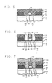
- an MOS IC which includes an n-channel MOSFET is fabricated by forming relatively thin GOXs 30 and a relatively thick FOX 40 on the surface of a layer of doped semiconductor material 20.
- the layer 20 constitutes the surface active layer of a substrate 10 of semiconductor material. If the MOS IC includes both n-channel and p-channel MOSFETs, then the substrate 10 will necessarily include both p-type and n-type bulk regions. In what follows, it is assumed the n-channel MOSFET is fabricated in a p-type bulk region having a doping level of, for example, 1016cm ⁇ 3.
- the relatively thick FOX 40 separates the GOX-covered GASAD (gate-and-source-and-drain) areas 50, on the surface of the layer 20, where MOSFETs are to be formed. If, for example, the active layer 20 is of silicon, then the GOXs 30 and the FOX 40 will typically be, respectively, relatively thin and thick layers of SiO2.
- the FOX 40 is formed, for example, by thermally oxidizing the surface of the layer 20. After opening windows in the FOX (by conventional techniques) to expose the GASAD areas 50 on the surface of the layer 20, the GOXs 30 are formed, for example, by again thermally oxidizing the surface of the layer 20.
- the thickness of the SiO2 GOXs 30 ranges from about 15nm (150 ⁇ ) to about 100nm (1000 ⁇ ) and is preferably about 20 nm (200 ⁇ ) Thicknesses of the GOXs 30 less than about 15nm (150 ⁇ ) are undesirable because such thin layers are likely to undergo dielectric breakdown. On the other hand, thicknesses greater than about 100nm (1000 ⁇ ) are undesirable because device operation requires the application of undesirably high voltages.
- the thickness of the SiO2 FOX 40 of the MOS IC ranges from about 200nm (2000 ⁇ ) to about 800nm (8000 ⁇ ) and is preferably about 400nm (4000 ⁇ )
- a thickness less than about 200nm (2000 ⁇ ) is undesirable because voltages applied to runners may invert underlying semiconductor material.
- a thickness greater than about 800nm (8000 ⁇ ) is undesirable because so thick a layer makes it difficult to subsequently achieve conformal deposition of metals, such as aluminum.
- a layer of gate material e.g. a layer of polysilicon
- the thickness of the deposited gate material, and thus the thickness of the gates ranges from about 200nm (2000 ⁇ ) to about 800nm (8000 ⁇ ,) and is preferably about 600nm (6000 ⁇ )
- Thicknesses less than about 200nm (2000 ⁇ ) are undesirable because such thin layers have undesirably high sheet resistance and may be excessively eroded during etching of the via holes through the interlevel dielectric.
- Thicknesses greater than about 800nm (8000 ⁇ ) are undesirable because it is difficult to achieve essentially vertical, gate sidewalls when etching such thick layers.
- dopants which are subsequently diffused into the active layer 20 to form the sources and drains of the MOSFETs
- the useful dopants include, for example, phosphorus, arsenic, and antimony.
- the incident energies of these dopants ranges from about 10 keV to about 300 keV, and is preferably about 100 keV. Energys less than about 10 keV are undesirable because the resulting junctions are undesirably shallow. Energys greater than about 300 keV are undesirable because the resulting junctions are undesirably deep, i.e., extend to a depth greater than 1 ⁇ m after diffusion.
- the substrate 10 will also include an n-type bulk region (in which the p-channel MOSFETs are formed) having a typical doping level of about 1016cm ⁇ 3.
- the useful p-type dopants to be implanted into the active layer of the n-type bulk region, e.g., n-type silicon, for subsequently forming the sources and drains of the p-channel MOSFETs include boron, aluminum, and gallium. The incident energies of these dopants is generally the same as that given above.
- the interlevel dielectric 70 is now deposited onto the FOX 40, the gates 60, as well as onto the implanted portions of the GASAD regions 50.
- the interlevel dielectric 70 includes, for example, SiO2-P2O5 or SiO2-P2O5-B2O3, materials which are readily deposited using conventional CVD techniques.
- the thickness of the interlevel dielectric 70 ranges from about 1/2 ⁇ m to about 2 ⁇ m, and is preferably about 1 ⁇ m. Thicknesses less than about 1/2 ⁇ m are undesirable because such thin layers are relatively poor insulators. Thicknesses greater than about 2 ⁇ m are undesirable because such thick layers result in relatively poor step coverage during subsequent metallization.
- the upper surface of the deposited interlevel dielectric 70 is typically nonplanar (which is generally undesirable during subsequent processing).
- the substrate is heated to temperatures ranging from about 850 degrees C to about 1100 degrees C, over corresponding time periods ranging from about 1 hour to about 2 hours. Temperatures less than about 850 degrees C, and heating times less than about 1 hour, are undesirable because they produce an undesirably small amount of glass flow. Further, temperatures greater than about 1100 degrees C, and heating times greater than about 2 hours, are undesirable because they produce undesirably deep junctions.
- the interlevel dielectric is patterned (using conventional techniques) to open via holes 100, 110, and 120 to, respectively, the sources, drains, and gates. If the electrical contacts (to be subsequently formed) to the sources, drains and gates are to include aluminum, and the substrate 10 is of silicon, then a barrier (130, 140 and 150) to the interdiffusion of aluminum and silicon is formed over each source and drain (and gate).
- the diffusion barrier includes, for example, a region of tungsten. Alternatively, this barrier includes a region of titanium, tantalum, molybdenum or rhenium.
- the thickness of the diffusion barrier ranges from about 30nm (300 ⁇ ) to about 150nm (1500 ⁇ ) and is peferably about 100nm (1000 ⁇ ) Thicknesses less than about 30nm (300 ⁇ ) are undesirable because such thin regions are relatively poor diffusion barriers. Thicknesses greater than 150nm (1500 ⁇ ) are undesirable because, for example, they lead to loss of selectivity in tungsten formation.
- the diffusion barriers 130 and 140 are of tungsten, then useful thicknesses of tungsten are readily selectively formed on the sources and drains by reactive WF6 and H2. Moreover, and to reduce the excessive etching of the n+ sources and drains, SiH4 is also introduced.
- the flow rate of the WF6 ranges from about 1 sccm to about 30 sccm, and is preferably about 10 sccm. A flow rate less than about 1 sccm is undesirable because it results in an undesirably low rate of tungsten formation. A flow rate greater than about 30 sccm is undesirable because it leads to excessive corrosion of the apparatus used in forming the tungsten.
- the flow rate of the H2 ranges from about 100 sccm to about 5000 sccm, and is preferably about 2000 sccm. Flow rates less than about 100 sccm are undesirable because they lead to excessive silicon erosion. Flow rates greater than about 5000 sccm are undesirable because they lead to undesirably high total pressures.
- the total pressure of the gases involved in the selective formation procedure ranges from about 13 Pa (100 millitorr) to about 260 Pa (2 Torr) and is preferably about 130 Pa (1 torr).
- the reaction temperature ranges from about 250 degrees C to about 600 degrees C, and is preferably about 300 degrees C or about 550 degrees C.
- Total pressures less than about 13 Pa (100 millitorr), and reaction temperatures less than about 250 degrees C, are undesirable because they result in relatively low tungsten formation rates.
- Total pressures greater than about 260 Pa (2 torr) are undesirable because they can lead to gas-phase nucleation of tungsten, rather than nucleation on the surfaces of the sources and drains.
- Reaction temperatures greater than about 600 degrees C are undesirable because they result in a loss of selectivity in tungsten formation.
- the appropriate concentration or concentration range of a silicon-containing gas, e.g. SiH4 is generally determined empirically by, for example, varying the concentration of SiH4 while monitoring both the rate of deposition of W (indicative of the reaction rate between WF6 and H2) and the etching (consumption) of source/drain silicon (via, for example, scanning electron micrographs of the sources and drains).
- the partial pressures of WF6, H2 and SiH4 corresponding to flow rates of 6 sccm, 4000 sccm and 40 sccm are, respectively, 0.396 Pa (2.97 x 10 ⁇ 3T), 264 Pa (1.98T) and 2.64 Pa (1.98 x 10 ⁇ 2T)).
- a layer of metal 160 e.g., an aluminum layer, is deposited onto the interlevel dielectric 70, as well as into the via holes leading to the sources, drains and gates.
- the thickness of the layer 160 ranges from about 1/2 ⁇ m to about 2 ⁇ m. Thicknesses less than about 1/2 ⁇ m are undesirable because they lead to undesirably high sheet resistance. Thicknesses greater than about 2 ⁇ m are undesirable because it is difficult to achieve essentially vertical sidewalls during the patterning of such thick layers.
- the metal layer 160 is patterned, e.g., selectively reactive ion etched, to form interconnecting metal runners which terminate in metal contact pads. The resulting substrate is then annealed at temperatures of, for example, 450 degrees C for about 1 hour to eliminate radiation damage incurred during the reactive ion etching.
- the MOS IC is finally completed by a series of conventional steps which typically includes the deposition of a silicon nitride layer, by the conventional technique of plasma-enhanced CVD, onto the IC to form a barrier against moisture and mechanical damage.
- the MOS IC is distinguishable from previous such ICs in that the formation of the diffusion barriers results in n+ sources and drains which are substantially free of erosion.
- a source or drain is substantially free of erosion, for purposes of the invention, provided the length of a perpendicular extending from a least-squares-fit planar approximation to the original substrate surface to the lowest point of the interface between the diffusion barrier and the source or drain is less than or equal to about 300 ⁇
- the metal contacts to all the sources and drains of the IC, including the source and drain of the n-channel MOSFET exhibit contact resistivities which are less than about 10 ⁇ 6ohm-cm2, and typically even less than about 5 x 10 ⁇ 7ohm-cm2.
- the contact resistivity to a source or drain is the multiple of the contact resistance, R c , to the source or drain and the area, A, of the upper surface of the source or drain.
- the former is readily determined by first measuring the current-voltage (I-V) curve across a region of the device substrate containing the source or drain.
- the area, A, of the upper surface, and the depth, d , of the source or drain are then measured using conventional techniques such as scanning electron microscopy, transmission electron microscopy, or secondary ion mass spectroscopy. Based upon the measured values of A and d , the ideal I-V curve for the source or drain is then calculated as taught, for example, in S.M. Sze, Physics of Semiconductor Devices , (John Wiley and Sons, N.Y), 2nd edition, p. 304. Typically, the measured I-V curve will be displaced from the theoretical I-V curve by a constant amount. Significantly, R c is related to this displacement, i.e.
- R c ⁇ V/I, where ⁇ V denotes the difference in the voltage values between the two I-V curves corresponding to a fixed current, I.
- R c is readily measured by applying an increasing, forward-biasing voltage across the source or drain, and measuring the corresponding values of dV/dI, the derivative of the applied voltage with respect to the resulting source/drain current.
- the contact resistance is equal to the value of dV/dI at saturation, i.e. when dV/dI stops changing with increasing forward-bias).
- the above MOS IC is preferably fabricated to include a region of metal silicide, i.e. cobalt silicide, titanium silicide, platinum silicide, tantalum silicide, or molybdenum silicide, on the sources and drains, prior to forming the diffusion barriers, as described above.
- the metal silicide regions are advantageous because they result in thermally stable contact resistivities to the sources and drains of the MOS IC, including the source and drain of the n-channel MOSFET, which are even lower than those described above, i.e. lower than about 10 ⁇ 6ohm-cm2, and even lower than about 10 ⁇ 7ohm-cm2.
- Useful thicknesses of the metal silicide range from about 30nm (300 ⁇ ) to about 100nm (1000 ⁇ ) Thicknesses less than about 30nm (300 ⁇ ) are undesirable because such thin layers are often incapable of preventing the overlying metal from penetrating to the substrate, resulting in increased contact resistivities. Thicknesses greater than about 100nm (1000 ⁇ ) are undesirable because such thick layers require the consumption of an undesirably large amount of substrate material during silicide formation.
- the metal silicide regions are formed by depositing, e.g. rf-sputtering, the corresponding pure metal into the via holes in the interlevel dielectric, and then sintering (thus reacting the metal with the silicon of the sources and drains) in an inert atmosphere of, for example, argo.
- Useful thicknesses of deposited metal range from about 15nm (150 ⁇ ) to about 50nm (500 ⁇ ) Thicknesses less than about 15nm (150 ⁇ ) and greater than about 50nm (500 ⁇ ) are undesirable because they yield metal silicide thicknesses which are outside the range, given above.
- Useful sintering temperatures, and corresponding sintering times range from about 300 degrees C and about 1 hour to about 1000 degrees C and about 1 hour. Sintering temperatures less than about 300 degrees C, and sintering times less than about 1 hour, are undesirable because they yield incomplete reactions between the metal and the silicon. Sintering temperatures greater than about 1000 degress C, and sintering times greater than about 1 hour, are undesirable because they lead to undesirable reactions between the metal in the metal silicide and both silicon and silicon dioxide.
- the metal silicide regions are generally porous, and thus permit reactive entities, such as WF6, to react with, and thus erode, the silicon of the sources and drains. Moreover, the WF6 tends to leach out, and react with, the silicon of the metal silicides. AS a consequence, the above-described inventive technique is essential to preventing the erosion of the metal silicides, and to achieving substantially erosion-free sources and drains.
- a diffusion barrier-and-metal silicide-covered source or drain is substantially free of erosion provided the length of a perpendicular extending from a particular imaginary plane to the lowest point of the interface between the metal silicide and the source or drain is less than or equal to about 30nm (300 ⁇ )
- the imaginary plane of interest is positioned below (within the substrate), and is parallel to, the least-squares-fit planar approximation to the original substrate surface.
- the length of a perpendicular extending between the two planes is equal to the thickness of the corresponding, uniform layer of silicon consumed in forming the metal silicide.
- This thickness is readily inferable from the amount of metal in the metal silicide, which is readily determined using, for example, conventional Rutherford Back-Scattering techniques. If the source of silicon used in forming the metal silicide is not the source or drain, then the imaginary plane is just the least-squares-fit planar approximation to the original substrate surface.)
Landscapes
- Engineering & Computer Science (AREA)
- General Physics & Mathematics (AREA)
- Physics & Mathematics (AREA)
- Condensed Matter Physics & Semiconductors (AREA)
- Manufacturing & Machinery (AREA)
- Computer Hardware Design (AREA)
- Microelectronics & Electronic Packaging (AREA)
- Power Engineering (AREA)
- General Chemical & Material Sciences (AREA)
- Chemical Kinetics & Catalysis (AREA)
- Chemical & Material Sciences (AREA)
- Electrodes Of Semiconductors (AREA)
- Chemical Vapour Deposition (AREA)
- Insulated Gate Type Field-Effect Transistor (AREA)
Applications Claiming Priority (2)
| Application Number | Priority Date | Filing Date | Title |
|---|---|---|---|
| US254999 | 1981-04-16 | ||
| US25499988A | 1988-10-07 | 1988-10-07 |
Publications (2)
| Publication Number | Publication Date |
|---|---|
| EP0363065A2 true EP0363065A2 (fr) | 1990-04-11 |
| EP0363065A3 EP0363065A3 (fr) | 1990-07-25 |
Family
ID=22966407
Family Applications (1)
| Application Number | Title | Priority Date | Filing Date |
|---|---|---|---|
| EP89309788A Withdrawn EP0363065A3 (fr) | 1988-10-07 | 1989-09-26 | Procédé de fabrication de dispositifs |
Country Status (4)
| Country | Link |
|---|---|
| EP (1) | EP0363065A3 (fr) |
| JP (1) | JPH02170425A (fr) |
| KR (1) | KR900007056A (fr) |
| ES (1) | ES2015776A6 (fr) |
Citations (3)
| Publication number | Priority date | Publication date | Assignee | Title |
|---|---|---|---|---|
| EP0157052A1 (fr) * | 1984-03-16 | 1985-10-09 | Genus, Inc. | Couche composite de tungstène et silicium à basse résistivité |
| EP0245934A2 (fr) * | 1986-05-15 | 1987-11-19 | Varian Associates, Inc. | Dépôt du silliciure métallique par LPCVD |
| EP0298155A2 (fr) * | 1987-07-10 | 1989-01-11 | Kabushiki Kaisha Toshiba | Procédé pour former une couche de métal réfractaire |
Family Cites Families (3)
| Publication number | Priority date | Publication date | Assignee | Title |
|---|---|---|---|---|
| JPS6057925A (ja) * | 1983-09-09 | 1985-04-03 | Matsushita Electronics Corp | シリコン上へのタングステン膜の形成方法 |
| JPS6156412A (ja) * | 1984-08-28 | 1986-03-22 | Fujitsu Ltd | 半導体装置の製造方法 |
| JPS6250468A (ja) * | 1985-08-30 | 1987-03-05 | Hitachi Ltd | 薄膜のプラズマ気相成長方法 |
-
1989
- 1989-08-17 ES ES8902881A patent/ES2015776A6/es not_active Expired - Lifetime
- 1989-09-26 EP EP89309788A patent/EP0363065A3/fr not_active Withdrawn
- 1989-10-05 KR KR1019890014309A patent/KR900007056A/ko not_active Application Discontinuation
- 1989-10-06 JP JP1260336A patent/JPH02170425A/ja active Pending
Patent Citations (3)
| Publication number | Priority date | Publication date | Assignee | Title |
|---|---|---|---|---|
| EP0157052A1 (fr) * | 1984-03-16 | 1985-10-09 | Genus, Inc. | Couche composite de tungstène et silicium à basse résistivité |
| EP0245934A2 (fr) * | 1986-05-15 | 1987-11-19 | Varian Associates, Inc. | Dépôt du silliciure métallique par LPCVD |
| EP0298155A2 (fr) * | 1987-07-10 | 1989-01-11 | Kabushiki Kaisha Toshiba | Procédé pour former une couche de métal réfractaire |
Also Published As
| Publication number | Publication date |
|---|---|
| KR900007056A (ko) | 1990-05-09 |
| EP0363065A3 (fr) | 1990-07-25 |
| JPH02170425A (ja) | 1990-07-02 |
| ES2015776A6 (es) | 1990-09-01 |
Similar Documents
| Publication | Publication Date | Title |
|---|---|---|
| EP0377137B1 (fr) | Procédé de dépÔt sélectif de métal réfractaire sur des substrats de silicium | |
| CA1204045A (fr) | Metallisation au siliciure de cobalt pour transistors semiconducteurs | |
| US6770571B2 (en) | Barrier in gate stack for improved gate dielectric integrity | |
| US5336903A (en) | Selective deposition of doped silicon-germanium alloy on semiconductor substrate, and resulting structures | |
| US6903462B2 (en) | Chemical vapor deposition of titanium | |
| US4818723A (en) | Silicide contact plug formation technique | |
| US4540607A (en) | Selective LPCVD tungsten deposition by the silicon reduction method | |
| US6458699B1 (en) | Methods of forming a contact to a substrate | |
| US20060019475A1 (en) | Method of depositing polysilicon | |
| EP0126424A2 (fr) | Procédé pour la fabrication des structures en polyciures | |
| US5545574A (en) | Process for forming a semiconductor device having a metal-semiconductor compound | |
| US4398341A (en) | Method of fabricating a highly conductive structure | |
| US5801444A (en) | Multilevel electronic structures containing copper layer and copper-semiconductor layers | |
| EP0328970B1 (fr) | Procédé déposition de tungstène sur silicium dans un procédé CVD non auto-limitateur et dispositif à semiconducteur ainsi fabriqué | |
| US5071788A (en) | Method for depositing tungsten on silicon in a non-self-limiting CVD process and semiconductor device manufactured thereby | |
| US4968644A (en) | Method for fabricating devices and devices formed thereby | |
| EP0147913B1 (fr) | Procédé pour la fabrication d'un dispositif semi-conducteur comportant une technique de croissance en vapeur sélective | |
| US4587710A (en) | Method of fabricating a Schottky barrier field effect transistor | |
| US5202287A (en) | Method for a two step selective deposition of refractory metals utilizing SiH4 reduction and H2 reduction | |
| US5212400A (en) | Method of depositing tungsten on silicon in a non-self-limiting CVD process and semiconductor device manufactured thereby | |
| EP0472804A2 (fr) | Composés cuivre-semiconducteur pouvant être produits à température ambiante | |
| EP0460918A2 (fr) | Dispositif semi-conducteur avec transistor de type grille isolée amélioré | |
| JPH056866A (ja) | 半導体装置の製造方法 | |
| EP0363065A2 (fr) | Procédé de fabrication de dispositifs | |
| US5329161A (en) | Molybdenum boride barrier layers between aluminum and silicon at contact points in semiconductor devices |
Legal Events
| Date | Code | Title | Description |
|---|---|---|---|
| PUAI | Public reference made under article 153(3) epc to a published international application that has entered the european phase |
Free format text: ORIGINAL CODE: 0009012 |
|
| AK | Designated contracting states |
Kind code of ref document: A2 Designated state(s): BE DE FR GB IT NL |
|
| PUAL | Search report despatched |
Free format text: ORIGINAL CODE: 0009013 |
|
| AK | Designated contracting states |
Kind code of ref document: A3 Designated state(s): BE DE FR GB IT NL |
|
| 17P | Request for examination filed |
Effective date: 19901206 |
|
| 17Q | First examination report despatched |
Effective date: 19930430 |
|
| STAA | Information on the status of an ep patent application or granted ep patent |
Free format text: STATUS: THE APPLICATION IS DEEMED TO BE WITHDRAWN |
|
| 18D | Application deemed to be withdrawn |
Effective date: 19930911 |