EP0362901A2 - Milieu optique pour l'enregistrement de données numériques - Google Patents
Milieu optique pour l'enregistrement de données numériques Download PDFInfo
- Publication number
- EP0362901A2 EP0362901A2 EP89120942A EP89120942A EP0362901A2 EP 0362901 A2 EP0362901 A2 EP 0362901A2 EP 89120942 A EP89120942 A EP 89120942A EP 89120942 A EP89120942 A EP 89120942A EP 0362901 A2 EP0362901 A2 EP 0362901A2
- Authority
- EP
- European Patent Office
- Prior art keywords
- absorber
- medium
- accordance
- island
- film
- Prior art date
- Legal status (The legal status is an assumption and is not a legal conclusion. Google has not performed a legal analysis and makes no representation as to the accuracy of the status listed.)
- Withdrawn
Links
Images


Classifications
-
- G—PHYSICS
- G11—INFORMATION STORAGE
- G11B—INFORMATION STORAGE BASED ON RELATIVE MOVEMENT BETWEEN RECORD CARRIER AND TRANSDUCER
- G11B7/00—Recording or reproducing by optical means, e.g. recording using a thermal beam of optical radiation by modifying optical properties or the physical structure, reproducing using an optical beam at lower power by sensing optical properties; Record carriers therefor
- G11B7/004—Recording, reproducing or erasing methods; Read, write or erase circuits therefor
- G11B7/0045—Recording
-
- G—PHYSICS
- G11—INFORMATION STORAGE
- G11B—INFORMATION STORAGE BASED ON RELATIVE MOVEMENT BETWEEN RECORD CARRIER AND TRANSDUCER
- G11B7/00—Recording or reproducing by optical means, e.g. recording using a thermal beam of optical radiation by modifying optical properties or the physical structure, reproducing using an optical beam at lower power by sensing optical properties; Record carriers therefor
- G11B7/24—Record carriers characterised by shape, structure or physical properties, or by the selection of the material
Definitions
- This disclosure relates to optical media, to methods of preparing such media, and to associated techniques and apparatus which are adapted to detect a prescribed level of heat or prescribed radiation energy, especially with low power laser equipment.
- the invention consists in an optical medium for use in an optical heat detection system providing a focused monitor-beam of radiation of a pre-determined wavelength on said medium, said medium comprising at least one layer of absorber material deposited in discontinuous island form so as to be agglomerated upon application of a test level of heat energy whereby to detectably alter an optical characteristic so as to facilitate readout of the beam by associated optical detection means, the island-layers so formed presenting well-segmented islands of absorber material having an average width considerably smaller than the width of said beam.
- the invention consists in a method of preparing an improved radiation-sensing record blank wherein an information layer is disposed on substrate means and is adapted to respond to, and sense, a prescribed test level of energy while being monitored by a laser beam of prescribed energy and wavelength, this method including the steps of: depositing an absorber material to a pre-determined relatively miniscule depth on the substrate means such as to constitute a discontinuous record-film exhibiting an array of separated islands and having a virginal-reflectance so as to appear optically-continuous to said laser beam; whereby if such a test level of energy is received it will induce a prescribed agglomeration of the absorber islands to make the film appear more discontinuous optically and optically-apertured there, and to thereby shift the detected reflectance of the blank; the absorber material being selected and so vapor-deposited, in conjunction with the surrounding optical/thermal environment, as to so agglomerate.
- the invention consists in a system adapted to detect a test-level of energy, said system comprising source means for providing monitor radiation of a pre-determined wavelength, means for directing said radiation as a beam along a detect axis to present a predetermined energy level at an optical medium and associated detect means disposed along said axis with the medium interposed in beam intersecting relation with said source means; the medium comprising at least one ultra-thin, discontinuous layer of absorber material deposited in island form so as to be agglomerated upon application of said beam at said test level of energy whereby to alter an optical characteristic thereof for detection by said detect means; said island-film presenting well separated islands of the absorber material having an average width very considerably smaller than the width of said monitor beam.
- base AR comprises a "reflector" layer 3, on which a transmissive "spacer” layer 4 is laid.
- Layers 3 and 4 may be characterized as, respectively, primarily-reflective and primarily transmissive at the contemplated read/write wavelengths.
- Layers 3, 4, 5 will be understood as providing a multi-layer, low- reflecting (anti-reflection) design over most of the visible spectrum as known in the art (see Ash article).
- Support 2 preferably comprises a polished aluminum disk of the type presently used in digital magnetic recording for computer disk drives, coated with an organic smoothing (subbing) layer 2-S adapted to render a satisfactorily-smooth, flat surface for deposition of reflector layer 3.
- an organic smoothing (subbing) layer 2-S adapted to render a satisfactorily-smooth, flat surface for deposition of reflector layer 3.
- a radiation (laser) beam of prescribed energy and wavelength may be understood as applied to medium 1 from a laser source L, so as to establish a "pit” or like "deformation” on layer 5 as “writing” takes place (e.g., at site “v” shown in phantom). More particularly, it will be desired to use a 10 mW gaussian beam with diameter of 0.8 ⁇ m (i.e., 800 nm or 1/E) and scanning at 45 m/sec., to form a "pit” with a certain minimum length and width of 0.8 ⁇ m (though not necessarily circular or other prescribed shape, -this requirement is too stringent for conventional means however).
- surface reflectance on absorber 5 can be made “zero” or a selected value by adjusting absorber thickness and spacer thickness.
- a "tri-layer” being here understood as comprising a transparent spacer with absorber on one face and reflector on the other).
- the reflector film may be eliminated (e.g., in favor of a "dielectric mirror") and that spacer 4 may comprise other materials/structures (e.g., several layers of like material that is also more insulative thermally).
- the coating parameters here will be understood as selected to preferably provide an "anti-reflective" condition for the so-coated disk at the contemplated recording frequency when the write beam is focused on this absorber layer.
- Anti-Reflection Structures for Optical Recording by Bell and Spong, Journal of Quantum Electronics, Vol. QE 14, No. 7, July, 1978; and for general prior art, see exemplary articles: “Optical Disk Systems Emerge”, IEEE Spectrum by Bartolini, et al, August 1978, page 20; and “Optical Recording Media Review” by Bartolini, SPIE Proceedings, Vol. 123, 1977, page 2; “Optical Storage Materials and Methods", SPIE Proceedings, Vol. 177, Optical Information Storage, 1979, page 56].
- deposition proceeds by thermal evaporation until the reflectance of layer 5 reaches a predetermined reflectance level.
- this may be done empirically, or by continually monitoring the reflectance of the absorber film (e.g., on a witness-chip) as layer 5 is deposited (see deposition techniques described by Zech in his cited article) or by like suitable optical techniques for deposition-monitoring; or by other known methods, such as monitoring deposited mass or by electrical properties.
- the reflectivity of the record medium 1 will be understood as modified at each bit-site “v” by the radiation beam from write-laser L, so that, upon detection with a suitable means, the "void areas” v (i.e., "pits") may be distinguished as relatively “high reflectance spots” from the low reflectance "non-void” background surrounding them, as known in the art:
- Tellurium is a "low melting point/poor conductivity" metal commonly preferred by workers because it is felt to exhibit superior sensitivity, thus minimizing required (threshold) laser write-power.
- Absorber layer 5 preferably comprises a relatively thin layer of tellurium which is vapor deposited (thermally evaporated) onto spacer layer 4 (on a relatively flat -- ⁇ 1/20 ⁇ -- record surface thereof.
- the Te is so evaporated in a high vacuum preferably using a large batch coating chamber with corresponding large coating distances and "double-rotation" of substrate, etc. to better ensure uniformity -- e.g., using a refractory metal boat for a source [1.2 m box type coating chamber used in Ash article]. All dust and stains on parts should be reduced to a strict minimum, using the most rigorous "Clean Room” techniques.
- Substrate 2 comprises a flat, aluminum plate polished to desirable flatness and coated with "subbing" 2-S to appropriate flatness to accommodate deposition of thin reflector layer 3 (high reflectivity over at least the "working portion" of the contemplated radiation spectrum).
- "subbing" 2-S to appropriate flatness to accommodate deposition of thin reflector layer 3 (high reflectivity over at least the "working portion" of the contemplated radiation spectrum).
- About 60 -90 nm of aluminum prefer about 60 nm, vapor-deposited
- aluminum is not a perfect reflector, workers will recognize that in some cases one will substitute a "multi-layer dielectric stack" or the like.
- Spacer 4 is likewise deposited atop reflector 3.
- Spacer 4 is a dielectric material which is relatively transparent to the "working portion" of the laser spectrum.
- the tellurium absorber layer 5 will be understood as highly absorptive of the contemplated recording laser spectrum (e.g., typically 25% absorptive; 30% reflective; with about 45% of the beam energy transmitted (for tri-layer cancellation, must transmit more than reflect).
- the thickness of absorptive layer 5 depends on that of spacer 4. Where transmitted light should be reduced, one may wish to increase spacer thickness (in N x X/4 periods -- also reducing heat-loss possibly).
- Te absorber 5 with its low melting point and a relatively short thermal diffusion length (poor conductivity) as a good, "high sensitivity” material which helps conserve incident laser energy.
- a write beam from laser source L falls upon site “v" of layer 5, a small portion of its energy will be reflected, a small portion absorbed and a large portion transmitted -- the transmitted portion being reflected back by layer 3 to be (principally) absorbed in layer 5.
- both incident and reflected energy will heat film 5, minimizing transmission losses (note: deposition of 5 yielded a "tri-layer”).
- Variations in absorber thickness or uniformity should be scrupulously avoided since this can reduce the write-energy coupled into the absorbing film and degrade sensitivity.
- Sensitivity will be understood as characterizing the write-energy E w necessary to change reflectivity (or a like read-out characteristic) sufficient to give the specified minimum read-out.
- the intensity and time exposure of the focused Write-Beam will be understood as sufficient to so elevate the temperature of absorber layer 5 as to cause the indicated change in reflectivity (at v sites) giving the desired read-out quality, etc. (e.g., so that adequate contrast, S/N ratio) may be realized, as understood by workers in the art, -- cf. an exemplary S/N ratio of 40-50 dB (peak-to-peak signal vs. RMS noise) for a bandwidth of about 15 MHz.
- Such a spot may be read-out with means known in the art; e.g., with a similar laser at low power (e.g., above described laser at 3 mW), the increase in reflected energy received (at a suitable photo-detector) is observed to yield an output signal representing the recorded bits, these being readily distinguishable from background this read-energy being insufficient to "erase” or disturb the so-recorded bits, of course.
- a frequency f R where "pit-depth" introduces a phase change vs. light reflected at surface of Te such as to maximize contrast therewith].
- Te film of Example I will be found characterized by a rapid increase in overall optical transmission after such "aging”. This is presumably caused by a general oxidation of the metal as well as severe selected site-attack beginning at "defect sites” in the metal film, (of. analogous test per MIL SPEC #810-B).
- FIG. 2 shows an example I; absorber of gold material
- Record 10 will be understood as comprising a support 12 on which an "anti-reflective" base 1-AR is laid (like AR in FIG. 1, preferably comprising a reflective layer 13, with a transmissive spacer layer 14 laid upon 13), with absorber film 15 placed atop substrate 1-AR (spacer 14 thereof).
- absorber 15 comprises a film of "gold material” comprising an “island layer” deposited to function as an absorber film (somewhat like the Te film in the "Te Example", e.g. in a somewhat similar process and by similar means).
- absorber thickness is controlled so that it yields a prescribed minimal "Dark Mirror” reflectance R m (e.g., here 10% was chosen) as further described below.
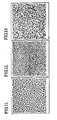
- film 15 is formed to be discontinuous, being formed in an island configuration for optimal results, as shown in FIG. 11 (100,000 x Te micrograph) and as described below.
- the underlying spacer layer 14, reflector layer 13 and substrate 12 are (at least functionally) otherwise the same as in “Te Example”, and thus will be understood as functioning as a “tri-layer”, with absorber 15, as understood in the art (e.g., see cited references).
- gold absorber film 15 is preferably formed by vapor depositing a gold material on the surface of Si0 2 spacer 4 until (monitoring the well known "tri-layer” effect) surface-reflectivity of 5 first drops to preselected value R m (10% reflectance here), taking care to render the "insular" configuration.
- Reflectance R m may, conveniently, be set at any desired value consistant with adequate “writing” and read-out. Here, about 10% was arbitrarily selected (minimum for proper focusing, etc.
- Absorber layer 15 thus comprises an extremely thin "island-deposit" of gold which is vapor-deposited (thermally evaporated) onto spacer layer 14 (i.e., on a relatively flat; e.g., 0.5 X record-surface thereof).
- spacer layer 14 i.e., on a relatively flat; e.g., 0.5 X record-surface thereof.
- the absorber film 15 is thus preferably vacuum deposited on spacer layer 14 using present preferred techniques (e.g., "pure” gold has been so deposited in large vacuum chamber at - 10- 6 - 10-7 Torr. (1.333 x 10- 4. -1.333 x 10- 5 Pa), from a molybdenum boat which was resistance-heated -- deposition rate was about 0.5-1 nm/sec.).
- present preferred techniques e.g., "pure” gold has been so deposited in large vacuum chamber at - 10- 6 - 10-7 Torr. (1.333 x 10- 4. -1.333 x 10- 5 Pa), from a molybdenum boat which was resistance-heated -- deposition rate was about 0.5-1 nm/sec.
- the silica layer 14 was, itself, likewise vapor-deposited before receiving the gold film 15. All substrates were cleaned according to present good practice for optical thin films.
- this may be done empirically, or by continually monitoring the surface-reflectance of a witness-chip while absorber film 15 is deposited until satisfactory "islands" appear (and see deposition techniques described by Zech in his cited article, or by other known methods, such as monitoring deposited mass or electrical properties during deposition).
- bit sites appear to be "agglomerate-holes" (where absorber has been made to “agglomerate” and where absorber material may also be caused to migrate toward the hole-periphery, or beyond) -- this across a hole-diameter comparable to that of the read-beam (e.g., 1 ⁇ 4- 3/4 thereof); to exhibit a like increase in reflectance and higher output signal.
- FIG. 6 is an artistic rendering showing such an "agglomerate-hole” (or “quasi-pit") as seen in photomicrographs of such records.
- an "agglomerate-hole” 15p will be understood as a somewhat- circular written-spot, or physical-optical discontinuity in the virgin unwritten absorber film 15 " .
- Spot 15p will be on the order of laser beam-diameter (e.g., 40-120% thereof) and may include a "rim" or partial-rim about its periphery, Within the rim, relatively less absorber material is usually present; what there is will be seen as consolidated into absorber-globs gL, most of which are relatively large (e.g., usually fewer, many being larger than the tiny "islands” of virgin film 15 v and FIG. 11, (and lie relatively farther apart). In effect, spots 15 P will be understood as constituting an "optical void” or discontinuity at the selected read-wavelength ( ⁇ w); whereas the virgin island film 15 v appears as a relatively continuous (partial) reflector.
- FIG. 11 is'a microscopic plan view (100,000 x TE micrograph) of the original,virgin (i.e., unrecorded- upon) reflecting surface of an Au absorber film like that above-described. It will be evident that this surface appears as a physically discontinuous, or partly discontinuous, "insular" configuration, exhibiting a fairly regular pattern (semi-islands on the Si0 2 spacer). For this Ex. I, the islands will be understood as having diameters on the order of a few tens nm (e.g., 10-30 nm typical), separated by intervals of comparable dimension (e.g., 5-20 nm apart -- vs. laser beam 500-1,000 nm wide; of 632.8 nm wavelength). The virgin film 15 will thus exhibit a certain "% void" range (e.g., a few to 10% voids).
- At least some of the first-order factors controlling such island formation are: absorber material, deposition-rate, adhesion; substrate material and. condition (e.g., cleaning, roughness, etc.) and temperature; presence of "nucleation layer", presence of vapor-contaminants (vacuum pressure) and like factors as will be appreciated by workers. For example, too-cool a substrate will render a continuous film, but too-hot will leave no film at all.
- workers may compare FIGS. 12 and 13 with referenced FIG. 11.
- a similar film was prepared (like Ex. I) except that the silica substrate was coated with a bismuth oxide layer for nucleation as known in the art.
- FIG. 13 was similar, with a chromium nucleation layer instead. Compared with FIG, 11, FIG. 12 seemed to exhibit thinner islands farther apart, while FIG. 13 is a continuous gold film (no islands).
- the cited laser apparatus could not "write” at all on the film of FIG. 13 (at cited power level); while the film of FIG. 12 wrote like that of FIG. 11 (Ex. I) except for a bit lower sensitivity.
- the write-beam is assumed, here, to so affect the islands in a bit-site as to cause "agglomeration" and the (usually) attendant increase in average island size and spacing (increased % void area).
- the initial (virgin) % void will be sufficient to accommodate a prescribed minimal heat loss, radially, yet not so large that initial reflectance (R o ) exceeds the desired "near zero" value (required for a "Dark Mirror").
- this writing operation may describe this writing operation as so energizing the absorber film as to, in effect, significantly separate absorber mass at the bit site.
- a "so-written" spot may shift these values to about 30% - 10% - 60%, respectively, for the subject write wavelength (tri-layer).
- the island configuration of the film may account for this apparently-reduced melting point, or it may trigger a write mechanism other than "gross melting" -- one is not yet sure.
- One theory is that such islands possess such high internal energy that relatively little write beam-energy can trigger their "bursting” and so agglomerating, yet without necessarily “melting them as such”.
- Te Example was also run with a thin overcoating of SiO (10 nm, vapor deposited) on the Te absorber film.
- this SiO coat did affect "pit formation", raising required write-energy to about double. (Possibly because it so "squeezed” the Te film at the pit-site as to impede associated displacement of Te material there).
- insular absorber films can be used to make OD disks as contemplated (e.g., satisfying all or most of the requirements of Table I).
- the (evaporo-deposited) absorber constitutes gold plus a minor concentration of tin. This is laid-down as a laminate for convenience of deposition: first gold, then tin, then gold (alternatively, one can add other dual layers of tin and gold too). Upon heating, this "laminate" should inter-diffuse to form (mostly) a Au/Sn alloy (mostly gold, so "gold characteristics" should predominate).
- This Au/Sn film is substituted as the island-film of Ex. I (for 15 in FIG. 2) and is similarly written-upon. Effects: were qualitatively similar to Ex. I, while exhibiting greatly superior archivabiiity and somewhat inferior sensitivity.
- FIG. 5 depicts a replication of Ex. I, (FIG. 2), except that a clear polymer is used as spacer (e.g., Teflon) and a tin-flash ("strike", as adhesion promotor, etc.) is interposed under the pure-gold absorber.
- spacer e.g., Teflon
- tin-flash e.g., adhesion promotor, etc.
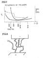
- FIG. 7 a plot of wavelength vs. reflectance (and index of refraction) of virginal island films.
- a pure gold island absorber like that of Ex. I might exhibit a shift in refractive index as portrayed by curve A and a reflectance/x characteristic as in curve B. This obviously inhibits operating well above or below the Ne-Ne laser spectrum (633.8 nm-- e.g., desired formatting of OD disks is not feasible at 440 nm, etc.; alternate use of Ga-As laser not feasible either).
- adding the Sn (island-) strike served to "flatten" the absorber's reflectivity curve as indicated at curve C. Workers will appreciatehow significant such an increased radiation bandwidth can be.
- the polymer is quite heat-degradable; accordingly the deposition steps (for Sn, then Au) will keep within its temperature limits (- 100 ⁇ C)
- Such gold films should be equal to the "archival” conditions specified here. It is projected that such "gold records” can maintain adequate read-out (30 + dB) for the order of ten (10) years under typical contemplated storage and use conditions.
- Ex. III is replicated except that a thin layer of Si0 2 is superposed on the polymer spacer 214 (FIG. 5), with the Sn strike deposited on the Si0 2 then the gold.
- FIG. 4 is an idealized showing of a typical "agglomerate-hole" written on such an Au/Sb absorber, the "virgin" island configuration v not shown here.
- Ex. III is replicated (Sn strike on polymer), except that an antimony "strike” follows the Sn strike, with gold deposited thereafter.
- the absorber film 15 (FIG. 2) comprises successive island-layers of: gold-lead-gold-lead-gold, each in proper island configuration. When heated, these island layers will readily inter-diffuse (distances so short) to form Au/Pb alloy-islands (Au major constituent, so ignore Pb properties as a first approximation, i.e. thus alloy will exhibit "gold characteristics" predominantly).
- film 15 is so deposited as a "laminate" for testing convenience, other methods will occur to workers.
- these filamentary peninsulae exhibit a much lower electrical resistance laterally (still quite high though) than the "islands" of Ex. I, etc. -- yet since they function similarly to write an "agglomerate-hole" it is assumed they retain much of the "thermal isolation" of the aforementioned "islands".
- such a filamentary configuration may also be characterized as “insular”. It records like the other "insular” films forming "agglomerate holes”.
- Sensitivity here was maximal; better than with pure gold (Ex. I) -- e.g., approximately as “sensitive” as a tellurium absorber; often better, (e.g., about the sensitivity of "Te Example” has been measured). That is, information can be satisfactorily “written” on the gold-lead tri-layer here in the power regime of 5-15 mW/10-100 n.sec. (or 100-1000 p.J.). More specifically, about 5 mW for as little as 40 n.sec. is seen to "switch reflectivity". Some samples even "switch" in about 10-15 n.sec.
- one general teaching hereof is that, in fashioning OD disks with an absorber film in "tri-layer configuration" as described, one can achieve surprisingly good sensitivity by laying-down the absorber material in island form.
- chat noble metals like gold, palladium, etc. or their alloys may be so deposited as the absorber -- e.g., to enhance archival life while securing good sensitivity.
- an island-film absorber like gold can be combined with a co-constituent like lead or antimony (e.g., in a minor %) to enhance sensitivity, and/or with a co-constituent like tin to enhance archivability and optical characteristics (e.g., increased bandwidth).
- a co-constituent e.g., Au plus Pb or Pd plus Sn minimizes likelihood of "ejecta"; Au plus Sn and Sb to enhance S y, A y, bandpass and reduce ejecta.
- FIG. 9 shows
- FIG. 9 schematically illustrates another application of the subject "radiation-agglomerated" island-films.
- an island-film (ab.) is understood as deposited on a suitable substrate (e.g., Au or Au alloy on glass, with clear polymer overcoat, similar to above Examples) within a frame member f.
- a radiant energy source LS e.g., He-Ne laser at 633.8 nm suitable mW
- LS is understood as constantly (or periodically) directing an incident beam b i onto film ab.
- film ab is adapted to reflect most of beam b i (e.g., as reflect beam b, toward a first detect unit Di).
- LS e.g., to agglomerate-temperature -- such as by a fire, flames nearby, etc.
- film ab now looks relatively transparent to ⁇ i .
- ab will pass beam b i , as transmitted beam b t apt for detection at an associated second detect unit D 2 .
- source LS could be normally inactive, but upon first emitting energy, direct a portion (as beam b;) to unit D 2 and thereby melt an aperture in film ab.
- beam b i could be scanned once across film ab to "write” .a pattern therein -whereupon, with b; inactivated, a source of "backlighting illumination” could be projected at the entire "mask” so-etched (e.g., to generate a display or an optical printing plate). Workers will contemplate other like applications.
- Such"island"(or “insular”) films may comprise other metals or their alloys in certain cases (e.g., other binary alloys of Au or Pd, ternary alloys, etc. or other metals such as P t , Cu, Ag, R h ).
- the absorber film will be advantageously combined in an anti-reflection or like optical background array.
- Such island films may, in certain instances, be otherwise deposited, e.g., by other vapor-deposition techniques (vapor-deposition is very practical where, as in Ex. I, etc., it may also be used to deposit other related layers such as the reflector, spacer, etc.). Vapor co-deposition will usually be preferred for "alloys". Other methods may be feasible for depositing the absorber, such as sputtering. In any event, it will usually be preferred to monitor the film during deposition to closely control the deposited island configuration.
Landscapes
- Thermal Transfer Or Thermal Recording In General (AREA)
Priority Applications (1)
| Application Number | Priority Date | Filing Date | Title |
|---|---|---|---|
| EP19890120942 EP0362901A3 (en) | 1982-05-25 | 1983-05-24 | Heat sensitive film shutter |
Applications Claiming Priority (3)
| Application Number | Priority Date | Filing Date | Title |
|---|---|---|---|
| US38168782A | 1982-05-25 | 1982-05-25 | |
| US381687 | 1982-05-25 | ||
| EP19890120942 EP0362901A3 (en) | 1982-05-25 | 1983-05-24 | Heat sensitive film shutter |
Related Parent Applications (2)
| Application Number | Title | Priority Date | Filing Date |
|---|---|---|---|
| EP83302972A Division EP0096503A3 (fr) | 1982-05-25 | 1983-05-24 | Obturateur en couche mince sensible à la chaleur |
| EP83302972A Division-Into EP0096503A3 (fr) | 1982-05-25 | 1983-05-24 | Obturateur en couche mince sensible à la chaleur |
Publications (2)
| Publication Number | Publication Date |
|---|---|
| EP0362901A2 true EP0362901A2 (fr) | 1990-04-11 |
| EP0362901A3 EP0362901A3 (en) | 1990-10-24 |
Family
ID=26120750
Family Applications (1)
| Application Number | Title | Priority Date | Filing Date |
|---|---|---|---|
| EP19890120942 Withdrawn EP0362901A3 (en) | 1982-05-25 | 1983-05-24 | Heat sensitive film shutter |
Country Status (1)
| Country | Link |
|---|---|
| EP (1) | EP0362901A3 (fr) |
Cited By (1)
| Publication number | Priority date | Publication date | Assignee | Title |
|---|---|---|---|---|
| WO1991020078A1 (fr) * | 1990-06-19 | 1991-12-26 | Basf Aktiengesellschaft | Procede de stockage optique de donnees |
-
1983
- 1983-05-24 EP EP19890120942 patent/EP0362901A3/en not_active Withdrawn
Non-Patent Citations (1)
| Title |
|---|
| IBM TECHNICAL DISCLOSURE BULLETIN. vol. 25, no. 8, January 1983, NEW YORK US pages 4200 - 4202; K.Y.AHN and S.R.HERD: "Long-life gold based optical storage materials" * |
Cited By (1)
| Publication number | Priority date | Publication date | Assignee | Title |
|---|---|---|---|---|
| WO1991020078A1 (fr) * | 1990-06-19 | 1991-12-26 | Basf Aktiengesellschaft | Procede de stockage optique de donnees |
Also Published As
| Publication number | Publication date |
|---|---|
| EP0362901A3 (en) | 1990-10-24 |
Similar Documents
| Publication | Publication Date | Title |
|---|---|---|
| US4430659A (en) | Protuberant optical recording medium | |
| US4470053A (en) | Protuberant optical recording medium | |
| EP0079231B1 (fr) | Procédé optique pour l'emmagasinage de données numériques d'archives | |
| EP0096504B1 (fr) | Feuilles d'enregistrement aureuses, destinées à des fins archivistiques, pour mettre en mémoire des données digitales | |
| EP0098046B1 (fr) | Feuilles d'enregistrement destinées à des fins archivistiques pour mettre en mémoire des données digitales en utilisant un laser à écrire à puissance basse | |
| EP0098045B1 (fr) | Feuilles d'enregistrement contenant de l'or, destinées à des fins archivistiques, pour mettre en mémoire des données digitales en utilisant un laser à écrire à puissance basse | |
| EP0362901A2 (fr) | Milieu optique pour l'enregistrement de données numériques | |
| EP0096503A2 (fr) | Obturateur en couche mince sensible à la chaleur | |
| EP0096501B1 (fr) | Procédé de détection d'incendie | |
| EP0097430A1 (fr) | Procédé de détection d'incendie | |
| EP0096502A1 (fr) | Feuilles d'enregistrement isolées, insulaires, pour mettre en mémoire des données digitales en utilisant un laser à écrire à puissance basse | |
| EP0079741B1 (fr) | Moyens d'enregistrement d'archives à couche d'informations améliorée et substrat y associé | |
| US5177732A (en) | Optical recording using an agglomerating recording medium which changes reflectivity upon recording | |
| EP0079229B1 (fr) | Dispositif d'emmagasinage de données numériques sur un moyen d'enregistrement optique d'archives à l'aide de rayonnement à faible énergie | |
| EP0139507B1 (fr) | Feuilles d'enregistrement insulaires et leur fabrication | |
| EP0079230A2 (fr) | Préparation de moyens d'enregistrement d'archives pour l'emmagasinage de données numériques | |
| EP0079232A2 (fr) | Système d'enregistrement de données d'archives à l'aide de rayonnement à faible énergie et moyens y associés | |
| TWI478160B (zh) | 包含碳層及金屬層之資料儲存媒體及製備光學資訊媒體之方法 | |
| WO1983001703A1 (fr) | Procede d'enregistrement de donnees d'archivage et supports s'y rapportant | |
| JPS59500438A (ja) | 低出力書込レ−ザを用いるディジタル・デ−タ・ストレ−ジに適した金記録保存フィルム | |
| JPS59500439A (ja) | 低出力書込レ−ザを用いるディジタル・デ−タ・ストレ−ジに適した記録保存フィルム | |
| JPS59500886A (ja) | ディジタル・デ−タ・ストレ−ジに適した第1金の記録保存フィルム | |
| JPS59500991A (ja) | ディジタル・デ−タ・ストレ−ジに適したアイランド状の記録フィルム | |
| JPS59500883A (ja) | 低出力書込レ−ザを用いるディジタル・デ−タ・ストレ−ジに適した金合金記録保存フィルム | |
| JPS59500992A (ja) | 低出力書込レ−ザを用いるディジタル・デ−タ・ストレ−ジに適したアイランド状熱絶緑性記録フイルム |
Legal Events
| Date | Code | Title | Description |
|---|---|---|---|
| PUAI | Public reference made under article 153(3) epc to a published international application that has entered the european phase |
Free format text: ORIGINAL CODE: 0009012 |
|
| 17P | Request for examination filed |
Effective date: 19891111 |
|
| AC | Divisional application: reference to earlier application |
Ref document number: 96503 Country of ref document: EP |
|
| AK | Designated contracting states |
Kind code of ref document: A2 Designated state(s): BE DE FR GB NL SE |
|
| PUAL | Search report despatched |
Free format text: ORIGINAL CODE: 0009013 |
|
| AK | Designated contracting states |
Kind code of ref document: A3 Designated state(s): BE DE FR GB NL SE |
|
| STAA | Information on the status of an ep patent application or granted ep patent |
Free format text: STATUS: THE APPLICATION IS DEEMED TO BE WITHDRAWN |
|
| 18D | Application deemed to be withdrawn |
Effective date: 19910425 |