EP0362079B1 - Microstrip antenna - Google Patents
Microstrip antenna Download PDFInfo
- Publication number
- EP0362079B1 EP0362079B1 EP89402694A EP89402694A EP0362079B1 EP 0362079 B1 EP0362079 B1 EP 0362079B1 EP 89402694 A EP89402694 A EP 89402694A EP 89402694 A EP89402694 A EP 89402694A EP 0362079 B1 EP0362079 B1 EP 0362079B1
- Authority
- EP
- European Patent Office
- Prior art keywords
- conductive
- feed
- microstrip antenna
- circular
- conductive element
- Prior art date
- Legal status (The legal status is an assumption and is not a legal conclusion. Google has not performed a legal analysis and makes no representation as to the accuracy of the status listed.)
- Expired - Lifetime
Links
Images


Classifications
-
- H—ELECTRICITY
- H01—ELECTRIC ELEMENTS
- H01Q—ANTENNAS, i.e. RADIO AERIALS
- H01Q21/00—Antenna arrays or systems
- H01Q21/30—Combinations of separate antenna units operating in different wavebands and connected to a common feeder system
-
- H—ELECTRICITY
- H01—ELECTRIC ELEMENTS
- H01Q—ANTENNAS, i.e. RADIO AERIALS
- H01Q5/00—Arrangements for simultaneous operation of antennas on two or more different wavebands, e.g. dual-band or multi-band arrangements
- H01Q5/40—Imbricated or interleaved structures; Combined or electromagnetically coupled arrangements, e.g. comprising two or more non-connected fed radiating elements
-
- H—ELECTRICITY
- H01—ELECTRIC ELEMENTS
- H01Q—ANTENNAS, i.e. RADIO AERIALS
- H01Q9/00—Electrically-short antennas having dimensions not more than twice the operating wavelength and consisting of conductive active radiating elements
- H01Q9/04—Resonant antennas
- H01Q9/0407—Substantially flat resonant element parallel to ground plane, e.g. patch antenna
- H01Q9/0414—Substantially flat resonant element parallel to ground plane, e.g. patch antenna in a stacked or folded configuration
Definitions
- the present invention relates generally to microstrip antennas and more particularly to a microstrip antenna having a circular radiation element.
- Fig. 1 shows such previously-proposed wireless communication system, in which a down channel between a base station CS and a number of mobile stations M is established via a geostationary satellite STd, while an up channel between the mobile stations M and the base station CS is established via a geostationary satellite STu.
- the frequencies of the up channel and the down channel are selected to be, for example, 1.6 GHz and 4.2 GHz, respectively.
- a user HQ such as a transportation company and the base station CS are connected via another communication network line L, by way of example.
- the mobile station M side utilizes a microstrip antenna because it is simple in construction and has a low physical profile.
- microstrip antenna according to the prior art will be described with reference to Figs. 2 and 3.
- a circular radiation element 3 is laminated (i.e. stacked) on a rectangular ground plane conductor element 1 via a dielectric element 2 made of a material such as fluoroplastics having a low dielectric loss.
- a feed point 3f is located at the position offset from the center of the circular radiation element 3, and is connected with an inside conductor 5 of a coaxial feed line 4.
- Reference numeral 6 designates an outside conductor forming the coaxial feed line 4.
- TM11 mode i.e. waveguide dominant mode
- a surface current is distributed as shown by dashed lines in Fig. 2, and a directivity becomes unilateral in which a maximum gain is provided in the front direction.
- an elevation angle of geostationary satellite as seen from a mobile station falls within a range of from about 25 to 65 degrees in the area of middle latitude.
- the maximum gain direction of antenna and the elevation angle of geostationary satellite do not coincide with each other, degenerating the antenna gain.
- This type of microstrip array antenna is, however, increased in size and becomes complicated in structure.
- the mobile station side in the above-noted wireless communication system needs independent antennas respectively corresponding to the up channel and down channel.
- This two-frequency antenna can not cover two frequencies (1.6 GHz and 4.2 GHz) whose frequency ratio is very large, for example, about 1 : 2.6 as in the case where it is utilized in the afore-noted wireless commuication system.
- microstrip antennas For a comprehensive study of microwave antennas, and microstrip antennas in particular, reference may be made to "Microstrip Antennas", by I. J. Bahl, P. Bhartia, Artech House, 1982, pp 86-96.
- the microstrip antennas disclosed therein comprise a low-loss dielectric layer sandwiched between a grounded planar element and an overlying circular radiation element. Various excitation modes are discussed.
- EP-A-0 188 087 For an example of a microstrip antenna corresponding to the preamble of claim 4, reference may be made to EP-A-0 188 087.
- US-A-4 651 159 discloses a circularly polarized microstrip antenna in which a circular radiative element rests on a dielectric base which is separated from the antenna substrate by an air gap, the dielectric base being supported by spacer blocks.
- the air gap is intended to form an additional dielectric layer.
- the main radiation beam covers a vertically-polarized wave on a vertical plane in a range of a predetermined angle of elevation
- the microstrip antenna of the invention has a non-directional on a horizontal plane.
- the conductive circular element having the smallest diameter operates as a radiation element for the highest frequency band and other conductive circular elements operate as radiation elements for lower frequency bands as well as operate as ground planar conductive elements for adjacent smaller-diameter conductive circular elements, whereby the microstrip antenna of the invention is made small in size and simplified in structure and provides a directivity of a desired conical-beam shape over a plurality of frequency bands.
- a microstrip antenna according to an embodiment of the present invention will now be described with reference to Figs. 4 to 10.
- a circular ground planar conductive element 1 and a circular radiation element 2 have interposed therebetween a dielectric substrate 3 which has the same diameter as that of the radiation element 2 and which is made of a material such as fluoroplastics having a low dielectric loss.
- the ground planar conductive element 1 has a diameter d1 of 160 mm
- the radiation element 2 has a diameter d2 of 53 mm.
- a thickness t3 of dielectric substrate 3 is, for example, 1.6 mm and a dielectric constant ⁇ r of dielectric substrate 3 is about 2.6.
- a feed point 2f is provided at the center of the radiation element 2, and an impedance matching device 10 is interposed between the feed point 2f and a coaxial connector 4.
- the impedance matching device 10 is formed by coaxially providing inside conductors 311 and 312, which have predetermined lengths and have different diameters, within a common external conductor 313.
- An impedance Z0 of the microstrip antenna in this embodiment is expressed, as will be discussed below, as follows when the drive frequency is 4.185 GHz.
- Z 0a 52.207 ⁇ - j68.215 ⁇
- diameters d11 and d12 of inside conductors 311 and 312 are 1.0 mm and 1.5 mm, and lengths l11 and l12 thereof are 12 mm and 18 mm, respectively.
- an inside diameter of external conductor 313 is selected to be, for example, 2.3 mm.
- a distant electric field of the circular microstrip antenna is generally expressed by the following equation (1) in a polar coordinate system in which the center of the radiation element assumes an original point.
- V0 tE0Jn(ka)
- k k0 ⁇ ⁇ r
- Jn(x) represents the n-order Bessel function, a the radius of radiation element, t the thickness of dielectric substrate and ⁇ the wavelength. Further, E0 represents a constant.
- the radiation electric field of the circular microstrip antenna contains only the ⁇ component and the magnitude thereof is expressed by the function of only ⁇ regardless of ⁇ .
- the radiation electric field is a vertical polarized wave and has a non-directional on a horizontal plane.
- the radius a of the radiation element is expressed by the following equation (4).
- d dx J0(x01) 0
- ⁇ represents a correction term for the thickness t of the dielectric element, and ⁇ is obtained experimentally.
- the thickness t of the dielectric element is determined in association with the radiation characteristic of the antenna.
- the impedance seen from the feed point of the circular microstrip antenna is expressed by the following equation (5) where ⁇ assumes a distance between the center of the radiation element and the feed point. Z0 ⁇ Jn(k ⁇ )
- the surface current in this case is radially distributed from the central feed point to the peripheral edge as shown by dashed lines in Fig. 4 so that the directivity on the vertical plane can be prevented from being displaced unlike the case where the radiation element is fed at its feed point offset from its center.
- the impedances are varied in a range of frequency from 4.0 to 4.6 GHz as shown by solid and one-dot chain line curves Ls and La in Fig. 7.
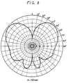
- the directivity on the vertical plane of the antenna in this embodiment is represented as shown in Fig. 8 in which the maximum gain is provided at the elevation angle of about 45 degrees.
- the elevation angles at which the maximum gain is provided are changed as about 50 degrees and 40 degrees as shown in Figs. 9 and 10, respectively.
- the main radiation beam of the microstrip antenna in this embodiment can cover the range of elevation angles of the geostationary satellite in the above-mentioned middle latitude area. Further, since the microstrip antenna in this embodiment is non-lateral directivity on the horizontal plane, this microstrip antenna is suitable for application to the mobile station in the wireless communication system utilizing the geostationary satellite.
- the main radiation beam can be directed to the underside by increasing the dielectric constant of the dielectric substrate 3.
- ground planar conductive element 1 is prepared in the separated form of the portion contacting with the dielectric substrate 3 and its peripheral portion, and they may be connected electrically and mechanically.
- microstrip antenna according to a second embodiment of the present invention will be described with reference to Figs. 11 and 12.
- a circular conductive element 13 having a middle-sized diameter is coaxially stacked on a circular ground planar conductive element 11 having a largest diameter via a dielectric layer 12 having a large diameter and made of a material such as fluoroplastics of low dielectric loss.
- a circular conductive element 15 having a small diameter is coaxially stacked on the circular conductive element 13 via a dielectric layer 14 having a small diameter.
- radiuses r11, r13 and r15 of the respective circular conductive elements 11, 13 and 15 are selected to be 90 mm, 55 mm and 26.5 mm, and dielectric constants ⁇ r and thicknesses t12 and t14 of the dielectric layers 12 and 14 are selected to be 2.6 and 3.2 mm, respectively.
- feed points 13f1 and 13f2 are respectively provided on the circular conductive element 13 having the middle-sized diameter at two positions equally offset from the center of the conductive element 13 by the distance r f and having an angular spacing ⁇ therebetween.
- a feed point 15f is provided at the center of the circular conductive element 15 having the small diameter.
- the feed points 13f1 and 13f2 of the circular conductive element 13 having the middle-sized diameter are respectively connected with coaxial feed lines 21 and 22.
- the outside conductor of the feed line 21 and the outside conductor 24 of the feed line 22 are both connected to the ground planar conductive element 11.
- the feed point 15f of the circular conductive element 15 having the small diameter is connected with an inside conductor 26 of a coaxial feed line 25, and an outside conductor 27 of the feed line 25 is connected to the ground planar conductive element 11.
- the middle-sized diameter circular conductive element 13 is electrically connected at its center to the ground planar conductive element 11 by a through-hole forming-process, whereby the outside conductor 27 of the coaxial feed line 25 is connected to the central portion of the middle-sized diameter circular conductive element 13.
- the circular conductive element 15 of a small diameter is fed at its center and its radius r15 is 26.5 mm, whereby it resonates at the frequency of 4.2 GHz in the TM01 mode and becomes a radiation element for radiating a vertically-polarized wave.
- the circular conductive element 13 functions as a ground planar conductive element relative to the circular conductive element 15 so that it provides a directivity on a vertical plane in which its main beam falls in a range of desired angle of elevation as shown in Fig. 13.
- the circular conductive element 13 resonates in the TM21 mode by a signal having a frequency of 1.6 GHz applied to the first feed point 13 f1 having the impedance of 50 ⁇ and at a reference phase (0 degree) and to the second feed point 13 f2 having the impedance 50 ⁇ and at a phase of -90 degrees.
- the circular conductive element 13 becomes a circular polarized wave radiation element which provides a desired directivity on a vertical plane as shown in Fig. 14.
- the operation of the microstrip antenna in this embodiment can be stabilized by connecting the central portion of the cicular conductive element 13 of a middle-sized diameter to the ground planar conductive element 11.
- the microstrip antenna is driven to emit a radiation wave of conical beam shape in which a desired directivity does not need the gain in the front direction, whereby the circumstance in the front direction hardly affects the characteristic of the microstrip antenna.
- the antenna for the high frequency band is stacked at the center of the antenna for the low frequency band, whereby a predetermined directivity can be provided by the microstrip antenna of small size and having a simplified arrangement according to this embodiment.
- the resonant frequency of the circular conductive element 13 of a middle-sized diameter is lowered by the influence of the upper dielectric layer 14 (see Fig. 12).
- the overall arrangement of the microstrip antenna system can be made more compact in size by utilizing a hybrid circuit 30 shown in Fig. 15.
- a copper foil 32 of a double-faced copper-bonded laminate layer 32 using fluoroplastics having a thickness of, for example, 0.8 mm is constructed as shown in Fig. 15 and the hybrid circuit 30 is supplied with a signal from its input terminal IN, then the left-hand side of the hybrid circuit 30 from its point A becomes symmetrical with respect to both the vertical and horizontal directions.
- the lengths of its portions of lines BC and BD are selected to be substantially 1/4 of the effective wavelength, and the signal power at the point A is equally divided and fed to two output terminals O1 and O2. Simultaneously, the phase of the signal at the output terminal O2 is delayed by 90 degrees.
- reference letter T designates a terminating resistor terminal.
- the hybrid circuit 30 is bonded back to back with the ground planar conductive element 11, whereby the corresponding output terminals and the feed points can be connected by conductor pins (not shown) with ease.
- the portion to be soldered is not exposed so that only the small diameter portion and the peripheral edge portion of the matching circuit can be soldered according to the normal soldering-process.
- the soldering-process is difficult to make.
- the connected portion of relatively large area can be soldered over the whole area by a reflowing-process utilizing a solder having a low melting point, which needs plenty of time. Also, there is presented such a problem that the fluctuation of relative positions of respective portions can not be restricted without difficulty.
- the microstrip antenna of the invention is driven in the SHF (super high frequency) band so that the length of the connection pin, which connects the feed point 15f of the small-diameter circular conductive element 15 and the antenna side terminal of the matching circuit, becomes important for the predetermined dimensions illustrated in the example of Fig. 6. Therefore, the disturbance of impedance at that portion exerts a bad influence upon a transmission characteristic.
- SHF super high frequency
- the hybrid or matching circuit 30 is comprised of a fluoroplastic layer 31 having a proper thickness, and a conductive element 32 forming one of a double-faced copper-bonding laminate layer and a conductive element 33 forming the other conductive element of the double-faced copper-bonding laminate layer, wherein the fluoroplastic layer 31 is interposed between the conductive elements 32 and 33, the conductive element 32 is employed as the ground planar conductive element and the conductive element 33 is arranged to have a predetermined pattern. The ground planar conductive element 32 is brought in contact with the ground planar conductive element 11 of the antenna.
- a screw 41 made of a conductive material extends from the center of the small-diameter circular conductive element 15 of the antenna through the inside of a through-hole conductive layer 17 formed between the middle-sized diameter circular conductive element 13 and the ground planar conductive element 11 so as to project to the underside of an antenna side terminal 30a of the matching circuit 30.
- a screw thread is threaded on the tip end portion of the screw 41 and is engaged with a nut 42 made of a conductive material, whereby the small-diameter portion and the large-diameter portion of the antenna and the matching circuit 30 are fastened together.
- the center of the small-diameter circular conductive element 15, i.e. the feed point and the antenna side terminal 30a of the matching circuit 30 are connected via the conductive screw 41 and the conductive nut 42.
- An inside conductor 26 of a semi-rigid coaxial feed line 25C is soldered to the other terminal of the matching circuit 30.
- An outside conductor 27 of this coaxial feed line 25C is soldered to the ground planar conductive element 11.
- the feed point 13f of the middle-sized diameter circular conductive element 13 is also connected to a phase difference feed circuit of strip line type by a feed pin, they are not shown for simplicity.
- the microstrip antenna since the microstrip antenna is constructed as described above, the central feed point of the small-diameter circular conductive element 15 of the antenna and the terminal 30a of the matching circuit 30 can be positively connected via the conductive screw 41 and the conductive nut 42. Simultaneously, the small diameter portion and the large diameter portion of the antenna and the matching circuit 30 can be coupled positively. Since the above three members are coupled by the screw 41 and the nut 42, they can be coupled with great ease, which provides an improved working efficiency.
- the central portion of the screw 41 and the through-hole conductive layer 17 constitute the coaxial line having the characteristic impedance of 50 ⁇ so that no trouble occurs relative to the matching circuit 30.
- the diameter d41 of the screw 41 and the inner diameter D17 of the through-hole conductive layer 17 are selected as D17/d41 ⁇ 3.2
- specific inductive capacity of fluoroplastics is selected as about 2.
- a conductive bonding agent is interposed between the two ground planar conductive elements 11 and 32 of the antenna and the matching circuit 30 and between the middle-sized diameter circular conductive element 13 and the small-diameter circular conductive element 16 of the antenna respectively, then mechanical strength of the antenna can be increased.
- the screw 41 and the nut 42 are used as the fastening members as described above, they may be replaced with a screw having threads on its respective ends and two nuts. In that event, if a nut having a large diameter is used, then it becomes possible to increase the pressing area.
- a conductive substrate 101 which is made of an aluminum plate whose thickness is, for example, 3 mm.
- a plurality of screw apertures 102 are formed through the conductive substrate 101, on its peripheral edge portion, and the ground planar conductive element 11 is brought in contact with one surface of the conductive substrate 101 and the antenna is then fixed thereto by inserting screws Sa into the apertures 102.
- Through-holes 103 and 105 are bored through the conductive substrate 101 in association with two feed points 13f1 and 13f2 of the middle-diameter circular conductive element 13 of the antenna and the feed point 15f of the small diameter circular conductive element 15 of the antenna, respectively.
- a hybrid circuit 30A is mounted on the other surface of the conductive substrate 101 by screws Sb while its ground planar conductive element 132 being brought in contact with the conductive substrate 101 as shown in Fig. 19.
- One output terminal 342 of the hybrid circuit 30A and one feed point 13f2 of the middle-sized diameter circular conductive element 13 are soldered to respective ends of a feed pin 104 which extends through the through-hole 103 of the conductive substrate 101, thus the output terminal 342 and the feed point 13f2 being connected to each other.
- the other feed point 13f1, though not shown, and an output terminal 341 are similarly connected.
- an inside conductor 123 of a semi-rigid coaxial feed line 22C is soldered to an input terminal 35 of the hybrid circuit 30A.
- the coaxial feed line 22C is secured to the conductive substrate 101 by a support metal fitting 107, screws Sc and the like.
- feed point 15f of the small-diameter conductive element 15 is also connected to the strip line type matching circuit by a feed pin 106 which extends through the through-hole 105 of the conductive substrate 101, this will not be shown in detail for simplicity.
- the microstrip antenna is constructed as described above, whereby the ground planar conductive element 11 of the antenna and the ground planar conductive element 132 of the hybrid circuit 30A are positively connected via the conductive substrate 101. Simultaneously, the outside conductor 124 of the coaxial feed line 22C and the ground planar conductive element 132 of the hybrid circuit 30A are positively connected in a like manner.
- the two ground planar conductive elements 11 and 132 are connected via the screws Sa, Sb and the conductive substrate 101 with great ease, which provides an improved working efficiency.
- the antenna and the hybrid circuit 30A are both provided with the ground planar conductive elements 11 and 132, the ground planar conductive elements 11 and 132 may be removed.
- the conductive substrate 101 light in weight by reducing the thickness of the conductive substrate 101 on its surface to which the hybrid circuit 30A is attached except its portions in contact with the hybrid circuit 30A and near the screw apertures 102 formed on the peripheral edge of the conductive substrate 101.
- the substrate 101 can reduce the thickness of its surface facing the antenna except its portions near the through-holes 103 and 105 and the screw aperture (not shown) for the screws Sb within the opposing area to the hybrid circuit 30A.
- the hybrid circuit 30A is the non-shield strip line type as described above, it might be a shield strip line type.
- a conductive housing 201 which is made of, for example, an aluminun.
- a plurality of screw apertures 202 are formed around the peripheral edge of the housing 201.
- a concave or recess portion 203 is formed on the central portion of the upper surface of the conductive housing 201, and a hybrid circuit 30S is accommodated within the recess 203.
- this hybrid circuit 30S is of a shield strip line type in which a pattern conductive element 233r is sandwiched between ground planar conductive elements 232 and 242 via dielectric layers 231 and 241.
- Fig. 20 is a diagrammatic view of section taken along the section line XX - XX in Fig. 21.
- the depth of the recess portion 203 of the conductive housing 201 is selected to be equal to the thickness of the hybrid circuit 30S, and the ground planar conductive element 11 is brought in contact with the upper ground planar conductive element 242 of the hybrid circuit 30S and the upper surface of the conductive housing 201, thus mounting the antenna by screws Sa.
- a coaxial connector 228 is secured to the under surface of the conductive housing 201 by screws Sb.
- the microstrip antenna is constructed as described above, whereby the ground planar conductive element 11 of the antenna and the two ground planar conductive elements 232 and 242 of the hybrid circuit 30S are positively connected via the conductive housing 201, and the outside conductor of the coaxial connector 228 and the two ground planar conductive elements 232 and 242 of the hybrid circuit 30S are positively connected in the same fashion.
- connection of the ground planar conductive elements 11, 232 and 242 is effected by the screws Sa, Sb and the conductive housing 201 with great ease, which provides an improved working efficiency.
- the hybrid circuit 30S includes the ground planar conductive elements 232 and 242 as described above, the ground planar conductive elements 232 and 242 might be removed. In that event, the bottom of the recess 203 of the conductive housing 201 and the ground planar conductive element 11 of the antenna are shielded.
- the under surface of the conductive housing 201 except the concave portion 203 accommodating the hybrid circuit 30S and the peripheral edge portion near the screw apertures 202 is properly reduced in thickness so that the weight of the microstrip antenna of the fifth embodiment can be reduced.
Description
- The present invention relates generally to microstrip antennas and more particularly to a microstrip antenna having a circular radiation element.
- It has been proposed that a wireless communication system is established between a base station and a number of mobile stations via a geostationary satellite (see Japanese Patent Application No. 63-331494).
- Fig. 1 shows such previously-proposed wireless communication system, in which a down channel between a base station CS and a number of mobile stations M is established via a geostationary satellite STd, while an up channel between the mobile stations M and the base station CS is established via a geostationary satellite STu. The frequencies of the up channel and the down channel are selected to be, for example, 1.6 GHz and 4.2 GHz, respectively. In this wireless communication system, a user HQ such as a transportation company and the base station CS are connected via another communication network line L, by way of example.
- In the above-noted wireless communication system, the mobile station M side utilizes a microstrip antenna because it is simple in construction and has a low physical profile.
- The microstrip antenna according to the prior art will be described with reference to Figs. 2 and 3.
- As shown in Figs. 2 and 3, a
circular radiation element 3 is laminated (i.e. stacked) on a rectangular ground plane conductor element 1 via adielectric element 2 made of a material such as fluoroplastics having a low dielectric loss. Afeed point 3f is located at the position offset from the center of thecircular radiation element 3, and is connected with an inside conductor 5 of acoaxial feed line 4.Reference numeral 6 designates an outside conductor forming thecoaxial feed line 4. - When the
circular radition element 3 in this microstrip antenna resonates in TM₁₁ mode (i.e. waveguide dominant mode), a surface current is distributed as shown by dashed lines in Fig. 2, and a directivity becomes unilateral in which a maximum gain is provided in the front direction. - In the mobile wireless communication system utilizing a geostationary satellite or the like, an elevation angle of geostationary satellite as seen from a mobile station falls within a range of from about 25 to 65 degrees in the area of middle latitude.
- When the prior-art microstrip antenna as described above is used in the mobile station side, the maximum gain direction of antenna and the elevation angle of geostationary satellite do not coincide with each other, degenerating the antenna gain.
- In order to obtain a desired directivity matched with the angle of elevation of the geostationary satellite, it is generally proposed to array microstrip antennas in which a plurality of microstrip antennas are properly connected to feed radiation elements with different phases.
- This type of microstrip array antenna is, however, increased in size and becomes complicated in structure.
- The mobile station side in the above-noted wireless communication system needs independent antennas respectively corresponding to the up channel and down channel.
- IEEE Transactions on Antennas and Propagation (Vol. 27, No. 3, pp. 270 to 273, published on March, 1978), for example, reports a two-frequency antenna in which a non-feed circular conductor element is coaxially stacked (i.e. laminated) on the
radiation element 3 of the prior-art microstrip antenna (shown in Figs. 2 and 3) via the dielectric element. - This two-frequency antenna can not cover two frequencies (1.6 GHz and 4.2 GHz) whose frequency ratio is very large, for example, about 1 : 2.6 as in the case where it is utilized in the afore-noted wireless commuication system.
- For a comprehensive study of microwave antennas, and microstrip antennas in particular, reference may be made to "Microstrip Antennas", by I. J. Bahl, P. Bhartia, Artech House, 1982, pp 86-96. The microstrip antennas disclosed therein comprise a low-loss dielectric layer sandwiched between a grounded planar element and an overlying circular radiation element. Various excitation modes are discussed.
- For an example of a microstrip antenna corresponding to the preamble of
claim 4, reference may be made to EP-A-0 188 087. - Finally, US-A-4 651 159 discloses a circularly polarized microstrip antenna in which a circular radiative element rests on a dielectric base which is separated from the antenna substrate by an air gap, the dielectric base being supported by spacer blocks. The air gap is intended to form an additional dielectric layer.
- Accordingly, it is an object of the present invention to provide an improved microstrip antenna which can eliminate the defects encountered with the prior art.
- It is another object of the present invention to provide a single microstrip antenna which has a directivity on a vertical plane in a range of a predetermined angle of elevation and has a non-directional radiation pattern on a horizontal plane.
- It is still another object of the present invention to provide a microstrip antenna of a simplified arrangement which has a directivity on a vertical plane in a range of a predetermined angle of elevation in a plurality of frequency bands apart from each other and has a non-directional radiation pattern on a horizontal plane.
- It is a further object of the present invention to provide a microstrip antenna in which a soldering-process for connecting a portion having a large area is not needed and an antenna and a feed system can be positively connected mechanically and electrically with ease by a simple structure.
- It is a yet further object of the present invention to provide a microstrip antenna which is thin in structure and in which the employment of a coaxial feed line and the soldering-process for connecting a portion having a large area are not needed, and an antenna, a feed circuit and a coaxial connector can be positively connected mechanically and electrically with ease.
- The above-noted objects are attained, according to the invention by a microstrip antenna as defined in
claims 1 and 4 - According to the arrangement defined in claim 1, the main radiation beam covers a vertically-polarized wave on a vertical plane in a range of a predetermined angle of elevation, and the microstrip antenna of the invention has a non-directional on a horizontal plane.
- According to the arrangement of
claim 4, the conductive circular element having the smallest diameter operates as a radiation element for the highest frequency band and other conductive circular elements operate as radiation elements for lower frequency bands as well as operate as ground planar conductive elements for adjacent smaller-diameter conductive circular elements, whereby the microstrip antenna of the invention is made small in size and simplified in structure and provides a directivity of a desired conical-beam shape over a plurality of frequency bands. - These and other objects, features and advantages of the present invention will be apparent from the following detailed description of preferred embodiments when read in conjunction with the accompanying drawings in which like reference numerals are used to identify the same or similar part in the several views.
-
- Fig. 1 is a pictorial and schematic representation of a mobile wireless communication system utilizing geostationary satellites according to the prior art;
- Fig. 2 is a top planar view of a microstrip antenna according to the prior art;
- Fig. 3 is a diagrammatic view of a section of the prior-art microstrip antenna, taken along line III - III of Fig. 2;
- Fig. 4 is a top planar view illustrating a microstrip antenna according to an embodiment of the present invention;
- Fig. 5 is a diagrammatic view of a section of the microstrip antenna, taken along line V - V of Fig. 4;
- Fig. 6 is a schematic diagram illustrating in cross-section a main component of the microstrip antenna according to the present invention;
- Fig. 7 is a schematic diagram to which reference will be made in explaining how the impedance of the microstrip antenna of the invention is changed with drive frequencies;
- Fig. 8 shows a typical H-plane radiation pattern for the microstrip antenna of the invention in which a diameter of a ground plane conductor is 160 mm;
- Fig. 9 shows a typical H-plane radiation pattern for the microstrip antenna of the invention in which the diameter of the ground plane conductor is 130 mm;
- Fig. 10 shows a typical H-plane radiation pattern for the microstrip antenna of the invention in which the diameter of the ground plane is 200 mm;
- Fig. 11 is a top planar view illustrating the microstrip antenna according to a second embodiment of the present invention;
- Fig. 12 is a diagrammatic view of a section of the microstrip antenna, taken along line XII - XII of Fig. 11;
- Fig. 13 shows a typical H-plane radiation pattern for the microstrip antenna of the second embodiment in which the radiation element is resonated at frequency of 4.2 GHz;
- Fig. 14 shows a typical H-plane radiation pattern for the microstrip antenna of the second embodiment in which the radiation element is resonated at frequency of 1.6 GHz;
- Fig. 15 is a schematic diagram showing a hybrid circuit used in the second embodiment of the microstrip antenna according to the present invention;
- Fig. 16 is a diagrammatic view of a section illustrating a microstrip antenna according to a third embodiment of the present invention;
- Fig. 17 is a top planar view of a main portion of the microstrip antenna, taken along line XVI - XVI of Fig. 16;
- Fig. 18 is a top planar view illustrating the microstrip antenna according to a fourth embodiment of the present invention;
- Fig. 19 is diagrammatic view of a section of the microstrip antenna, taken along line XVIII - XVIII of Fig. 18;
- Fig. 20 is a diagrammatic view of a section illustrating the microstrip antenna according to a fifth embodiment of the present invention; and
- Fig. 21 is a perspective view illustrating a hybrid circuit used in the microstrip strip antenna of Fig. 20 in the exploded state.
- A microstrip antenna according to an embodiment of the present invention will now be described with reference to Figs. 4 to 10.
- The arrangement of the embodiment of the present invention is represented in Figs. 4 and 5. In Figs. 4 and 5, like parts corresponding to those of Figs. 2 and 3 are marked with the same references and therefore need not be described fully.
- It will be seen in Figs. 4 and 5 that a circular ground planar conductive element 1 and a
circular radiation element 2 have interposed therebetween adielectric substrate 3 which has the same diameter as that of theradiation element 2 and which is made of a material such as fluoroplastics having a low dielectric loss. For example, the ground planar conductive element 1 has a diameter d₁ of 160 mm, and theradiation element 2 has a diameter d₂ of 53 mm. A thickness t3 ofdielectric substrate 3 is, for example, 1.6 mm and a dielectric constant εr ofdielectric substrate 3 is about 2.6. - In this embodiment, as shown in Figs. 4 and 5, a
feed point 2f is provided at the center of theradiation element 2, and animpedance matching device 10 is interposed between thefeed point 2f and acoaxial connector 4. - As shown in Fig. 6, the
impedance matching device 10 is formed by coaxially providing insideconductors external conductor 313. - An impedance Z₀ of the microstrip antenna in this embodiment is expressed, as will be discussed below, as follows when the drive frequency is 4.185 GHz.

In association with the above-noted impedance Z₀, diameters d₁₁ and d₁₂ ofinside conductors external conductor 313 is selected to be, for example, 2.3 mm. - A distant electric field of the circular microstrip antenna is generally expressed by the following equation (1) in a polar coordinate system in which the center of the radiation element assumes an original point.

where


- In the equation (1), Jn(x) represents the n-order Bessel function, a the radius of radiation element, t the thickness of dielectric substrate and λ the wavelength. Further, E₀ represents a constant.
- In the equation (1), only the terms of ϑ and φ represent the radiation pattern directivity of antenna so that, if they are represented as Dϑ and Dφ, they yield the following equation (2).

- When the circular microstrip antenna resonates in the TM0l mode, then n = 0 is established in the equation (l), accordingly, in the equation (2). Thus, the following equalities are satisfied.

Hence, this modifies the equation (2) as the following equation (3)
- Thus, when the microstrip antenna resonates in the TM₀₁ mode, the radiation electric field of the circular microstrip antenna contains only the ϑ component and the magnitude thereof is expressed by the function of only ϑ regardless of φ. In other words, the radiation electric field is a vertical polarized wave and has a non-directional on a horizontal plane.
- The radius a of the radiation element is expressed by the following equation (4).

where
In the equation (4), α represents a correction term for the thickness t of the dielectric element, and α is obtained experimentally. The thickness t of the dielectric element is determined in association with the radiation characteristic of the antenna. - The impedance seen from the feed point of the circular microstrip antenna is expressed by the following equation (5) where ρ assumes a distance between the center of the radiation element and the feed point.

- If ρ = 0, all values of Bessel function higher than one-order become zero, and only the 0-order Bessel function J₀(0) taken a finite value. That is, only when the radiation element resonates in the TM0l mode, the radiation element is fed at its center.
- Further, the surface current in this case is radially distributed from the central feed point to the peripheral edge as shown by dashed lines in Fig. 4 so that the directivity on the vertical plane can be prevented from being displaced unlike the case where the radiation element is fed at its feed point offset from its center.
- In this embodiment, let us assume that the diameters d₁ and d₂ of the ground planar conductive element 1 and the
radiation element 2 are 160 mm and 53 mm and that the thickness t₃ and the dielectric constant εr of thedielectric substrate 3 are 1.6 mm and 2.6, respectively. Then, when the drive frequency is 4.185 GHz, the impedances of the antenna in the TM0l mode in the non-existence of and in the existence of theimpedance matching device 10 are given by the following equations

- Thus, the impedances are varied in a range of frequency from 4.0 to 4.6 GHz as shown by solid and one-dot chain line curves Ls and La in Fig. 7.
- Further, calculating the radius of the radiation element from the equation (4) under the condition that x0l = 3.83171 and that f = 4.185 GHz yields

In practice, when the radius of theradiation element 2 is d₂/2 = 26.5 mm, theradiation element 2 resonates at the drive frequency, and a difference between the calculated radius and the radius in practice represents a correction amount α. - When the diameter d₁ of the ground planar conductive element 1 is 160 mm, the directivity on the vertical plane of the antenna in this embodiment is represented as shown in Fig. 8 in which the maximum gain is provided at the elevation angle of about 45 degrees.When the diameters d₁ of the ground planar conductive element 1 are 130 mm and 200 mm, the elevation angles at which the maximum gain is provided are changed as about 50 degrees and 40 degrees as shown in Figs. 9 and 10, respectively.
- As described above, the main radiation beam of the microstrip antenna in this embodiment can cover the range of elevation angles of the geostationary satellite in the above-mentioned middle latitude area. Further, since the microstrip antenna in this embodiment is non-lateral directivity on the horizontal plane, this microstrip antenna is suitable for application to the mobile station in the wireless communication system utilizing the geostationary satellite.
- Furthermore, the main radiation beam can be directed to the underside by increasing the dielectric constant of the
dielectric substrate 3. - In addition, the ground planar conductive element 1 is prepared in the separated form of the portion contacting with the
dielectric substrate 3 and its peripheral portion, and they may be connected electrically and mechanically. - The microstrip antenna according to a second embodiment of the present invention will be described with reference to Figs. 11 and 12.
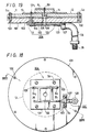
- As shown in Figs. 11 and 12, a circular
conductive element 13 having a middle-sized diameter is coaxially stacked on a circular ground planarconductive element 11 having a largest diameter via adielectric layer 12 having a large diameter and made of a material such as fluoroplastics of low dielectric loss. A circularconductive element 15 having a small diameter is coaxially stacked on the circularconductive element 13 via adielectric layer 14 having a small diameter. - In this embodiment, radiuses r₁₁, r₁₃ and r₁₅ of the respective circular
conductive elements dielectric layers - As shown in Fig. 11, feed points 13f₁ and 13f₂ are respectively provided on the circular
conductive element 13 having the middle-sized diameter at two positions equally offset from the center of theconductive element 13 by the distance rf and having an angular spacing ϑ therebetween. Afeed point 15f is provided at the center of the circularconductive element 15 having the small diameter. - In this embodiment, the offset distance rf of the feed points 13f1 and 13f2 and the angular spacing ϑ between the feed points 13f1 and 13f2 are respectively determined as rf = 33 mm, and ϑ = 135 degrees, by way of example.
- As shown in Fig. 12, the feed points 13f₁ and 13f₂ of the circular
conductive element 13 having the middle-sized diameter are respectively connected withcoaxial feed lines 21 and 22. The outside conductor of thefeed line 21 and the outside conductor 24 of the feed line 22 are both connected to the ground planarconductive element 11. - The
feed point 15f of the circularconductive element 15 having the small diameter is connected with aninside conductor 26 of acoaxial feed line 25, and anoutside conductor 27 of thefeed line 25 is connected to the ground planarconductive element 11. - In this embodiment, the middle-sized diameter circular
conductive element 13 is electrically connected at its center to the ground planarconductive element 11 by a through-hole forming-process, whereby theoutside conductor 27 of thecoaxial feed line 25 is connected to the central portion of the middle-sized diameter circularconductive element 13. - The operation of this embodiment will be described as follows.
- The circular
conductive element 15 of a small diameter is fed at its center and its radius r₁₅ is 26.5 mm, whereby it resonates at the frequency of 4.2 GHz in the TM₀₁ mode and becomes a radiation element for radiating a vertically-polarized wave. In that event, the circularconductive element 13 functions as a ground planar conductive element relative to the circularconductive element 15 so that it provides a directivity on a vertical plane in which its main beam falls in a range of desired angle of elevation as shown in Fig. 13. - The circular
conductive element 13, on the other hand, resonates in the TM₂₁ mode by a signal having a frequency of 1.6 GHz applied to thefirst feed point 13f1 having the impedance of 50Ω and at a reference phase (0 degree) and to thesecond feed point 13f2 having the impedance 50Ω and at a phase of -90 degrees. Thus, the circularconductive element 13 becomes a circular polarized wave radiation element which provides a desired directivity on a vertical plane as shown in Fig. 14. - Since the impedance at the center of the radiation element is fundamentally 0Ω in other modes than the TM₀₁ mode, in this embodiment, the operation of the microstrip antenna in this embodiment can be stabilized by connecting the central portion of the cicular
conductive element 13 of a middle-sized diameter to the ground planarconductive element 11. - In this embodiment, the microstrip antenna is driven to emit a radiation wave of conical beam shape in which a desired directivity does not need the gain in the front direction, whereby the circumstance in the front direction hardly affects the characteristic of the microstrip antenna. From this viewpoint, the antenna for the high frequency band is stacked at the center of the antenna for the low frequency band, whereby a predetermined directivity can be provided by the microstrip antenna of small size and having a simplified arrangement according to this embodiment.
- If the drive frequencies become close to each other, the resonant frequency of the circular
conductive element 13 of a middle-sized diameter is lowered by the influence of the upper dielectric layer 14 (see Fig. 12). - While in the second embodiment the feed points 13f1 and 13f2 of the circular
conductive element 13 of a middle-sized diameter are respectively supplied with the high frequency signals having the predetermined phase difference therebetween from thecoaxial feed lines 21 and 22 as described above, the overall arrangement of the microstrip antenna system can be made more compact in size by utilizing ahybrid circuit 30 shown in Fig. 15. - Referring to Fig. 15, if one
copper foil 32 of a double-faced copper-bondedlaminate layer 32 using fluoroplastics having a thickness of, for example, 0.8 mm is constructed as shown in Fig. 15 and thehybrid circuit 30 is supplied with a signal from its input terminal IN, then the left-hand side of thehybrid circuit 30 from its point A becomes symmetrical with respect to both the vertical and horizontal directions. The lengths of its portions of lines BC and BD are selected to be substantially 1/4 of the effective wavelength, and the signal power at the point A is equally divided and fed to two output terminals O₁ and O₂. Simultaneously, the phase of the signal at the output terminal O₂ is delayed by 90 degrees. In Fig. 15, reference letter T designates a terminating resistor terminal. If the distance between the two output terminals O₁ and O₂ is selected to be equal to the distance between the feed points 13f₁ and 13f₂ shown in Fig. 11, then thehybrid circuit 30 is bonded back to back with the ground planarconductive element 11, whereby the corresponding output terminals and the feed points can be connected by conductor pins (not shown) with ease. - When such a matching circuit and the small diameter portion of the above-noted antenna are formed from the double-faced copper-bonding laminate plate and are bonded to the ground planar
conductive element 11 and the middle-sized diameter circularconductive element 13, in order to more positively couple them mechanically and electrically, it is usual that the other small-diameter circular conductive element of the small diameter portion of the antenna is soldered to the middle-sized diameter circularconductive element 13 and the ground planar conductive element of the matching circuit is soldered to the ground planarconductive element 11 of the antenna. - In that event, the portion to be soldered is not exposed so that only the small diameter portion and the peripheral edge portion of the matching circuit can be soldered according to the normal soldering-process. Thus, the soldering-process is difficult to make.
- The connected portion of relatively large area can be soldered over the whole area by a reflowing-process utilizing a solder having a low melting point, which needs plenty of time. Also, there is presented such a problem that the fluctuation of relative positions of respective portions can not be restricted without difficulty.
- Further, the microstrip antenna of the invention is driven in the SHF (super high frequency) band so that the length of the connection pin, which connects the
feed point 15f of the small-diameter circularconductive element 15 and the antenna side terminal of the matching circuit, becomes important for the predetermined dimensions illustrated in the example of Fig. 6. Therefore, the disturbance of impedance at that portion exerts a bad influence upon a transmission characteristic. - In a third embodiment of the present invention, as shown in Fig. 16, the hybrid or matching
circuit 30 is comprised of afluoroplastic layer 31 having a proper thickness, and aconductive element 32 forming one of a double-faced copper-bonding laminate layer and aconductive element 33 forming the other conductive element of the double-faced copper-bonding laminate layer, wherein thefluoroplastic layer 31 is interposed between theconductive elements conductive element 32 is employed as the ground planar conductive element and theconductive element 33 is arranged to have a predetermined pattern. The ground planarconductive element 32 is brought in contact with the ground planarconductive element 11 of the antenna. - Further, as shown in Fig. 16, a
screw 41 made of a conductive material extends from the center of the small-diameter circularconductive element 15 of the antenna through the inside of a through-holeconductive layer 17 formed between the middle-sized diameter circularconductive element 13 and the ground planarconductive element 11 so as to project to the underside of anantenna side terminal 30a of the matchingcircuit 30. - In the intermediate portion of the
screw 41, its diameter d₄₁ and the inner diameter D₁₇ of through-hole conductive layer 17 (refer to Fig. 17) are selected so as to satisfy the following equation (6)
The intermediate portion of thescrew 41 and the through-holeconductive layer 17 provided as the outside conductor constitute a coaxial line whose characteristic impedance is 50Ω. - As shown in Fig. 16, a screw thread is threaded on the tip end portion of the
screw 41 and is engaged with anut 42 made of a conductive material, whereby the small-diameter portion and the large-diameter portion of the antenna and thematching circuit 30 are fastened together. Thus, the center of the small-diameter circularconductive element 15, i.e. the feed point and theantenna side terminal 30a of the matchingcircuit 30 are connected via theconductive screw 41 and theconductive nut 42. Aninside conductor 26 of a semi-rigidcoaxial feed line 25C is soldered to the other terminal of the matchingcircuit 30. Anoutside conductor 27 of thiscoaxial feed line 25C is soldered to the ground planarconductive element 11. - Although the
feed point 13f of the middle-sized diameter circularconductive element 13 is also connected to a phase difference feed circuit of strip line type by a feed pin, they are not shown for simplicity. - In the third embodiment, since the microstrip antenna is constructed as described above, the central feed point of the small-diameter circular
conductive element 15 of the antenna and the terminal 30a of the matchingcircuit 30 can be positively connected via theconductive screw 41 and theconductive nut 42. Simultaneously, the small diameter portion and the large diameter portion of the antenna and thematching circuit 30 can be coupled positively. Since the above three members are coupled by thescrew 41 and thenut 42, they can be coupled with great ease, which provides an improved working efficiency. - Further, the central portion of the
screw 41 and the through-holeconductive layer 17 constitute the coaxial line having the characteristic impedance of 50Ω so that no trouble occurs relative to thematching circuit 30. In addition, it is possible to determine the dimensions of the respective portions of the matchingcircuit 30 including the through-hole portion. - While in the third embodiment a dielectric element is not provided inside of the through-hole
conductive layer 17 and air exists therein as described above, if a spacer made of fluoroplastics is filled inside of the through-holeconductive layer 17, it is possible to restrict the position of thescrew 41 more accurately. - In this case, the diameter d₄₁ of the
screw 41 and the inner diameter D₁₇ of the through-holeconductive layer 17 are selected as
In the foregoing, specific inductive capacity of fluoroplastics is selected as about 2. - Further, if a conductive bonding agent is interposed between the two ground planar
conductive elements matching circuit 30 and between the middle-sized diameter circularconductive element 13 and the small-diameter circularconductive element 16 of the antenna respectively, then mechanical strength of the antenna can be increased. - Furthermore, while in the third embodiment the
screw 41 and thenut 42 are used as the fastening members as described above, they may be replaced with a screw having threads on its respective ends and two nuts. In that event, if a nut having a large diameter is used, then it becomes possible to increase the pressing area. - A fourth embodiment of the present invention will be described hereinbelow with reference to Figs. 18 and 19.
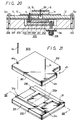
- Referring to Figs. 18 and 19, there is shown a
conductive substrate 101 which is made of an aluminum plate whose thickness is, for example, 3 mm. A plurality ofscrew apertures 102 are formed through theconductive substrate 101, on its peripheral edge portion, and the ground planarconductive element 11 is brought in contact with one surface of theconductive substrate 101 and the antenna is then fixed thereto by inserting screws Sa into theapertures 102. Through-holes conductive substrate 101 in association with two feed points 13f₁ and 13f₂ of the middle-diameter circularconductive element 13 of the antenna and thefeed point 15f of the small diameter circularconductive element 15 of the antenna, respectively. - A
hybrid circuit 30A is mounted on the other surface of theconductive substrate 101 by screws Sb while its ground planarconductive element 132 being brought in contact with theconductive substrate 101 as shown in Fig. 19. Oneoutput terminal 34₂ of thehybrid circuit 30A and one feed point 13f₂ of the middle-sized diameter circularconductive element 13 are soldered to respective ends of afeed pin 104 which extends through the through-hole 103 of theconductive substrate 101, thus theoutput terminal 34₂ and the feed point 13f₂ being connected to each other. The other feed point 13f₁, though not shown, and anoutput terminal 34₁ are similarly connected. As shown in Figs. 18 and 19, aninside conductor 123 of a semi-rigidcoaxial feed line 22C is soldered to aninput terminal 35 of thehybrid circuit 30A. Thecoaxial feed line 22C is secured to theconductive substrate 101 by a support metal fitting 107, screws Sc and the like. - While the
feed point 15f of the small-diameterconductive element 15 is also connected to the strip line type matching circuit by afeed pin 106 which extends through the through-hole 105 of theconductive substrate 101, this will not be shown in detail for simplicity. - According to the fourth embodiment, the microstrip antenna is constructed as described above, whereby the ground planar
conductive element 11 of the antenna and the ground planarconductive element 132 of thehybrid circuit 30A are positively connected via theconductive substrate 101. Simultaneously, theoutside conductor 124 of thecoaxial feed line 22C and the ground planarconductive element 132 of thehybrid circuit 30A are positively connected in a like manner. - The two ground planar
conductive elements conductive substrate 101 with great ease, which provides an improved working efficiency. - While in the fourth embodiment the antenna and the
hybrid circuit 30A are both provided with the ground planarconductive elements conductive elements - Further, it is possible to make the
conductive substrate 101 light in weight by reducing the thickness of theconductive substrate 101 on its surface to which thehybrid circuit 30A is attached except its portions in contact with thehybrid circuit 30A and near thescrew apertures 102 formed on the peripheral edge of theconductive substrate 101. - Further, when the antenna is provided with the ground planar
conductive element 11, thesubstrate 101 can reduce the thickness of its surface facing the antenna except its portions near the through-holes hybrid circuit 30A. - While in the fourth embodiment the
hybrid circuit 30A is the non-shield strip line type as described above, it might be a shield strip line type. - A fifth embodiment of the present invention will be described with reference to Figs. 20 and 21.
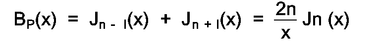
- Referring to Fig. 20, there is provided a
conductive housing 201 which is made of, for example, an aluminun. A plurality ofscrew apertures 202 are formed around the peripheral edge of thehousing 201. A concave orrecess portion 203 is formed on the central portion of the upper surface of theconductive housing 201, and ahybrid circuit 30S is accommodated within therecess 203. - As shown in Fig. 21 forming an exploded view of the fifth embodiment, this
hybrid circuit 30S is of a shield strip line type in which a patternconductive element 233r is sandwiched between ground planarconductive elements dielectric layers - The pattern
conductive element 233r in Fig. 21 and the patternconductive element 133 in Fig. 18 are placed in an inside and outside relationship. Further, Fig. 20 is a diagrammatic view of section taken along the section line XX - XX in Fig. 21. - The depth of the
recess portion 203 of theconductive housing 201 is selected to be equal to the thickness of thehybrid circuit 30S, and the ground planarconductive element 11 is brought in contact with the upper ground planarconductive element 242 of thehybrid circuit 30S and the upper surface of theconductive housing 201, thus mounting the antenna by screws Sa. - A
coaxial connector 228 is secured to the under surface of theconductive housing 201 by screws Sb. - The microstrip antenna of this embodiment is assembled in the following order:
- (1) The
coaxial connector 228 is secured to the under surface of theconductive housing 201 by the screws Sb; - (2) The main portion of the
hybrid circuit 30S, i.e. the portion below itspattern conductor 233r is located within therecess 203 of the upper surface of theconductive housing 201 under the condition that the ground planarconductive element 232 is directed downward, and theinput terminal 35 of the patternconductive element 233r and the inside conductor of thecoaxial connector 228 are soldered to each other; - (3) Pins 4₁ and 4₂ are respectively implanted on and soldered to
output terminals conductive element 233r; - (4) The
dielectric layer 241 and the ground planarconductive element 242 are mounted on the patternconductive element 233r, and thepins holes - (5) When the antenna is mounted on the upper surface of the
conductive housing 201 by screws, the upper ground planarconductive element 242 of thehybrid circuit 30S comes in contact with the ground planarconductive element 11 of the antenna, and thepins conductive element 11 and thedielectric layer 12 of the antenna and are exposed on feed points 13f₁ and 13f₂ of the middle-sized diameter circularconductive element 13; and - (6) The feed points 13f₁ and 13f₂ are soldered to the corresponding pins 4₁ and 4₂, respectively.
- According to the fifth embodiment, the microstrip antenna is constructed as described above, whereby the ground planar
conductive element 11 of the antenna and the two ground planarconductive elements hybrid circuit 30S are positively connected via theconductive housing 201, and the outside conductor of thecoaxial connector 228 and the two ground planarconductive elements hybrid circuit 30S are positively connected in the same fashion. - The connection of the ground planar
conductive elements conductive housing 201 with great ease, which provides an improved working efficiency. - While in the fifth embodiment the
hybrid circuit 30S includes the ground planarconductive elements conductive elements recess 203 of theconductive housing 201 and the ground planarconductive element 11 of the antenna are shielded. - Further, it is also possible to remove both the
dielectric layer 241 and the ground planarconductive element 242 which are provided above the patternconductive element 233r. In that event, the main portions of the patternconductive element 233r side are properly secured to theconductive housing 201 by screws and the like. Also, the predetermined dimension of the pattern of the patternconductive element 233r is slightly increased. - Further, the under surface of the
conductive housing 201 except theconcave portion 203 accommodating thehybrid circuit 30S and the peripheral edge portion near thescrew apertures 202 is properly reduced in thickness so that the weight of the microstrip antenna of the fifth embodiment can be reduced. - While in the above-mentioned embodiments two frequency bands are employed, the present invention can be similarly applied to the case where three frequency bands or more are employed.
Claims (9)
- A microstrip antenna having directivity in a vertical plane in a range of predetermined angles of elevation and a non-directional radiation pattern in a horizontal plane, suitable for establishing an up channel and a down channel with a geostationary satellite, comprising:- a grounded conductive planar element (1; 11);- a radiation element of substantially circular shape (2; 15);- a dielectric layer (3; 14) having a small dielectric loss and provided between said planar element (1; 11) and said radiation element (2; 15); and- feed means (4, 10; 25) connected to a feed point of said radiation element
characterized in that said feed point is connected at the centre of said radiation element (2, 15) so that said radiation element is resonated in the TM₀₁ mode, whereby said directivity in a vertical plane is obtained. - A microstrip antenna according to claim 1, wherein said feed means (4, 10; 25) includes impedance matching means (10).
- A microstrip antenna according to claim 2, wherein said impedance matching means (10) includes an inside conductor (26) connected to said feed point and an outside conductor (27) connected to said conductive planar element, and said inside conductor and said outside conductor are coaxially arranged.
- A microstrip antenna comprising:(i) a grounded conductive planar element (11);(ii) a plurality of conductive circular elements (13, 15) each being coaxially stacked on said grounded conductive planar element with an intermediate dielectric layer (12, 14) having a small dielectric loss in the sequential order of diameters thereof;(iii) a feed point (25) located at the centre of said conductive circular element (15) having the minimum diameter;
characterized in that it further comprises:(iv) feed points (21, 22) provided on said other conductive circular elements (13) at positions offset from their centres, wherein said conductive circular element having the minimum diameter (15) is resonated in the TM₀₁ mode. - A microstrip antenna according to claim 4, further comprising first feed means (26) connected to the feed point of said conductive circular element (15) having the minimum diameter and second feed means (21, 23) connected to the feed points of said other conductive circular elements.
- A microstrip antenna according to claim 5, wherein said first feed means includes an inside conductor (26) connected to said feed point (25) of said conductive circular element (15) having the minimum diameter, and an outside conductor (27) connected respectively to said other conductive circular elements (11, 13), said inside conductor and said outside conductor being coaxially arranged.
- A microstrip antenna according to claim 5, wherein said first feed means includes a conductive fastening member (41) extended from the underside of said conductive planar element (11) to substantially a centre of said conductive circular element (15) having the minimum diameter, said conductive circular element having the minimum diameter being fed through said fastening member.
- A microstrip antenna according to claim 5, wherein said second feed means includes a strip line type feed circuit (13f) mounted to said conductive circular element (13) having the maximum diameter on its surface opposite to a surface to which said conductive circular elements are stacked through a conductive substrate, and an output terminal of said feed circuit and the feed point provided on said conductive circular element are connected through said conductive substrate (11).
- A microstrip antenna according to claim 5, wherein said second feed means includes a conductive housing (201) in which a shield strip line type feed circuit is accommodated within a recess formed on one surface of said conductive housing and said one surface is mounted on a surface of said conductive planar element opposite to its surface on which said conductive circular elements are stacked, and a coaxial connector (228) mounted on the other surface of said conductive housing, wherein said coaxial connector and an input terminal of said feed circuit are connected via said conductive housing, and an output terminal of said feed circuit and the feed point of said antenna are connected together.
Applications Claiming Priority (10)
| Application Number | Priority Date | Filing Date | Title |
|---|---|---|---|
| JP24649088A JPH0294905A (en) | 1988-09-30 | 1988-09-30 | Microstrip antenna |
| JP246490/88 | 1988-09-30 | ||
| JP33149488A JPH02179102A (en) | 1988-12-29 | 1988-12-29 | Microstrip antenna |
| JP331494/88 | 1988-12-29 | ||
| JP1021173A JP2751304B2 (en) | 1989-01-31 | 1989-01-31 | Antenna feeder |
| JP1021172A JP2751303B2 (en) | 1989-01-31 | 1989-01-31 | Antenna feeder |
| JP21173/89 | 1989-01-31 | ||
| JP21172/89 | 1989-01-31 | ||
| JP1174789U JPH02103909U (en) | 1989-02-02 | 1989-02-02 | |
| JP11747/89 | 1989-02-02 |
Publications (3)
| Publication Number | Publication Date |
|---|---|
| EP0362079A2 EP0362079A2 (en) | 1990-04-04 |
| EP0362079A3 EP0362079A3 (en) | 1991-05-08 |
| EP0362079B1 true EP0362079B1 (en) | 1994-11-09 |
Family
ID=27519325
Family Applications (1)
| Application Number | Title | Priority Date | Filing Date |
|---|---|---|---|
| EP89402694A Expired - Lifetime EP0362079B1 (en) | 1988-09-30 | 1989-09-29 | Microstrip antenna |
Country Status (4)
| Country | Link |
|---|---|
| US (1) | US5121127A (en) |
| EP (1) | EP0362079B1 (en) |
| AU (1) | AU623437B2 (en) |
| DE (1) | DE68919323T2 (en) |
Families Citing this family (82)
| Publication number | Priority date | Publication date | Assignee | Title |
|---|---|---|---|---|
| US4987421A (en) * | 1988-06-09 | 1991-01-22 | Mitsubishi Denki Kabushiki Kaisha | Microstrip antenna |
| AU642756B2 (en) * | 1990-07-30 | 1993-10-28 | Sony Corporation | A matching device for a microstrip antenna |
| US5153600A (en) * | 1991-07-01 | 1992-10-06 | Ball Corporation | Multiple-frequency stacked microstrip antenna |
| DE4135828A1 (en) * | 1991-10-30 | 1993-05-06 | Deutsche Forschungsanstalt Fuer Luft- Und Raumfahrt E.V., 5300 Bonn, De | ANTENNA ARRANGEMENT |
| US5349288A (en) * | 1992-09-04 | 1994-09-20 | Miller John S | Radial planar current detection device having an extended frequency range of response |
| SE9404238L (en) * | 1994-12-07 | 1996-06-08 | Saab Ericsson Space Ab | Light weight antenna element |
| DE19514556A1 (en) * | 1995-04-20 | 1996-10-24 | Fuba Automotive Gmbh | Combined flat antenna for vehicle global positioning system and mobile radio |
| DE19546010A1 (en) * | 1995-12-09 | 1997-06-12 | Fuba Automotive Gmbh | Combined flat antenna for vehicle global positioning system and mobile radio |
| DE59501555D1 (en) * | 1995-04-20 | 1998-04-09 | Fuba Automotive Gmbh | Flat antenna arrangement |
| US5777583A (en) * | 1995-04-26 | 1998-07-07 | International Business Machines Corporation | High gain broadband planar antenna |
| US5864318A (en) * | 1996-04-26 | 1999-01-26 | Dorne & Margolin, Inc. | Composite antenna for cellular and gps communications |
| JPH1028012A (en) * | 1996-07-12 | 1998-01-27 | Harada Ind Co Ltd | Planar antenna |
| US5815119A (en) * | 1996-08-08 | 1998-09-29 | E-Systems, Inc. | Integrated stacked patch antenna polarizer circularly polarized integrated stacked dual-band patch antenna |
| DE19646100A1 (en) * | 1996-11-08 | 1998-05-14 | Fuba Automotive Gmbh | Flat antenna |
| EP1007308B1 (en) | 1997-02-24 | 2003-11-12 | Superior Micropowders LLC | Aerosol method and apparatus, particulate products, and electronic devices made therefrom |
| US6338809B1 (en) * | 1997-02-24 | 2002-01-15 | Superior Micropowders Llc | Aerosol method and apparatus, particulate products, and electronic devices made therefrom |
| US5940037A (en) * | 1997-04-29 | 1999-08-17 | The Whitaker Corporation | Stacked patch antenna with frequency band isolation |
| US6014114A (en) * | 1997-09-19 | 2000-01-11 | Trimble Navigation Limited | Antenna with stepped ground plane |
| DE19823749C2 (en) * | 1998-05-27 | 2002-07-11 | Kathrein Werke Kg | Dual polarized multi-range antenna |
| US20030148024A1 (en) * | 2001-10-05 | 2003-08-07 | Kodas Toivo T. | Low viscosity precursor compositons and methods for the depositon of conductive electronic features |
| DE69806765T2 (en) * | 1998-10-27 | 2003-04-24 | Bosch Gmbh Robert | Radiation diagrams for mobile phones |
| FR2785451B1 (en) * | 1998-11-04 | 2007-05-11 | Thomson Csf | MULTIFUNCTION PRINTED ANTENNA |
| US6087990A (en) * | 1999-02-02 | 2000-07-11 | Antenna Plus, Llc | Dual function communication antenna |
| DE10012809A1 (en) | 2000-03-16 | 2001-09-27 | Kathrein Werke Kg | Dual polarized dipole array antenna has supply cable fed to supply point on one of two opposing parallel dipoles, connecting cable to supply point on opposing dipole |
| DE10064129B4 (en) | 2000-12-21 | 2006-04-20 | Kathrein-Werke Kg | Antenna, in particular mobile radio antenna |
| US20030048226A1 (en) * | 2001-01-31 | 2003-03-13 | Tantivy Communications, Inc. | Antenna for array applications |
| US6369770B1 (en) | 2001-01-31 | 2002-04-09 | Tantivy Communications, Inc. | Closely spaced antenna array |
| US6396456B1 (en) | 2001-01-31 | 2002-05-28 | Tantivy Communications, Inc. | Stacked dipole antenna for use in wireless communications systems |
| US6417806B1 (en) | 2001-01-31 | 2002-07-09 | Tantivy Communications, Inc. | Monopole antenna for array applications |
| US6369771B1 (en) | 2001-01-31 | 2002-04-09 | Tantivy Communications, Inc. | Low profile dipole antenna for use in wireless communications systems |
| US7629017B2 (en) * | 2001-10-05 | 2009-12-08 | Cabot Corporation | Methods for the deposition of conductive electronic features |
| US6951666B2 (en) * | 2001-10-05 | 2005-10-04 | Cabot Corporation | Precursor compositions for the deposition of electrically conductive features |
| US7524528B2 (en) * | 2001-10-05 | 2009-04-28 | Cabot Corporation | Precursor compositions and methods for the deposition of passive electrical components on a substrate |
| US20060159838A1 (en) * | 2005-01-14 | 2006-07-20 | Cabot Corporation | Controlling ink migration during the formation of printable electronic features |
| US20030108664A1 (en) * | 2001-10-05 | 2003-06-12 | Kodas Toivo T. | Methods and compositions for the formation of recessed electrical features on a substrate |
| DE10150150B4 (en) | 2001-10-11 | 2006-10-05 | Kathrein-Werke Kg | Dual polarized antenna array |
| WO2003035279A1 (en) | 2001-10-19 | 2003-05-01 | Superior Micropowders Llc | Tape compositions for the deposition of electronic features |
| US7553512B2 (en) * | 2001-11-02 | 2009-06-30 | Cabot Corporation | Method for fabricating an inorganic resistor |
| US6850191B1 (en) | 2001-12-11 | 2005-02-01 | Antenna Plus, Llc | Dual frequency band communication antenna |
| JP3875568B2 (en) * | 2002-02-05 | 2007-01-31 | 株式会社東芝 | Semiconductor device and manufacturing method thereof |
| US6639558B2 (en) * | 2002-02-06 | 2003-10-28 | Tyco Electronics Corp. | Multi frequency stacked patch antenna with improved frequency band isolation |
| US20040021606A1 (en) * | 2002-07-11 | 2004-02-05 | Alps Electric Co., Ltd. | Small plane antenna and composite antenna using the same |
| US6950066B2 (en) * | 2002-08-22 | 2005-09-27 | Skycross, Inc. | Apparatus and method for forming a monolithic surface-mountable antenna |
| JP4052967B2 (en) * | 2003-03-25 | 2008-02-27 | 富士通株式会社 | Antenna coupling module |
| SE0301980D0 (en) * | 2003-07-03 | 2003-07-03 | St Jude Medical | Implantable medical device |
| US7372411B2 (en) * | 2004-06-28 | 2008-05-13 | Nokia Corporation | Antenna arrangement and method for making the same |
| DE102004035064A1 (en) * | 2004-07-20 | 2006-02-16 | Receptec Gmbh | antenna module |
| SE528084C2 (en) * | 2004-11-30 | 2006-08-29 | Powerwave Technologies Sweden | Double band antenna feed |
| US7575621B2 (en) | 2005-01-14 | 2009-08-18 | Cabot Corporation | Separation of metal nanoparticles |
| US8383014B2 (en) | 2010-06-15 | 2013-02-26 | Cabot Corporation | Metal nanoparticle compositions |
| WO2006076608A2 (en) | 2005-01-14 | 2006-07-20 | Cabot Corporation | A system and process for manufacturing custom electronics by combining traditional electronics with printable electronics |
| US20070190298A1 (en) * | 2005-01-14 | 2007-08-16 | Cabot Corporation | Security features, their use and processes for making them |
| WO2006076609A2 (en) | 2005-01-14 | 2006-07-20 | Cabot Corporation | Printable electronic features on non-uniform substrate and processes for making same |
| US8334464B2 (en) | 2005-01-14 | 2012-12-18 | Cabot Corporation | Optimized multi-layer printing of electronics and displays |
| US7824466B2 (en) | 2005-01-14 | 2010-11-02 | Cabot Corporation | Production of metal nanoparticles |
| JP2006319867A (en) * | 2005-05-16 | 2006-11-24 | Matsushita Electric Ind Co Ltd | Antenna module and wireless device using it |
| US7545333B2 (en) * | 2006-03-16 | 2009-06-09 | Agc Automotive Americas R&D | Multiple-layer patch antenna |
| EP2052462A4 (en) * | 2006-08-01 | 2009-08-12 | Agency Science Tech & Res | Antenna for near field and far field radio frequency identification |
| US8111196B2 (en) * | 2006-09-15 | 2012-02-07 | Laird Technologies, Inc. | Stacked patch antennas |
| US7277056B1 (en) * | 2006-09-15 | 2007-10-02 | Laird Technologies, Inc. | Stacked patch antennas |
| US7492319B2 (en) * | 2006-09-22 | 2009-02-17 | Laird Technologies, Inc. | Antenna assemblies including standard electrical connections and captured retainers and fasteners |
| JP5054569B2 (en) * | 2008-02-28 | 2012-10-24 | 富士通コンポーネント株式会社 | connector |
| ITPD20080132A1 (en) | 2008-04-29 | 2009-10-30 | Calearo Antenne Spa | MODULE OF MULTIFUNCTIONAL ANTENNA FOR THE TREATMENT OF A MULTIPLICITY OF SIGNALS IN RADIO FREQUENCY. |
| TWI381585B (en) * | 2009-06-30 | 2013-01-01 | Wistron Neweb Corp | Dual antenna device |
| JP4818443B2 (en) * | 2009-12-24 | 2011-11-16 | 株式会社東芝 | Coupler device |
| US20110163921A1 (en) | 2010-01-06 | 2011-07-07 | Psion Teklogix Inc. | Uhf rfid internal antenna for handheld terminals |
| JP4875176B2 (en) * | 2010-02-19 | 2012-02-15 | 株式会社東芝 | Antenna and coupler |
| JP4988017B2 (en) * | 2010-07-23 | 2012-08-01 | 株式会社東芝 | Coupler device and information processing device |
| US8669903B2 (en) | 2010-11-09 | 2014-03-11 | Antenna Plus, Llc | Dual frequency band communication antenna assembly having an inverted F radiating element |
| US9196959B1 (en) * | 2010-12-23 | 2015-11-24 | Rockwell Collins, Inc. | Multi-ring switched parasitic array for improved antenna gain |
| US9024831B2 (en) * | 2011-05-26 | 2015-05-05 | Wang-Electro-Opto Corporation | Miniaturized ultra-wideband multifunction antenna via multi-mode traveling-waves (TW) |
| CN103259085B (en) * | 2013-05-02 | 2015-11-25 | 深圳市华信天线技术有限公司 | A kind of combined antenna and hand held antenna device |
| US9548541B2 (en) * | 2015-03-30 | 2017-01-17 | Huawei Technologies Canada Co., Ltd. | Apparatus and method for a high aperture efficiency broadband antenna element with stable gain |
| US10109918B2 (en) * | 2016-01-22 | 2018-10-23 | Airgain Incorporated | Multi-element antenna for multiple bands of operation and method therefor |
| CN107395788B (en) * | 2016-05-17 | 2021-03-23 | 北京小米移动软件有限公司 | Terminal shell and terminal |
| JP6833523B2 (en) * | 2017-01-11 | 2021-02-24 | 株式会社デンソーテン | Microstrip antenna |
| KR101989820B1 (en) * | 2017-03-14 | 2019-06-18 | 주식회사 아모텍 | Multilayer patch antenna |
| TWI689130B (en) * | 2017-08-02 | 2020-03-21 | 佳邦科技股份有限公司 | Portable electronic device and stacked antenna module thereof |
| JP2020120262A (en) * | 2019-01-23 | 2020-08-06 | ソニーセミコンダクタソリューションズ株式会社 | Antenna and millimeter wave sensor |
| CN112400255B (en) * | 2019-04-24 | 2023-06-27 | 株式会社村田制作所 | Antenna module and communication device equipped with the same |
| CN112751178A (en) * | 2019-10-29 | 2021-05-04 | 北京小米移动软件有限公司 | Antenna unit, array antenna and electronic equipment |
| US11502414B2 (en) * | 2021-01-29 | 2022-11-15 | Eagle Technology, Llc | Microstrip patch antenna system having adjustable radiation pattern shapes and related method |
Family Cites Families (11)
| Publication number | Priority date | Publication date | Assignee | Title |
|---|---|---|---|---|
| US3545002A (en) * | 1969-02-04 | 1970-12-01 | Sperry Rand Corp | Wideband wave trapping antenna having a time limited impulse response |
| GB2054275B (en) * | 1979-07-12 | 1983-07-06 | Emi Ltd | Antenna |
| JPS6036642B2 (en) * | 1980-08-04 | 1985-08-21 | 沖電気工業株式会社 | antenna |
| JPS5829203A (en) * | 1981-08-17 | 1983-02-21 | Nippon Telegr & Teleph Corp <Ntt> | Multilayered microstrip diversity antenna |
| US4401988A (en) * | 1981-08-28 | 1983-08-30 | The United States Of America As Represented By The Secretary Of The Navy | Coupled multilayer microstrip antenna |
| EP0117017A1 (en) * | 1983-01-20 | 1984-08-29 | Hazeltine Corporation | Low-profile omni-antenna |
| US4651159A (en) * | 1984-02-13 | 1987-03-17 | University Of Queensland | Microstrip antenna |
| US4660048A (en) * | 1984-12-18 | 1987-04-21 | Texas Instruments Incorporated | Microstrip patch antenna system |
| JPS6248103A (en) * | 1985-08-27 | 1987-03-02 | Matsushita Electric Works Ltd | Microstrip line antenna |
| GB8531859D0 (en) * | 1985-12-30 | 1986-02-05 | British Gas Corp | Broadband antennas |
| US4827271A (en) * | 1986-11-24 | 1989-05-02 | Mcdonnell Douglas Corporation | Dual frequency microstrip patch antenna with improved feed and increased bandwidth |
-
1989
- 1989-09-25 US US07/412,167 patent/US5121127A/en not_active Expired - Lifetime
- 1989-09-29 DE DE68919323T patent/DE68919323T2/en not_active Expired - Lifetime
- 1989-09-29 EP EP89402694A patent/EP0362079B1/en not_active Expired - Lifetime
- 1989-09-29 AU AU42435/89A patent/AU623437B2/en not_active Expired
Non-Patent Citations (1)
| Title |
|---|
| I.J. Bahl, P. Bhartia, "Microstrip Antennas", 1982, Artech House, pages 86-96. * |
Also Published As
| Publication number | Publication date |
|---|---|
| AU623437B2 (en) | 1992-05-14 |
| AU4243589A (en) | 1990-04-05 |
| DE68919323T2 (en) | 1995-04-06 |
| DE68919323D1 (en) | 1994-12-15 |
| EP0362079A2 (en) | 1990-04-04 |
| US5121127A (en) | 1992-06-09 |
| EP0362079A3 (en) | 1991-05-08 |
Similar Documents
| Publication | Publication Date | Title |
|---|---|---|
| EP0362079B1 (en) | Microstrip antenna | |
| EP0226390B1 (en) | Shorted microstrip antenna | |
| US6801164B2 (en) | Broad band and multi-band antennas | |
| US5801660A (en) | Antenna apparatuus using a short patch antenna | |
| EP0449492B1 (en) | Patch antenna with polarization uniformity control | |
| US4827266A (en) | Antenna with lumped reactive matching elements between radiator and groundplate | |
| CA1328503C (en) | Microstrip antenna | |
| EP0163454B1 (en) | Microstrip antenna having unipole antenna | |
| US4208660A (en) | Radio frequency ring-shaped slot antenna | |
| EP0176311B1 (en) | Small antenna | |
| EP0720252B1 (en) | Miniature multi-branch patch antenna | |
| US6292154B1 (en) | Antenna device | |
| US5165109A (en) | Microwave communication antenna | |
| EP0972317B1 (en) | Microstrip array antenna | |
| US5798734A (en) | Antenna apparatus, method of manufacturing same and method of designing same | |
| CA1125396A (en) | Microwave terminating structure | |
| US4087822A (en) | Radio frequency antenna having microstrip feed network and flared radiating aperture | |
| US5444452A (en) | Dual frequency antenna | |
| JPH0685487B2 (en) | Dual antenna for dual frequency | |
| US4127857A (en) | Radio frequency antenna with combined lens and polarizer | |
| US5990836A (en) | Multi-layered patch antenna | |
| US5945950A (en) | Stacked microstrip antenna for wireless communication | |
| JP2001168637A (en) | Cross dipole antenna | |
| JP2001156544A (en) | Antenna system | |
| JPS5943006B2 (en) | automotive antenna |
Legal Events
| Date | Code | Title | Description |
|---|---|---|---|
| PUAI | Public reference made under article 153(3) epc to a published international application that has entered the european phase |
Free format text: ORIGINAL CODE: 0009012 |
|
| AK | Designated contracting states |
Kind code of ref document: A2 Designated state(s): DE FR GB |
|
| PUAL | Search report despatched |
Free format text: ORIGINAL CODE: 0009013 |
|
| AK | Designated contracting states |
Kind code of ref document: A3 Designated state(s): DE FR GB |
|
| 17P | Request for examination filed |
Effective date: 19911031 |
|
| 17Q | First examination report despatched |
Effective date: 19920708 |
|
| GRAA | (expected) grant |
Free format text: ORIGINAL CODE: 0009210 |
|
| AK | Designated contracting states |
Kind code of ref document: B1 Designated state(s): DE FR GB |
|
| REF | Corresponds to: |
Ref document number: 68919323 Country of ref document: DE Date of ref document: 19941215 |
|
| ET | Fr: translation filed | ||
| PLBE | No opposition filed within time limit |
Free format text: ORIGINAL CODE: 0009261 |
|
| STAA | Information on the status of an ep patent application or granted ep patent |
Free format text: STATUS: NO OPPOSITION FILED WITHIN TIME LIMIT |
|
| 26N | No opposition filed | ||
| REG | Reference to a national code |
Ref country code: GB Ref legal event code: IF02 |
|
| PGFP | Annual fee paid to national office [announced via postgrant information from national office to epo] |
Ref country code: FR Payment date: 20080915 Year of fee payment: 20 |
|
| PGFP | Annual fee paid to national office [announced via postgrant information from national office to epo] |
Ref country code: DE Payment date: 20081002 Year of fee payment: 20 |
|
| PGFP | Annual fee paid to national office [announced via postgrant information from national office to epo] |
Ref country code: GB Payment date: 20081001 Year of fee payment: 20 |
|
| REG | Reference to a national code |
Ref country code: GB Ref legal event code: PE20 Expiry date: 20090928 |
|
| PG25 | Lapsed in a contracting state [announced via postgrant information from national office to epo] |
Ref country code: GB Free format text: LAPSE BECAUSE OF EXPIRATION OF PROTECTION Effective date: 20090928 |