EP0361947A2 - Synchronous sampling system - Google Patents
Synchronous sampling system Download PDFInfo
- Publication number
- EP0361947A2 EP0361947A2 EP89309952A EP89309952A EP0361947A2 EP 0361947 A2 EP0361947 A2 EP 0361947A2 EP 89309952 A EP89309952 A EP 89309952A EP 89309952 A EP89309952 A EP 89309952A EP 0361947 A2 EP0361947 A2 EP 0361947A2
- Authority
- EP
- European Patent Office
- Prior art keywords
- sampling
- pulses
- synchronizing
- received
- signal
- Prior art date
- Legal status (The legal status is an assumption and is not a legal conclusion. Google has not performed a legal analysis and makes no representation as to the accuracy of the status listed.)
- Granted
Links
Images


Classifications
-
- H—ELECTRICITY
- H04—ELECTRIC COMMUNICATION TECHNIQUE
- H04N—PICTORIAL COMMUNICATION, e.g. TELEVISION
- H04N7/00—Television systems
- H04N7/24—Systems for the transmission of television signals using pulse code modulation
Definitions
- This invention relates to digital sampling of analog communications signals, and more particularly to receiver-based sampling error elimination in video transmission systems having a specified number of intensity level time intervals per horizontal sweep.
- sampling and quantizing comprises converting continuous signals of time and amplitude into discrete quantized "stairsteps" uniformly sequenced in time.
- sampling alone does not necessarily entail loss of significant information as long as the sampling frequency is at least twice as great as the highest frequency of interest in the information signal.
- quantization does not cause a serious loss of information if the number of quantizing levels is sufficiently high.
- the quantized signal thus obtained may be, if desired, stored in the form of individual digital bytes in a digital memory. Information thus stored may be conveniently retrieved from the digital memory whenever needed.
- an analog transmission channel e.g. a coaxial cable or a radio link.
- the digital data will need to be reconverted to an analog video signal in order to display it on an analog display device.
- the digital memory is interrogated sequentially and the data is processed through a digital-to-analog (D/A) converter to recreate an analog stairstep video signal.
- D/A digital-to-analog
- the invention is directed to a synchronous sampling system located at the receiving end of an analog sampled data information channel.
- a voltage-controllable sampling system pixel clock oscillator is forced by an automatic control system to have a predetermined number of pixel clock periods, with an accurancy that is within a small fraction of a clock period, between each horizontal sweep sync pulse contained in a received composite analog sampled-data stairstep video signal.
- the sampling system pixel clock oscillator is started at the trailing edge of each horizontal sync pulse and stopped at the leading edge of each ensuing horizontal sync pulse.
- the number of sampling system pixel clock periods between sequential horizontal sync pulses is counted and compared to a preset count.
- a difference therebetween is converted to a DC control voltage that automatically adjusts the sampling system pixel clock oscillator to conform closely to the sending system's predetermined number of pixel clock periods per horizontal data sweep.
- the analog to digital converter and the digital memory of the sampling system are thus synchronized to sample and store the received analog stairstep signal data well within the flat region of each stairstep.
- the horizontal sync pulses are detected by a standard sync stripper which triggers the sampling system's pixel clock oscillator as well as the system controller.
- the system controller resets the preset counter for each desired measurement and converts the preset counter's borrow output to a DC control voltage suitable for adjusting the sampling system's pixel clock oscillator to cause the oscillator to produce very nearly the preset number of pixel clock periods between horizontal sync pulses.
- the control system employed in the invention comprises a modified "bang-bang" system including an analog error signal integrator that is capable of homing the receiver sampler into a desired range with excellent accuracy.
- the invention is the simplest, most efficient, least expensive technique known to Applicant for accomplishing apparently flawless sampling of a received composite analog sampled-data stairstep video signal.
- ⁇ t's t n - t n-1 ) that are applied progressing uniformly in time and space, from left to right across the display device (e.g. a cathode ray tube [CRT] screen).
- the display device e.g. a cathode ray tube [CRT] screen.
- Receiving and displaying video data as described above is well known to video system engineers.
- the difficulty occurs not so much in displaying the received video image as it does in capturing and storing the image data in digital form so that an entirely faithful and stable reproduction of the originally received stairstep analog video image data content may be obtained upon demand by simply interrogating a digital memory (i.e. a digital data storage device).
- a digital memory i.e. a digital data storage device
- the instant invention makes use of the fact that the number of pixel clock periods per transmitted horizontal video data line is known to be precisely 900 sequential periods equally spaced in time.
- the pixel clock of the receiving and storing system is coerced to also have almost exactly 900 periods between the end of a received horizontal sync pulse and the start of the immediately subsequent received horizontal sync pulse.
- This oscillator is a simple pulse generator that is DC voltage controllable over a range of 2 MHz to 40 MHz corresponding to a DC input range of OV to 3V.
- the design of such oscillators is well known to those of ordinary skill in the electronics arts.
- Sync stripper 305 includes a standard device for detecting the sync signals from a composite video signal.
- the one used by Applicant is the National Semiconductor Co. Model No. LM 1881.
- sync stripper 305 on horizontal sync output line 308 is used to enable the receiving and storing pixel clock oscillator 301 only during each received video line.
- One preferred embodiment of the invention cludes a simple adjustable pulse delay network 315, as is well known to those skilled in the electronics arts, which provides the ability to shift the sample timing points in the direction of the center of the stairstep periods of the received video signal.
- the pixel frequency of the source video signal is approximately known (i.e., within about 10%). This is normally the case, so initial adjustment of the receiver sampling rate and phase can be accomplished rapidly.
- a perfectly sampled text image will produce only two signal levels, while an aliased text image will produce intermediate signals. If the sampling frequency is more than the equivalent of 2 pixels/line in error, the sample signal will display a nodal pattern on the receiver monitor screen with the number of nodes equalling the frequency error. However, the number of sampled signal maxima or minima is relatively independent of the error except at an error of 2 or 1 pixels/line, where the number of either maxima or minima will change significantly. Monitoring the overflow signal of the A/D converter with a Dc voltmeter will provide an indication of the number of times the input signal exceeds the range of the A/D converter.
- the voltmeter When the input signal is aliased, there are fewer than the maximum overflow events, so the voltmeter reads relatively lower. As the sampling frequency approaches the source generator rate, signficantly more plentiful overflow events will occur, thus raising the measured voltage. When the frequency is within one pixel/line, the sampling frequency is correct, but the phase of the sampling clock may be in error. Adjusting the PHASE control to maximize the DC voltmeter reading will assure that all text pixels are being sampled at their correct signal value.
- the output on vertical sync outputline 309 of sync stripper 305 is used to trigger controller 304 which in turn resets itself after each video field, reloads the preset counter 302 and applies a compensating DC control voltage along line 310 to the receiving and storing pixel clock oscillator 301.
- D flip-flop 401 is triggered via line 303 by the borrow output of preset counter 302.
- the output of D flip-flop 401 is transferred from its inverting output terminal along line 402 to electronic switch 403.
- switch 403 When switch 403 is closed, its output along line 405 to resistor 404 and capacitor 406 is either 0 volts or +5 volts, depending on the state of D-flip-flop 401 output on line 402.
- Switch 403 is enabled only briefly after each video field via one-shot 408 which is triggered via sync stripper output line 309.
- the second one-shot 409 is used to reset D flip-flop 401 via line 410 as well as to reset preset counter 302 via line 311 after each video field.
- the gain of this "bang-bang" feedback system can be adjusted simply by adjusting the length of operation of oneshot 408, thus accomplishing the desired precision for the number of pixel clock periods generated by receiving and storing pixel clock oscillator 301 per received video signal period. Typically, a correction of ⁇ 0.1 pixel period/field is effected.
- the receiving pixel clock oscillator can be caused to stay well within the range of 899.9 to 900.1 pixel clock periods per received video image field. This accuracy assures accurate sampling of each and every received stairstep voltage level well into its respective flat region. As a result, the received analog video signal data is accurately and reliably converted by A/D converter 306 into corresponding digital data that is stored in digital memory 307 for any desired future use.
- the instant invention has been installed by Applicant into a high resolution medical imaging system with excellent results.
- the resulting images obtained from the digital memory are entirely without blemishes that would otherwise be present due to aliasing or other inadequate sampling methods.
Abstract
Description
- This invention relates to digital sampling of analog communications signals, and more particularly to receiver-based sampling error elimination in video transmission systems having a specified number of intensity level time intervals per horizontal sweep.
- In the continuing search for more reliable video transmission systems, several different approaches have been tried. One useful approach has been to make use of a process of sampling and quantizing, which comprises converting continuous signals of time and amplitude into discrete quantized "stairsteps" uniformly sequenced in time. As described in U.S. Pat. No. 2,681,385, issued to B. M. Oliver on June 15, 1954, sampling alone does not necessarily entail loss of significant information as long as the sampling frequency is at least twice as great as the highest frequency of interest in the information signal. Furthermore, quantization does not cause a serious loss of information if the number of quantizing levels is sufficiently high.
- The quantized signal thus obtained may be, if desired, stored in the form of individual digital bytes in a digital memory. Information thus stored may be conveniently retrieved from the digital memory whenever needed. Such a system typically employs eight bit digital data bytes for storage, thus allowing for 2⁸=256 quantizing levels (which number is more than adequate for most applications).
- Oftentimes it is necessary or desirable to transmit such stored video data along an analog transmission channel (e.g. a coaxial cable or a radio link). In any case, eventually the digital data will need to be reconverted to an analog video signal in order to display it on an analog display device. To do so, the digital memory is interrogated sequentially and the data is processed through a digital-to-analog (D/A) converter to recreate an analog stairstep video signal.
- Reception of such a signal is straightforward and well known, but properly sampling it for later quantized data storage in a digital format can be quite difficult. The main problem with such sampling lies in avoiding sampling during the transition times between sample levels, i.e. during the almost vertical portions of the stairstep waveform; sampling therein results in faulty data being stored and a corresponding serious degradation of a visual image produced therefrom. In particular, direct sampling of such a waveform at a fixed rate often results in the well-known "aliasing" phenomenon which evidences itself as "beat patterns" (i.e., alternate light and dark regions) in the visual image produced. Sampling at any rate not an exact integer multiple or subharmonic of the transmitted rate will result in a variation in the number of samples per pixel, creating a spatial distortion of the data in the receiver's memory.
- One traditional approach to eliminate such beat patterns involves passing the received stairstep analog signal through a low-pass filter prior to sampling the signal in order to broaden the transition times between successive sample levels. Such an approach, used judiciously, does serve to reduce substantially the observable beat patterns; unfortunately, that approach also invariably removes frequency components of the signal near the pixel rate which reduces the overall sharpness or "definition" of the visual image produced. This is somewhat analogous to adjusting the treble control on a car radio to eliminate high frequency static -- the static goes, but so do the cymbals!
- It is therefore desirable to avoid the above-described prefiltering step if possible. Another approach to the problem is to oversample the received signal. This works reasonably well, but it requires significantly expanded storage space for the data thus collected. In order to eliminate aliasing without prefiltering, and without oversampling, it is necessary to keep the receiving sampling system in step with the transmitter.
- Several approaches have been employed in the prior art, each with the express goal of sampling a video signal accurately, to wit:
- (1) U.S. Patent No. 3,971,063, issued to P. C. Michael, et al. on July 20, 1976, describes a system for compensating for potential variations in timing between horizontal synch pulses of a received video signal which might occur due to undesired perturbations (e.g. wow and flutter) in the tape transport speed of a transmitting video tape recorder. Therein an error signal is generated by comparing the time to produce the receiver's normal number of sampling clock pulses per line with the actual time period between each of the transmitted horizontal sync pulses. The error signal thus generated is employed to vary the period of the normal number of sampling clock pulses in sympathy with the fluctuating off-tape transmitted line periods between horizontal sync pulses to maintain a constant difference between them. No fixed number of transmitter pixel clock pulses per horizontal sweep is used, and no synchronized pixel-by-pixel sampling is accomplished thereby.
- (2) U.S. Patent No. 4,105,946, issued to Y. Ikeda on August 8, 1978, discloses a phase-locked-loop frequency synthesizer that employs a digital counter to determine whether or not a slave oscillator is operating at a desired harmonic frequency with respect to the frequency of a reference oscillator. An error signal corresponding to the magnitude of a differential count is generated and used as the control voltage for the phase locked loop. Direct access is made therein to the source reference oscillator, and no synchronization is needed or attempted.
- (3) U.S. Patent No. 4,613,827, issued to T. Takamori, et al. on September 23, 1986, teaches a phase locked loop approach to generating a frequency that varies as a function of the time difference between the horizontal sync pulses of an input video signal from a video tape recorder, said frequency being held in locked phase with the color burst signal and horizontal sync signal portions of said input video signal. The purpose of the system therein described is to remove jitter from a tape-recorder-produced video signal. The system of Takamori does not employ a bang-bang anti-aliasing feedback system comparable to that of the instant invention.
- (4) The article entitled Burst-Locked Oscillator Avoids Side Lock, which appeared in NASA Tech Briefs, May, 1988, page 20, protrays a digital error-detection-and-correction scheme for a color-television oscillator circuit that stabilizes the receiver color burst frequency. The system employs a read-only-memory (ROM) controller that provides a high or low oscillator frequency correction control signal in response to the output of a counter. The counter counts the number of cycles of a voltage controlled oscillator that occur in each picture line (i.e., the horizontal data portion of the received video signal). This system allows the oscillator to vary as much as one full oscillator cycle per picture line while still being deemed to be the correct number of cycles per line. As such the oscillator would not be suitable for use with a synchronized pixel-by-pixel data sampler in accordance with Applicant's novel approach hereinafter disclosed and claimed.
- None of the approaches described above makes full use of a significant fact that is known a priori for most stairstep video signal transmitting and receiving systems, i.e., the number of stairstep periods (also known as pixel clock periods) per each horizontal sweep data portion of the video signal is a known integer constant. It is therefore an object of the instant invention to provide an improved method and apparatus for sampling a received stairstep video signal very accurately and efficiently by requiring that the number of receiver and sampler pixel clock periods per each horizontal sweep data portion of the received video signal is maintained within a range of values that is very close to a predetermined constant.
- The invention is directed to a synchronous sampling system located at the receiving end of an analog sampled data information channel. A voltage-controllable sampling system pixel clock oscillator is forced by an automatic control system to have a predetermined number of pixel clock periods, with an accurancy that is within a small fraction of a clock period, between each horizontal sweep sync pulse contained in a received composite analog sampled-data stairstep video signal. The sampling system pixel clock oscillator is started at the trailing edge of each horizontal sync pulse and stopped at the leading edge of each ensuing horizontal sync pulse. The number of sampling system pixel clock periods between sequential horizontal sync pulses is counted and compared to a preset count. A difference therebetween is converted to a DC control voltage that automatically adjusts the sampling system pixel clock oscillator to conform closely to the sending system's predetermined number of pixel clock periods per horizontal data sweep. The analog to digital converter and the digital memory of the sampling system are thus synchronized to sample and store the received analog stairstep signal data well within the flat region of each stairstep.
- In a preferred embodiment of the invention the horizontal sync pulses are detected by a standard sync stripper which triggers the sampling system's pixel clock oscillator as well as the system controller. The system controller resets the preset counter for each desired measurement and converts the preset counter's borrow output to a DC control voltage suitable for adjusting the sampling system's pixel clock oscillator to cause the oscillator to produce very nearly the preset number of pixel clock periods between horizontal sync pulses. The control system employed in the invention comprises a modified "bang-bang" system including an analog error signal integrator that is capable of homing the receiver sampler into a desired range with excellent accuracy. As such the invention is the simplest, most efficient, least expensive technique known to Applicant for accomplishing apparently flawless sampling of a received composite analog sampled-data stairstep video signal.
- The reader's understanding of a practical implementation of a preferred embodiment of the invention will be enhanced by reference to the following detailed description taken in conjunction with the drawing figures, wherein:
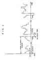
- Figure 1 depicts a typical analog sampled-data stairstep video signal which Applicant's invention is capable of receiving and synchronously sampling.
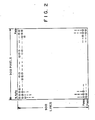
- Figure 2 shows a symmetrical visual display format that employs sequential pixels in accordance with the invention.
- Figure 3 shows a block diagram of a preferred embodiment of the invention.
- Figure 4 provides a detailed example of a controller suitable for use with the invention.
- Consider a digital video data reception and storage system designed to receive a transmitted video signal containing 900 pixels (data points) per lines and 900 lines per image field. On a symmetrical display device the system produces a square outlined image, each pixel of which comprises a small square dot having 256 different possible shades of grey from near black to near white. The horizontal retrace period for this display system consists of 40 continuous pixel clock periods. During the entire retrace period the video signal contains a negative-going horizontal sync pulse. With this system, the received video signal resembles that shown in Figure 1 (not to scale), wherein each "stairstep" analog video data line signal contains 900 separate voltage levels in 900 equally-spaced pixel clock time periods (i.e. Δt's, wherein Δt = tn - tn-1) that are applied progressing uniformly in time and space, from left to right across the display device (e.g. a cathode ray tube [CRT] screen).
- After the last line in each 900 by 900 pixel field (i.e the 900th horizontal sweep) there is a vertical sync signal that cause the system to restart a new frame at
pixel number 1 ofline number 1. In other words, after illuminating pixel X₉₀₀ Y₉₀₀ (as depicted Figure 2), the system restarts at pixel X₁, Y₁, and proceeds to reilluminate the entire display device sequentially one pixel at a time. This entire process is repeated rapidly in order to produce a visual image on the display device that has little or no flicker when viewed by the human eye. - Receiving and displaying video data as described above is well known to video system engineers. The difficulty occurs not so much in displaying the received video image as it does in capturing and storing the image data in digital form so that an entirely faithful and stable reproduction of the originally received stairstep analog video image data content may be obtained upon demand by simply interrogating a digital memory (i.e. a digital data storage device).
- The key to accomplishing proper storage of the received video image data is to sample the received video signal at or near the middle of each "stairstep" voltage level contained therein. So, for example, referring to Figure 1, the preferred time to sample the stairstep voltage level occurring between t₁ and t₂ is at t=(t₁ + t₂)/2 (in other words, at the middle of Δt). The same rule applies to each succeeding voltage level at each respective transmitting pixel clock time interval.
- What must be avoided is allowing any sampling of the received video signal to occur during the small transition time between the stairsteps, that is at or very near t₁, t₂, t₃, etc. as depicted in Figure 1. Such improper sampling would produce unreliable data since the voltage sampled would not be at either of two successive stairstep voltage levels, but rather, at some undetermined and incorrect level therebetween.
- The instant invention makes use of the fact that the number of pixel clock periods per transmitted horizontal video data line is known to be precisely 900 sequential periods equally spaced in time. Thus the pixel clock of the receiving and storing system is coerced to also have almost exactly 900 periods between the end of a received horizontal sync pulse and the start of the immediately subsequent received horizontal sync pulse.
- This is done as shown in Figure 3 by counting the number of pixel clock pulses produced by the receiving and storing system
pixel clock oscillator 301 during the received video data period (i.e. [t₉₀₀ - t₀] in Figure 1) with preset counter 302. If the count is more or less than 900 per line, the borrowoutput line 303 of the counter will so indicate (i.e. it will remain at 0 volts if the count is less than 900 per line and rise to +5 volts if the count is greater than 900 per line). This signal is then fed into thecontroller 304 which produces a small correcting change in its DC voltage output level that is fed concurrently vialine 310 directly into the control input of the receiving and storing systempixel clock oscillator 301. This oscillator is a simple pulse generator that is DC voltage controllable over a range of 2 MHz to 40 MHz corresponding to a DC input range of OV to 3V. The design of such oscillators is well known to those of ordinary skill in the electronics arts. - Sync stripper 305 includes a standard device for detecting the sync signals from a composite video signal. The one used by Applicant is the National Semiconductor Co. Model No. LM 1881.
- The output of sync stripper 305 on horizontal
sync output line 308 is used to enable the receiving and storingpixel clock oscillator 301 only during each received video line. One preferred embodiment of the invention cludes a simple adjustablepulse delay network 315, as is well known to those skilled in the electronics arts, which provides the ability to shift the sample timing points in the direction of the center of the stairstep periods of the received video signal. As a premise for the proper operation of the instant invention, it is assumed that the pixel frequency of the source video signal is approximately known (i.e., within about 10%). This is normally the case, so initial adjustment of the receiver sampling rate and phase can be accomplished rapidly. As an aid to performing the initial adjustments, it should be understood that a perfectly sampled text image will produce only two signal levels, while an aliased text image will produce intermediate signals. If the sampling frequency is more than the equivalent of 2 pixels/line in error, the sample signal will display a nodal pattern on the receiver monitor screen with the number of nodes equalling the frequency error. However, the number of sampled signal maxima or minima is relatively independent of the error except at an error of 2 or 1 pixels/line, where the number of either maxima or minima will change significantly. Monitoring the overflow signal of the A/D converter with a Dc voltmeter will provide an indication of the number of times the input signal exceeds the range of the A/D converter. When the input signal is aliased, there are fewer than the maximum overflow events, so the voltmeter reads relatively lower. As the sampling frequency approaches the source generator rate, signficantly more plentiful overflow events will occur, thus raising the measured voltage. When the frequency is within one pixel/line, the sampling frequency is correct, but the phase of the sampling clock may be in error. Adjusting the PHASE control to maximize the DC voltmeter reading will assure that all text pixels are being sampled at their correct signal value. - The output on
vertical sync outputline 309 of sync stripper 305 is used to triggercontroller 304 which in turn resets itself after each video field, reloads the preset counter 302 and applies a compensating DC control voltage alongline 310 to the receiving and storingpixel clock oscillator 301. - A more complete understanding of the mechanism of operation of
controller 304 may be discerned by reference to Figure 4. As shown, D flip-flop 401 is triggered vialine 303 by the borrow output of preset counter 302. The output of D flip-flop 401 is transferred from its inverting output terminal alongline 402 toelectronic switch 403. Whenswitch 403 is closed, its output alongline 405 toresistor 404 andcapacitor 406 is either 0 volts or +5 volts, depending on the state of D-flip-flop 401 output online 402. When the counter borrow output remains 0 volts (indicating a low count, i.e., less than 900 per line) the inverted output offlip flop 401 is +5 volts, and the charge oncapacitor 406 is raised slightly, causing a corresponding voltage increase across it; when the counter borrow output rises to +5 volts (indicating a high count, i.e., more than 900 per line) the inverted output of flip-flop 401 is 0 volts, and the charge oncapacitor 406 is lowered slightly, causing a corresponding voltage drop across it. The voltage acrosscapacitor 406 is in turn transferred vianon-inverting buffer amplifier 407 toline 310, thus automatically controlling the frequency of receiving and storingpixel clock oscillator 301. In the preferred embodiment, the sequential voltage outputs ofswitch 403 indicate the state of the accumulated count of 16 lines of pixel clock pulses within each video field (16 x 900 = 14,400 counts)Switch 403 is enabled only briefly after each video field via one-shot 408 which is triggered via syncstripper output line 309. The second one-shot 409 is used to reset D flip-flop 401 via line 410 as well as to reset preset counter 302 vialine 311 after each video field. - The gain of this "bang-bang" feedback system can be adjusted simply by adjusting the length of operation of
oneshot 408, thus accomplishing the desired precision for the number of pixel clock periods generated by receiving and storingpixel clock oscillator 301 per received video signal period. Typically, a correction of ± 0.1 pixel period/field is effected. - Using the system described above, the receiving pixel clock oscillator can be caused to stay well within the range of 899.9 to 900.1 pixel clock periods per received video image field. This accuracy assures accurate sampling of each and every received stairstep voltage level well into its respective flat region. As a result, the received analog video signal data is accurately and reliably converted by A/
D converter 306 into corresponding digital data that is stored in digital memory 307 for any desired future use. - The instant invention has been installed by Applicant into a high resolution medical imaging system with excellent results. The resulting images obtained from the digital memory are entirely without blemishes that would otherwise be present due to aliasing or other inadequate sampling methods.
- While the invention has been explained and described with reference to preferred embodiments thereof, numerous possible modifications thereto will be readily apparent to those skilled in the art without departing from the spirit and scope of the invention as recited in the claims that follow.
Claims (13)
means for detecting said received signals;
controllable variable frequency oscillator means, enabled by said detecting means during said sampled data portions of said received signals, for utilization as the sampling system clock;
digital sampling means, responsive to an output of said controllable variable frequency oscillator means, for sequentially sampling said sampled data portions of said received signals;
preset counter means, responsive to an output of said controllable variable frequency oscillator means, for counting the number of points of oscillation of said oscillator occuring between sequential synchronizing portions of said received signals; and,
control means, responsive to outputs of said preset counter means and said detecting means, for generating a compensating control signal that automatically adjusts the frequency of said variable frequency oscillator so that the number of periods of oscillation of said controllable varible frequency oscillator means occurring during said sampled data portions of said received signals substantially corresponds to a preset count.
detecting said synchronizing portions;
counting the number of periods of oscillation of a controllable receiver pixel clock oscillator occurring between successive occurrences of said synchronizing portions;
comparing said number of periods with a predetermined count;
generating a control signal that causes said oscillator to conform said number of periods with said predetermined count;
triggering an analog-to-digital converter with the output of said pixel clock oscillator during said data portions of said received analog sampled-data signal so that said analog-to-digital converter accurately digitally samples the data portions of said received analog sampled-data signals.
Applications Claiming Priority (2)
| Application Number | Priority Date | Filing Date | Title |
|---|---|---|---|
| US07/251,961 US4905085A (en) | 1988-09-29 | 1988-09-29 | Synchronous sampling system |
| US251961 | 1988-09-29 |
Publications (3)
| Publication Number | Publication Date |
|---|---|
| EP0361947A2 true EP0361947A2 (en) | 1990-04-04 |
| EP0361947A3 EP0361947A3 (en) | 1991-05-02 |
| EP0361947B1 EP0361947B1 (en) | 1994-11-30 |
Family
ID=22954097
Family Applications (1)
| Application Number | Title | Priority Date | Filing Date |
|---|---|---|---|
| EP89309952A Expired - Lifetime EP0361947B1 (en) | 1988-09-29 | 1989-09-29 | Synchronous sampling system |
Country Status (4)
| Country | Link |
|---|---|
| US (1) | US4905085A (en) |
| EP (1) | EP0361947B1 (en) |
| JP (1) | JP2574038B2 (en) |
| DE (1) | DE68919626T2 (en) |
Cited By (1)
| Publication number | Priority date | Publication date | Assignee | Title |
|---|---|---|---|---|
| WO1995001047A2 (en) * | 1993-06-10 | 1995-01-05 | Barco | A method and a device for converting a picture |
Families Citing this family (16)
| Publication number | Priority date | Publication date | Assignee | Title |
|---|---|---|---|---|
| JPH05308599A (en) * | 1991-12-30 | 1993-11-19 | Samsung Electron Co Ltd | Printing method and printing device suitable for the method |
| US5551016A (en) * | 1993-07-01 | 1996-08-27 | Queen's University At Kingston | Monitoring system and interface apparatus therefor |
| JP3149124B2 (en) * | 1995-03-06 | 2001-03-26 | 株式会社コンテック | Color signal sampling method |
| US5786868A (en) * | 1995-12-22 | 1998-07-28 | Cirrus Logic, Inc. | Automatic step generator for self-correction of sampling |
| JPH09231691A (en) * | 1996-02-27 | 1997-09-05 | Hewlett Packard Japan Ltd | Measuring device for storage device |
| JP3358432B2 (en) * | 1996-02-29 | 2002-12-16 | ソニー株式会社 | Clock signal generating apparatus and method |
| US5767916A (en) * | 1996-03-13 | 1998-06-16 | In Focus Systems, Inc. | Method and apparatus for automatic pixel clock phase and frequency correction in analog to digital video signal conversion |
| US5805233A (en) * | 1996-03-13 | 1998-09-08 | In Focus Systems, Inc. | Method and apparatus for automatic pixel clock phase and frequency correction in analog to digital video signal conversion |
| US6965400B1 (en) * | 1997-02-07 | 2005-11-15 | Canon Kabushiki Kaisha | Video input apparatus and image pickup system including the apparatus |
| US6633288B2 (en) * | 1999-09-15 | 2003-10-14 | Sage, Inc. | Pixel clock PLL frequency and phase optimization in sampling of video signals for high quality image display |
| US6636205B1 (en) | 2000-04-10 | 2003-10-21 | Infocus Corporation | Method and apparatus for determining a clock tracking frequency in a single vertical sync period |
| TW558712B (en) * | 2001-01-05 | 2003-10-21 | Benq Corp | Method for automatically adjusting display quality |
| JP2011154060A (en) * | 2010-01-26 | 2011-08-11 | Canon Inc | Display device |
| CN112446235A (en) * | 2019-08-28 | 2021-03-05 | 广东博智林机器人有限公司 | PSD-based signal peak-to-peak value acquisition device and method and light spot gravity center detection method |
| CN114035474A (en) * | 2021-11-10 | 2022-02-11 | 中国科学院微电子研究所 | Sampling signal synchronous control system |
| CN115037840B (en) * | 2022-04-29 | 2023-02-28 | 北京航空航天大学 | Data synchronization method and device of scanning and imaging combined system and scanning and imaging combined system |
Citations (5)
| Publication number | Priority date | Publication date | Assignee | Title |
|---|---|---|---|---|
| US3971063A (en) * | 1974-03-16 | 1976-07-20 | Quantel Limited | Digital time base corrector oscillators |
| US4065787A (en) * | 1976-01-28 | 1977-12-27 | Quantel Limited | Time base corrector |
| WO1985005744A1 (en) * | 1984-06-06 | 1985-12-19 | Motorola, Inc. | Frequency controlled oscillator |
| US4613827A (en) * | 1984-07-28 | 1986-09-23 | Sony Corporation | Write clock pulse generator used for a time base corrector |
| EP0218402A2 (en) * | 1985-10-01 | 1987-04-15 | Seiko Instruments Inc. | A sampling clock phase correction circuit |
Family Cites Families (12)
| Publication number | Priority date | Publication date | Assignee | Title |
|---|---|---|---|---|
| US3259851A (en) * | 1961-11-01 | 1966-07-05 | Avco Corp | Digital system for stabilizing the operation of a variable frequency oscillator |
| US3287655A (en) * | 1964-11-30 | 1966-11-22 | Douglas A Venn | Digital control for disciplining oscillators |
| US3978519A (en) * | 1974-03-16 | 1976-08-31 | Quantel Limited | Digital time base correctors for television equipment |
| US4074307A (en) * | 1975-08-14 | 1978-02-14 | Rca Corporation | Signal processor using charge-coupled devices |
| US4105946A (en) * | 1977-07-06 | 1978-08-08 | Sansui Electric Co., Ltd. | Frequency synthesizer with phase locked loop and counter |
| US4253116A (en) * | 1979-11-27 | 1981-02-24 | Rca Corporation | Television synchronizing system operable from nonstandard signals |
| EP0079971B1 (en) * | 1981-11-19 | 1985-07-17 | Deutsche ITT Industries GmbH | Digital circuit delivering a binary signal whenever the frequency ration of the line/and the field frequency occurs |
| JPS58191573A (en) * | 1982-05-06 | 1983-11-08 | Victor Co Of Japan Ltd | Horizontal scanning frequency multiplier circuit |
| JPS60160220A (en) * | 1984-01-31 | 1985-08-21 | Fujitsu Ltd | Drift detecting circuit |
| US4528521A (en) * | 1984-02-09 | 1985-07-09 | At&T Information Systems Inc. | Precision control frequency synthesizer having an unstable, variable frequency input signal |
| JPS6153817A (en) * | 1984-08-23 | 1986-03-17 | Nec Corp | Timing generating device |
| JPS62172875A (en) * | 1986-01-27 | 1987-07-29 | Nippon Hoso Kyokai <Nhk> | Reproducing system for multiplex sample transmission signal |
-
1988
- 1988-09-29 US US07/251,961 patent/US4905085A/en not_active Expired - Lifetime
-
1989
- 1989-09-29 EP EP89309952A patent/EP0361947B1/en not_active Expired - Lifetime
- 1989-09-29 JP JP1252476A patent/JP2574038B2/en not_active Expired - Fee Related
- 1989-09-29 DE DE68919626T patent/DE68919626T2/en not_active Expired - Fee Related
Patent Citations (5)
| Publication number | Priority date | Publication date | Assignee | Title |
|---|---|---|---|---|
| US3971063A (en) * | 1974-03-16 | 1976-07-20 | Quantel Limited | Digital time base corrector oscillators |
| US4065787A (en) * | 1976-01-28 | 1977-12-27 | Quantel Limited | Time base corrector |
| WO1985005744A1 (en) * | 1984-06-06 | 1985-12-19 | Motorola, Inc. | Frequency controlled oscillator |
| US4613827A (en) * | 1984-07-28 | 1986-09-23 | Sony Corporation | Write clock pulse generator used for a time base corrector |
| EP0218402A2 (en) * | 1985-10-01 | 1987-04-15 | Seiko Instruments Inc. | A sampling clock phase correction circuit |
Cited By (3)
| Publication number | Priority date | Publication date | Assignee | Title |
|---|---|---|---|---|
| WO1995001047A2 (en) * | 1993-06-10 | 1995-01-05 | Barco | A method and a device for converting a picture |
| WO1995001047A3 (en) * | 1993-06-10 | 1995-03-02 | Barco | A method and a device for converting a picture |
| US5801780A (en) * | 1993-06-10 | 1998-09-01 | Barco | Method and a device for converting a picture |
Also Published As
| Publication number | Publication date |
|---|---|
| DE68919626T2 (en) | 1995-06-01 |
| US4905085A (en) | 1990-02-27 |
| EP0361947B1 (en) | 1994-11-30 |
| EP0361947A3 (en) | 1991-05-02 |
| JPH02170689A (en) | 1990-07-02 |
| JP2574038B2 (en) | 1997-01-22 |
| DE68919626D1 (en) | 1995-01-12 |
Similar Documents
| Publication | Publication Date | Title |
|---|---|---|
| US4905085A (en) | Synchronous sampling system | |
| JP3220023B2 (en) | Liquid crystal display | |
| US3984624A (en) | Video system for conveying digital and analog information | |
| US5579348A (en) | Method and apparatus for improving the apparent accuracy of a data receiver clock circuit | |
| US4400717A (en) | Color slow-scan TV system and method | |
| EP0473338A2 (en) | Bit synchronization with elastic memory | |
| JPH06188870A (en) | Clock regenerator | |
| US5767917A (en) | Method and apparatus for multi-standard digital television synchronization | |
| EP0360519B1 (en) | Timing measurement for jitter display | |
| EP0249281A1 (en) | Television picture display device | |
| EP0138164A2 (en) | Method and apparatus for sampling and processing a video signal | |
| EP0378875B1 (en) | Noise measurement for video signals | |
| EP0090426A2 (en) | Method and apparatus for measuring horizontal sync subcarrier phase | |
| US4713691A (en) | Interface circuit of video signal hard copy apparatus | |
| US3863022A (en) | Television signal clocked delay line for delay by an integer number of horizontal scanning lines driven by a pilot signal | |
| US5068717A (en) | Method and apparatus for synchronization in a digital composite video system | |
| US4126886A (en) | Jitter correcting system using a pseudo composite video signal for use in a video reproduction apparatus | |
| US4874992A (en) | Closed loop adaptive raster deflection signal generator | |
| KR100466553B1 (en) | A delay correction circuit | |
| CA1099403A (en) | Vertical synchronizing signal detector for television video signal reception | |
| US3991270A (en) | Circuit arrangement for line synchronization in a television receiver | |
| EP0217091A1 (en) | Velocity error correcting circuit for time base error corrector | |
| US5061904A (en) | Phase locked loop having sampling gate phase detector | |
| FR2571162A1 (en) | BASIC TIME CIRCUIT FOR VARIING THE HORIZONTAL FORMAT OF A FRAME SCANNING SCREEN. | |
| EP1205065A1 (en) | Method and apparatus for providing a clock signal with high frequency accuracy |
Legal Events
| Date | Code | Title | Description |
|---|---|---|---|
| PUAI | Public reference made under article 153(3) epc to a published international application that has entered the european phase |
Free format text: ORIGINAL CODE: 0009012 |
|
| AK | Designated contracting states |
Kind code of ref document: A2 Designated state(s): BE DE ES FR GB IT NL SE |
|
| PUAL | Search report despatched |
Free format text: ORIGINAL CODE: 0009013 |
|
| AK | Designated contracting states |
Kind code of ref document: A3 Designated state(s): BE DE ES FR GB IT NL SE |
|
| 17P | Request for examination filed |
Effective date: 19910515 |
|
| 17Q | First examination report despatched |
Effective date: 19930518 |
|
| GRAA | (expected) grant |
Free format text: ORIGINAL CODE: 0009210 |
|
| AK | Designated contracting states |
Kind code of ref document: B1 Designated state(s): BE DE ES FR GB IT NL SE |
|
| PG25 | Lapsed in a contracting state [announced via postgrant information from national office to epo] |
Ref country code: IT Free format text: LAPSE BECAUSE OF FAILURE TO SUBMIT A TRANSLATION OF THE DESCRIPTION OR TO PAY THE FEE WITHIN THE PRESCRIBED TIME-LIMIT;WARNING: LAPSES OF ITALIAN PATENTS WITH EFFECTIVE DATE BEFORE 2007 MAY HAVE OCCURRED AT ANY TIME BEFORE 2007. THE CORRECT EFFECTIVE DATE MAY BE DIFFERENT FROM THE ONE RECORDED. Effective date: 19941130 Ref country code: ES Free format text: THE PATENT HAS BEEN ANNULLED BY A DECISION OF A NATIONAL AUTHORITY Effective date: 19941130 Ref country code: BE Effective date: 19941130 Ref country code: NL Effective date: 19941130 |
|
| REF | Corresponds to: |
Ref document number: 68919626 Country of ref document: DE Date of ref document: 19950112 |
|
| ET | Fr: translation filed | ||
| PG25 | Lapsed in a contracting state [announced via postgrant information from national office to epo] |
Ref country code: SE Effective date: 19950228 |
|
| NLV1 | Nl: lapsed or annulled due to failure to fulfill the requirements of art. 29p and 29m of the patents act | ||
| PLBE | No opposition filed within time limit |
Free format text: ORIGINAL CODE: 0009261 |
|
| STAA | Information on the status of an ep patent application or granted ep patent |
Free format text: STATUS: NO OPPOSITION FILED WITHIN TIME LIMIT |
|
| 26N | No opposition filed | ||
| REG | Reference to a national code |
Ref country code: GB Ref legal event code: 732E |
|
| REG | Reference to a national code |
Ref country code: FR Ref legal event code: TP |
|
| PGFP | Annual fee paid to national office [announced via postgrant information from national office to epo] |
Ref country code: FR Payment date: 19990909 Year of fee payment: 11 |
|
| PGFP | Annual fee paid to national office [announced via postgrant information from national office to epo] |
Ref country code: GB Payment date: 19990929 Year of fee payment: 11 |
|
| PGFP | Annual fee paid to national office [announced via postgrant information from national office to epo] |
Ref country code: DE Payment date: 19991001 Year of fee payment: 11 |
|
| PG25 | Lapsed in a contracting state [announced via postgrant information from national office to epo] |
Ref country code: GB Free format text: LAPSE BECAUSE OF NON-PAYMENT OF DUE FEES Effective date: 20000929 |
|
| REG | Reference to a national code |
Ref country code: GB Ref legal event code: 732E |
|
| GBPC | Gb: european patent ceased through non-payment of renewal fee |
Effective date: 20000929 |
|
| PG25 | Lapsed in a contracting state [announced via postgrant information from national office to epo] |
Ref country code: FR Free format text: LAPSE BECAUSE OF NON-PAYMENT OF DUE FEES Effective date: 20010531 |
|
| PG25 | Lapsed in a contracting state [announced via postgrant information from national office to epo] |
Ref country code: DE Free format text: LAPSE BECAUSE OF NON-PAYMENT OF DUE FEES Effective date: 20010601 |
|
| REG | Reference to a national code |
Ref country code: FR Ref legal event code: ST |
|
| REG | Reference to a national code |
Ref country code: FR Ref legal event code: TP |