EP0356622A2 - Method and device for positioning a welding laser - Google Patents
Method and device for positioning a welding laser Download PDFInfo
- Publication number
- EP0356622A2 EP0356622A2 EP89109568A EP89109568A EP0356622A2 EP 0356622 A2 EP0356622 A2 EP 0356622A2 EP 89109568 A EP89109568 A EP 89109568A EP 89109568 A EP89109568 A EP 89109568A EP 0356622 A2 EP0356622 A2 EP 0356622A2
- Authority
- EP
- European Patent Office
- Prior art keywords
- soldering
- laser
- positioning
- detector
- scanner
- Prior art date
- Legal status (The legal status is an assumption and is not a legal conclusion. Google has not performed a legal analysis and makes no representation as to the accuracy of the status listed.)
- Withdrawn
Links
Images


Classifications
-
- B—PERFORMING OPERATIONS; TRANSPORTING
- B23—MACHINE TOOLS; METAL-WORKING NOT OTHERWISE PROVIDED FOR
- B23K—SOLDERING OR UNSOLDERING; WELDING; CLADDING OR PLATING BY SOLDERING OR WELDING; CUTTING BY APPLYING HEAT LOCALLY, e.g. FLAME CUTTING; WORKING BY LASER BEAM
- B23K26/00—Working by laser beam, e.g. welding, cutting or boring
- B23K26/02—Positioning or observing the workpiece, e.g. with respect to the point of impact; Aligning, aiming or focusing the laser beam
- B23K26/04—Automatically aligning, aiming or focusing the laser beam, e.g. using the back-scattered light
-
- G—PHYSICS
- G05—CONTROLLING; REGULATING
- G05B—CONTROL OR REGULATING SYSTEMS IN GENERAL; FUNCTIONAL ELEMENTS OF SUCH SYSTEMS; MONITORING OR TESTING ARRANGEMENTS FOR SUCH SYSTEMS OR ELEMENTS
- G05B19/00—Programme-control systems
- G05B19/02—Programme-control systems electric
- G05B19/18—Numerical control [NC], i.e. automatically operating machines, in particular machine tools, e.g. in a manufacturing environment, so as to execute positioning, movement or co-ordinated operations by means of programme data in numerical form
- G05B19/19—Numerical control [NC], i.e. automatically operating machines, in particular machine tools, e.g. in a manufacturing environment, so as to execute positioning, movement or co-ordinated operations by means of programme data in numerical form characterised by positioning or contouring control systems, e.g. to control position from one programmed point to another or to control movement along a programmed continuous path
- G05B19/39—Numerical control [NC], i.e. automatically operating machines, in particular machine tools, e.g. in a manufacturing environment, so as to execute positioning, movement or co-ordinated operations by means of programme data in numerical form characterised by positioning or contouring control systems, e.g. to control position from one programmed point to another or to control movement along a programmed continuous path using a combination of the means covered by at least two of the preceding sub-groups G05B19/21, G05B19/27, and G05B19/33
Definitions
- the invention relates to a method and a device for carrying out this method for positioning soldering lasers according to the preamble of claim 1.
- the invention has for its object to provide a method and a device of the type mentioned, which both simplifies the positioning and its accuracy below the series tolerances and an exact, individual position adjustment within an automatic function sequence is quickly guaranteed.
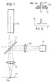
- the method for positioning is outlined in FIG. 1.
- a beam splitter 11 Arranged in the beam path of a laser 10 is a beam splitter 11, which directs one half of the beam part via focusing optics 12 to the contact 13a to be soldered on chip carrier 13 and the other half beam part via focusing optics 12a to a detector 14, which is precise and unambiguous the reflective pin contacts, circuitry and components registered on the chip carrier.
- a detector 14 which is precise and unambiguous the reflective pin contacts, circuitry and components registered on the chip carrier.
- the electrical signals generated by the detector (s) 14 - preferably the aforementioned photodiodes 16 - are now used to adjust the positioning, ie the robot, XY table and preferably the scanner are stopped, the soldering laser is switched on and the soldering process is initiated.
- the positioning device only continues to run when the soldering laser is switched off.
- the reflection method can work without local coordinates and the entire circuit can be scanned.
- Laser scanning is particularly suitable for this. It has been shown that the usual rough positioning can be retained and only the individual fine adjustment in the tenth to thousandth range is to be carried out.
- FIG. 3a it is proposed, as sketched in FIG. 3a, to arrange four photodiodes 16 like a cloverleaf in order to arrange the optics of the laser 10 and to connect them via a compensation circuit - as is known to the person skilled in the art.
- the stop signal for the positioning and the start signal for the soldering laser are only triggered after the adjustment has been carried out.
- an IR detector is assigned to the soldering laser for temperature control, as has already been suggested, for example, from the document referred to in the prior art.
- the additional coupling of an IR detector 17 via IR optical waveguides makes it possible to substantially reduce the cost of the relatively complex laser soldering devices, as the explanations below explain.
- the proposed method produces optimal results, in particular in the case of series soldering of chip carriers and rows of pins in a simple geometric arrangement.
- these cables are assigned to one soldering laser 10 via beam splitters.
- the IR detector 17 now works frequently with a very short response time in the range of 1 ms, so that it is considerably less than the laser soldering time of greater than 50 ms, several different laser soldering points can be monitored without problems via several IR optical fibers and the different temperature / Time curves can also be recorded by a single IR detector 17.
- a method and a device for fine positioning of soldering lasers is now created, which uses a positioning device - preferably a scanner - to scan the substrate to be soldered with a laser beam and to track the reflected light intensity with a light detector - photodiode.
- a strong reflection signal occurs at the shiny metallic, mostly pre-tinned solder points, which is used for fine positioning, stopping and switching on the soldering laser.
Landscapes
- Engineering & Computer Science (AREA)
- Physics & Mathematics (AREA)
- Optics & Photonics (AREA)
- Human Computer Interaction (AREA)
- Manufacturing & Machinery (AREA)
- General Physics & Mathematics (AREA)
- Automation & Control Theory (AREA)
- Plasma & Fusion (AREA)
- Mechanical Engineering (AREA)
- Laser Beam Processing (AREA)
- Length Measuring Devices By Optical Means (AREA)
Abstract
Description
Die Erfindung bezieht sich auf ein Verfahren und eine Einrichtung zur Durchführung dieses Verfahrens zur Positionierung von Lötlasern gemäß dem Oberbegriff des Anspruchs 1.The invention relates to a method and a device for carrying out this method for positioning soldering lasers according to the preamble of claim 1.
Durch die DE-OS 36 06 764 ist es bekannt, beim Laser-Mikrolöten die Lötstellen mittels Roboter-, XY-Tisch oder Scanner-Programm anzusteuern. Hierbei ist eine Positionsgenauigkeit von ± 50 µm üblich. Sollen nun Genauigkeiten von ± 5 µm erzielt werden, so ist dies nur mit großem Aufwand und mit langen Positionierzeiten möglich. Außerdem werden dann hohe Positioniergenauigkeiten bei den Lötgeometrien - also Lage, Form und Größe - vorausgesetzt und damit unrealistisch enge oder zumindest nur sehr aufwendig erreichbare Fertigungsstreuungen und Toleranzen erforderlich. Weiterhin sind beim Stand der Technik aufwendige Bildverarbeitungseinrichtungen notwendig.From DE-OS 36 06 764 it is known to control the solder joints in laser micro soldering using a robot, XY table or scanner program. A position accuracy of ± 50 µm is usual. If accuracies of ± 5 µm are now to be achieved, this is only possible with great effort and with long positioning times. In addition, high positioning accuracies in the soldering geometries - that is, position, shape and size - are assumed and thus unrealistically narrow or at least very difficult to achieve manufacturing variations and tolerances are required. Furthermore, complex image processing devices are necessary in the prior art.
Zwischenzeitlich zeigt es sich aber, daß das Laser-Mikrolöten nicht nur voll automatisiert sein soll, sondern daß auch sehr feine Lötkontakte im Zehntel-Millimeterbereich zu erzeugen sind, wie sie beispielsweise bei Chipträgern und Mikrobauelementen für die Oberflächemontage gefordert werden. So erfordern hochpolige Chipträger mit über 300 Anschlüssen sehr enge Lötabstände und kleinere Pads und damit eine sehr hohe Positioniergenauig keit. Hierzu aber sind bei den bisherigen Positioniereinrichtungen aufwendige, zeitraubende Nachjustierungen zur Feinabgleichung erforderlich.In the meantime, however, it has been shown that laser micro soldering should not only be fully automated, but also that very fine solder contacts in the tenths of a millimeter range must be produced, as are required, for example, in chip carriers and microcomponents for surface mounting. For example, multi-pin chip carriers with over 300 connections require very narrow soldering gaps and smaller pads and thus very high positioning accuracy. However, this requires time-consuming readjustments for fine adjustment in the previous positioning devices.
Der Erfindung liegt die Aufgabe zugrunde, ein Verfahren und eine Einrichtung der eingangs genannten Art zu schaffen, womit sowohl eine Vereinfachung der Positionierung als auch deren Genauigkeit unterhalb der Serientoleranzen ermöglicht wird und eine exakte, individuelle Positionsanpassung innerhalb eines automatischen Funktionsablaufs schnell gewährleistet ist.The invention has for its object to provide a method and a device of the type mentioned, which both simplifies the positioning and its accuracy below the series tolerances and an exact, individual position adjustment within an automatic function sequence is quickly guaranteed.
Diese Aufgabe wird durch das im Anspruch 1 aufgezeigte Verfahren und die im Anspruch 3 konzipierte Einrichtung gelöst. In den Unteransprüchen sind Ausgestaltungen und Weiterbildungen von Verfahren und Einrichtung aufgezeigt und in der nachfolgenden Beschreibung ist ein Ausführungsbeispiel erläutert sowie in den Figuren der Zeichnung skizziert. Es zeigen:
- Fig. 1 ein Schemabild der Laser-Detektoranordnung,
- Fig. 1a ein Schnitt durch eine Lötstelle eines Chipträgers,
- Fig. 1b ein Diagramm des Detektorsignals an der Lötstelle gemäß Fig. 1a,
- Fig. 2 ein Diagramm der Reflexionssignale einer engeren Stiftkontaktreihe in einer bestimmten Zeit,
- Fig. 3a ein Schemabild einer Fotodiodenanordnung um die Optik des Lasers,
- Fig. 3b ein Schemabild einer Fotodiodenanordnung und eines IR-Detektors um die Optik des Lasers,
- Fig. 4 ein Blockschaltbild eines Ausführungsbeispiels einer Positioniereinrichtung.
- 1 is a schematic image of the laser detector arrangement,
- 1a shows a section through a solder joint of a chip carrier,
- 1b is a diagram of the detector signal at the solder joint according to FIG. 1a,
- 2 shows a diagram of the reflection signals of a closer row of pin contacts in a certain time,
- 3a shows a schematic image of a photodiode arrangement around the optics of the laser,
- 3b is a schematic image of a photodiode arrangement and an IR detector around the optics of the laser,
- Fig. 4 is a block diagram of an embodiment of a positioning device.
Die Methode für eine Positionierung, wie sie hier in einem Ausführungsbeispiel vorgeschlagen wird ist in der Fig. 1 skizziert. In den Strahlengang eines Lasers 10 ist ein Strahlteiler 11 angeordnet, der den einen hälftigen Strahlteil über eine Fokussieroptik 12 auf den zu lötenden Kontakt 13a auf dem Chipträger 13 richtet und den anderen hälftigen Strahlteil über die Fokussieroptik 12a auf einen Detektor 14, der exakt und eindeutig die reflektierenden Stiftkontakte, Schaltungs- und Bauelemente auf dem Chipträger registriert. Bei der Entwicklung des hier vorgeschlagenen Verfahrens wurde entdeckt, daß gewöhnliche, handelsübliche, bei 630 µm empfindliche Fotodioden, die neben oder im Strahlengang des Pilotlasers angeordnet sind, völlig einwandfrei und exakt die unbeschichteten, zumeist je doch vorverzinnten Kontaktstellen oder Anschlußstellen registrieren. Die von dem oder den Detektoren 14 - vorzugsweise die genannten Fotodioden 16 - erzeugten elektrischen Signale werden nun zur Einstellung der Positionierung benutzt, d. h. der Roboter, XY-Tisch und vorzugsweise der Scanner werden angehalten, der Lötlaser angeschaltet und der Lötvorgang initiert. Erst wenn der Lötlaser ausgeschaltet ist, läuft das Positioniergerät weiter.The method for positioning, as proposed here in an exemplary embodiment, is outlined in FIG. 1. Arranged in the beam path of a
Es hat sich gezeigt, daß vorstehendes Verfahren sich besonders für eine schnellarbeitende Scann-Einrichtung - wie sie beispielsweise im Blockschaltbild gemäß Fig. 4 skizziert ist - eignet. Hier werden die einzelnen Positionen grob angesteuert und über einen analogen Abgleich des Reflexionssignals die jeweilige Feinpositionierung über die Scannerspiegel vorgenommen. Hier können nun erstmals aufwandslos Einstellzeiten von 1 bis 2 ms erreicht werden.It has been shown that the above method is particularly suitable for a fast-working scanning device - such as that outlined in the block diagram according to FIG. 4. Here the individual positions are roughly controlled and the respective fine positioning is carried out via the scanner mirrors via an analog adjustment of the reflection signal. Here, setting times of 1 to 2 ms can now be achieved effortlessly for the first time.
Prinzipiell kann bei dem Reflexionsverfahren ohne Ortskoordinaten gearbeitet und die gesamte Schaltung abgetastet werden. Hierfür eignet sich besonders das Laser-Scanning. Es hat sich gezeigt, daß die übliche Grobpositionierung beibehalten werden kann und nur die individuelle Feinanpassung im Zehntel- bis Tausendstell-Bereich durchzuführen ist.In principle, the reflection method can work without local coordinates and the entire circuit can be scanned. Laser scanning is particularly suitable for this. It has been shown that the usual rough positioning can be retained and only the individual fine adjustment in the tenth to thousandth range is to be carried out.
In einem Ausführungsbeispiel wird nun vorgeschlagen, wie in Fig. 3a skizziert, vier Fotodioden 16 kleeblattartig um die Optik des Lasers 10 anzuordnen und über eine Kompensationsschaltung - wie sie dem Fachmann geläufig ist - zu verbinden. Das Stopsignal für die Positionierung und das Startsignal für den Lötlaser wird erst nach Vollzug des Abgleichs ausgelöst.In one exemplary embodiment, it is proposed, as sketched in FIG. 3a, to arrange four
In einem weiteren Ausführungsbeispiel. das in Fig. 3b schematisch dargestellt ist, wird dem Lötlaser zur Temperatursteuerung ein IR-Detektor zugeordnet, wie dies beispielsweise aus der zum Stand der Technik angezogenen Druckschrift schon vorgeschlagen ist. In Kombination mit den Fotodio den 16 kann durch die zusätzliche Einkopplung eines IR-Detektors 17 über IR-Lichtwellenleiter eine wesentliche Verbilligung der relativ aufwendigen Laserlötgeräte erzielt werden, wie nachstehende Ausführungen erläutern.In another embodiment. which is shown schematically in FIG. 3b, an IR detector is assigned to the soldering laser for temperature control, as has already been suggested, for example, from the document referred to in the prior art. In combination with the Fotodio 16, the additional coupling of an
Das vorgeschlagene Verfahren erbringt optimale Ergebnisse insbesondere bei Serienlötungen von Chipträgern und Stiftreihen in einfacher geometrischer Anordnung. Nun ist es möglich, nach einer Positionierung mehrere Verlötungen gleichzeitig mit mehreren Lichtwellenleiterkabeln vorzunehmen. Hierzu sind diese Kabel über Strahlteiler dem einen Lötlaser 10 zugeordnet. Da nun der IR-Detektor 17 frequentiell mit einer sehr kurzen - Ansprechzeit im Bereich von 1ms - arbeitet, damit also erheblich unter der Laserlötzeit von größer als 50 ms liegt, können problemlos mehrere verschiedene Laserlötstellen über mehrere IR-Lichtwellenleiter überwacht und die verschiedenen Temperatur-/Zeitkurven auch von einem einzigen IR-Detektor 17 aufgenommen werden.The proposed method produces optimal results, in particular in the case of series soldering of chip carriers and rows of pins in a simple geometric arrangement. Now it is possible, after positioning, to carry out several solderings simultaneously with several fiber optic cables. For this purpose, these cables are assigned to one soldering
Damit ist nun ein Verfahren und eine Einrichtung zur Feinpositionierung von Lötlasern geschaffen, das mittels einer Positioniereinrichtung - vorzugsweise ein Scanner - das zu verlötende Substrat mit einem Laserstrahl abtastet und mit einem Lichtdetektor - Fotodiode - die reflektierte Lichtintensität verfolgt. An den metallisch glänzenden, meist vorverzinnten Lötstellen tritt ein starkes Reflexionssignal auf, das zum Feinpositionieren, Anhalten und Aufschalten des Lötlasers verwendet wird.A method and a device for fine positioning of soldering lasers is now created, which uses a positioning device - preferably a scanner - to scan the substrate to be soldered with a laser beam and to track the reflected light intensity with a light detector - photodiode. A strong reflection signal occurs at the shiny metallic, mostly pre-tinned solder points, which is used for fine positioning, stopping and switching on the soldering laser.
Das in Figur 4 gezeigte Blockschaltbild dürfte im Zusammenhang mit vorstehenden Ausführungen so deutlich und verständlich sein, daß weitere Ausführungen hierzu nicht mehr erforderlich erscheinen.The block diagram shown in FIG. 4 should be so clear and understandable in connection with the above statements that further explanations no longer appear to be necessary.
Claims (6)
Applications Claiming Priority (2)
| Application Number | Priority Date | Filing Date | Title |
|---|---|---|---|
| DE3829350A DE3829350A1 (en) | 1988-08-30 | 1988-08-30 | METHOD AND DEVICE FOR POSITIONING LOETLASERS |
| DE3829350 | 1988-08-30 |
Publications (2)
| Publication Number | Publication Date |
|---|---|
| EP0356622A2 true EP0356622A2 (en) | 1990-03-07 |
| EP0356622A3 EP0356622A3 (en) | 1992-10-14 |
Family
ID=6361863
Family Applications (1)
| Application Number | Title | Priority Date | Filing Date |
|---|---|---|---|
| EP19890109568 Withdrawn EP0356622A3 (en) | 1988-08-30 | 1989-05-26 | Method and device for positioning a welding laser |
Country Status (2)
| Country | Link |
|---|---|
| EP (1) | EP0356622A3 (en) |
| DE (1) | DE3829350A1 (en) |
Cited By (1)
| Publication number | Priority date | Publication date | Assignee | Title |
|---|---|---|---|---|
| CN114355503A (en) * | 2020-10-13 | 2022-04-15 | 飞巽传感技术(上海)有限公司 | Manufacturing method and system of optical fiber sensor |
Families Citing this family (4)
| Publication number | Priority date | Publication date | Assignee | Title |
|---|---|---|---|---|
| EP0597524B1 (en) * | 1992-11-09 | 1997-08-06 | Koninklijke Philips Electronics N.V. | Method and device for investigating an object by means of a reflectable radiation beam |
| DE19850595C2 (en) | 1998-11-03 | 2002-07-04 | Hahn Schickard Ges | Process for laser soldering semiconductor chips |
| DE10047056A1 (en) * | 2000-09-22 | 2002-04-11 | Volkswagen Ag | Device for laser welding has a curved wire feeding line running through a region which lies before a seam determining sensor and below the sensor through to the seam site without crossing the sensor beam |
| DE10126725A1 (en) * | 2001-05-31 | 2002-12-05 | Volkswagen Ag | Laser machining of workpieces, e.g. for vehicle body parts, involves detecting light from positioning laser reflected at workpiece and deriving position of machining laser or laser head from it |
Citations (4)
| Publication number | Priority date | Publication date | Assignee | Title |
|---|---|---|---|---|
| US3485996A (en) * | 1967-01-11 | 1969-12-23 | Ibm | Laser welding |
| FR2352624A1 (en) * | 1976-05-28 | 1977-12-23 | Siemens Ag | PROCESS FOR PERFORMING THE PRECISE MACHINING OF A WORKPIECE, PLACED IN THE WORKPLAN OF A MACHINING LASER, AND DEVICE FOR IMPLEMENTING THIS PROCESS |
| US4125755A (en) * | 1977-06-23 | 1978-11-14 | Western Electric Co., Inc. | Laser welding |
| US4663513A (en) * | 1985-11-26 | 1987-05-05 | Spectra-Physics, Inc. | Method and apparatus for monitoring laser processes |
Family Cites Families (7)
| Publication number | Priority date | Publication date | Assignee | Title |
|---|---|---|---|---|
| US4481418A (en) * | 1982-09-30 | 1984-11-06 | Vanzetti Systems, Inc. | Fiber optic scanning system for laser/thermal inspection |
| FR2559695B1 (en) * | 1984-02-20 | 1995-04-21 | Mitsubishi Electric Corp | METHOD AND APPARATUS FOR DETECTING AND CONTROLLING THE POSITION OF AN ELECTRONIC WELDING BEAM |
| FR2587513B1 (en) * | 1985-09-16 | 1987-10-30 | Commissariat Energie Atomique | DEVICE FOR REAL-TIME MONITORING OF A TOTAL PENETRATION WELDING, SUITABLE FOR A JOINT INACCESSIBLE TO DIRECT OBSERVATION |
| DE3539933A1 (en) * | 1985-11-11 | 1987-05-14 | Nixdorf Computer Ag | DEVICE FOR SOLELING ELECTRONIC COMPONENTS ON A CIRCUIT BOARD |
| DE3543681A1 (en) * | 1985-12-11 | 1987-06-19 | Jurca Marius Christian | Device for producing a weld |
| DE3606764A1 (en) * | 1986-03-01 | 1987-09-03 | Messerschmitt Boelkow Blohm | METHOD AND DEVICE FOR MICROLOETING |
| DE3626944A1 (en) * | 1986-08-08 | 1988-02-18 | Bias Forschung & Entwicklung | Method and apparatus for focussing and controlling a high-output energy source |
-
1988
- 1988-08-30 DE DE3829350A patent/DE3829350A1/en active Granted
-
1989
- 1989-05-26 EP EP19890109568 patent/EP0356622A3/en not_active Withdrawn
Patent Citations (4)
| Publication number | Priority date | Publication date | Assignee | Title |
|---|---|---|---|---|
| US3485996A (en) * | 1967-01-11 | 1969-12-23 | Ibm | Laser welding |
| FR2352624A1 (en) * | 1976-05-28 | 1977-12-23 | Siemens Ag | PROCESS FOR PERFORMING THE PRECISE MACHINING OF A WORKPIECE, PLACED IN THE WORKPLAN OF A MACHINING LASER, AND DEVICE FOR IMPLEMENTING THIS PROCESS |
| US4125755A (en) * | 1977-06-23 | 1978-11-14 | Western Electric Co., Inc. | Laser welding |
| US4663513A (en) * | 1985-11-26 | 1987-05-05 | Spectra-Physics, Inc. | Method and apparatus for monitoring laser processes |
Cited By (1)
| Publication number | Priority date | Publication date | Assignee | Title |
|---|---|---|---|---|
| CN114355503A (en) * | 2020-10-13 | 2022-04-15 | 飞巽传感技术(上海)有限公司 | Manufacturing method and system of optical fiber sensor |
Also Published As
| Publication number | Publication date |
|---|---|
| EP0356622A3 (en) | 1992-10-14 |
| DE3829350C2 (en) | 1991-07-18 |
| DE3829350A1 (en) | 1990-03-01 |
Similar Documents
| Publication | Publication Date | Title |
|---|---|---|
| DE60019573T2 (en) | LASER CALIBRATION DEVICE AND METHOD | |
| DE69632371T2 (en) | Method for aligning optical axes, device therefor, inspection method for optical devices, inspection device, production method for optical modules and device for producing an optical module | |
| DE10105943B4 (en) | Fiber optic lens system for coupling fibers with surface mounted devices | |
| DE19819164C1 (en) | Optical data communication module | |
| EP2073047B1 (en) | An assembly and alignment method for an electro-optical device and a measuring device assembled and aligned according to the method | |
| WO2019029765A9 (en) | Position-tolerance-insensitive contacting module for contacting optoelectronic chips | |
| EP0660467A1 (en) | Optoelectronical element and method of making the same | |
| DE19844701C1 (en) | Method for adjusting an optoelectronic component and component | |
| DE4008605A1 (en) | MULTIPLEXER FOR A CONTINUOUS, HIGH-PERFORMANCE LASER | |
| EP0223066B1 (en) | Device for soldering electronic components on a printed-circuit board | |
| EP0779526A2 (en) | Optical and/or electrooptical connection and process for its fabrication | |
| DE4235549A1 (en) | Light source unit, e.g. for laser printer or copier - contains multiple light emitting semiconductor laser chips arranged in mounting device to emit parallel light beams through collimator lens | |
| DE102020100217A1 (en) | Method for automated beam positioning of a laser beam with respect to a nozzle of a laser processing head and laser processing system for processing a workpiece with a laser beam | |
| DE4209524A1 (en) | Method for position detection and / or division check and / or coplanarity check of the connections of components and placement head for the automatic placement of components | |
| EP0356622A2 (en) | Method and device for positioning a welding laser | |
| DE3307669C2 (en) | ||
| EP0380179A1 (en) | Method and device for the alignment of an optical fiber relative to a lens of a plug connector | |
| DE10163726A1 (en) | Alignment of optical arrangements | |
| EP0800756B1 (en) | Device for determining the position of connections of components | |
| DE10213577B3 (en) | Process for simultaneous laser beam soldering | |
| EP0942302A2 (en) | Electrooptical module | |
| DE19704502C1 (en) | Laser module with fine adjustment method e.g. for micrometre range transmission engineering | |
| DE10307763B4 (en) | Electro-optical module for transmitting and / or receiving optical signals of at least two optical data channels | |
| EP0783715B1 (en) | Optical coupling arrangement | |
| DE4002370B4 (en) | Method and device for adjusting the optical coupling of optical waveguides and optical components |
Legal Events
| Date | Code | Title | Description |
|---|---|---|---|
| PUAI | Public reference made under article 153(3) epc to a published international application that has entered the european phase |
Free format text: ORIGINAL CODE: 0009012 |
|
| AK | Designated contracting states |
Kind code of ref document: A2 Designated state(s): BE DE FR GB IT NL |
|
| 17P | Request for examination filed |
Effective date: 19901116 |
|
| PUAL | Search report despatched |
Free format text: ORIGINAL CODE: 0009013 |
|
| AK | Designated contracting states |
Kind code of ref document: A3 Designated state(s): BE DE FR GB IT NL |
|
| RAP1 | Party data changed (applicant data changed or rights of an application transferred) |
Owner name: DEUTSCHE AEROSPACE AKTIENGESELLSCHAFT |
|
| 17Q | First examination report despatched |
Effective date: 19940311 |
|
| STAA | Information on the status of an ep patent application or granted ep patent |
Free format text: STATUS: THE APPLICATION HAS BEEN WITHDRAWN |
|
| 18W | Application withdrawn |
Withdrawal date: 19940714 |