EP0356052B1 - Frankiermaschine - Google Patents
Frankiermaschine Download PDFInfo
- Publication number
- EP0356052B1 EP0356052B1 EP89307968A EP89307968A EP0356052B1 EP 0356052 B1 EP0356052 B1 EP 0356052B1 EP 89307968 A EP89307968 A EP 89307968A EP 89307968 A EP89307968 A EP 89307968A EP 0356052 B1 EP0356052 B1 EP 0356052B1
- Authority
- EP
- European Patent Office
- Prior art keywords
- microprocessor
- port
- terminal
- data
- electronic device
- Prior art date
- Legal status (The legal status is an assumption and is not a legal conclusion. Google has not performed a legal analysis and makes no representation as to the accuracy of the status listed.)
- Expired - Lifetime
Links
Images

Classifications
-
- G—PHYSICS
- G07—CHECKING-DEVICES
- G07B—TICKET-ISSUING APPARATUS; FARE-REGISTERING APPARATUS; FRANKING APPARATUS
- G07B17/00—Franking apparatus
- G07B17/00185—Details internally of apparatus in a franking system, e.g. franking machine at customer or apparatus at post office
- G07B17/00314—Communication within apparatus, personal computer [PC] system, or server, e.g. between printhead and central unit in a franking machine
-
- G—PHYSICS
- G07—CHECKING-DEVICES
- G07B—TICKET-ISSUING APPARATUS; FARE-REGISTERING APPARATUS; FRANKING APPARATUS
- G07B17/00—Franking apparatus
- G07B17/00185—Details internally of apparatus in a franking system, e.g. franking machine at customer or apparatus at post office
- G07B17/00193—Constructional details of apparatus in a franking system
- G07B2017/00258—Electronic hardware aspects, e.g. type of circuits used
-
- G—PHYSICS
- G07—CHECKING-DEVICES
- G07B—TICKET-ISSUING APPARATUS; FARE-REGISTERING APPARATUS; FRANKING APPARATUS
- G07B17/00—Franking apparatus
- G07B17/00185—Details internally of apparatus in a franking system, e.g. franking machine at customer or apparatus at post office
- G07B17/00314—Communication within apparatus, personal computer [PC] system, or server, e.g. between printhead and central unit in a franking machine
- G07B2017/00322—Communication between components/modules/parts, e.g. printer, printhead, keyboard, conveyor or central unit
Definitions
- This invention relates to franking machines and in particular to electronic circuits for carrying out accounting functions in franking machines.
- microprocessors and memory devices for carrying out accounting functions in relation to franking transactions effected by the machine, the accounting functions including the maintenance of a record of credit available for use in franking mail items and a record of accumulated postage value used in franking mail items.
- the microprocessor and memory devices are implemented as semi-conductor devices fabricated in the form of semi-conductor integrated circuits. In operation, the microprocessor is controlled by a program to carry out various functions selected by a user of the machine for example by keying command signals on a keyboard.
- a user wishing to frank a mail item keys in the value of franking required and then operates one or more keys to cause the microprocessor to carry out a sequence of operations including carrying out accounting functions, setting the printwheels to the value of franking and finally driving the printwheels to effect printing of the franking on the mail item.
- the accounting functions carried out by the microprocessor include reading the contents of a descending register to check that there is sufficient credit available to cover the value of the required franking, decrementing the value stored in the descending register by an amount equal to the value of the franking, incrementing the value of the contents of an ascending register by an amount equal to the value of the franking, and incrementing by one the count in an item count register.
- the values stored in the registers, particularly those in the ascending and descending registers, must be maintained with absolute precision because these registers provide the accounting information which is the record of the monetary value of franking issued by the machine and for which payment has been made, in the case of pre-payment, or will be made to the postal authority.
- each register In order to maintain the integrity of the registers, each register is usually replicated so that each value is stored in four separate locations.
- the microprocessor periodically checks the magnitudes of each value stored in the registers and if there is any discrepancy between the magnitudes in the separate locations of any stored value, the microprocessor causes the machine to lock out and prevent further use for franking until it has been checked by a service engineer.
- the electronic circuits are housed in a secure housing designed to prevent unauthorised access to the circuits whereby the machine could be used fraudulently. In addition it is necessary to ensure that stray electrical signals, such as pulse spikes on the mains power supply, are not picked up by the electronic circuits to cause false values to be stored in the memory devices.
- accessing of memories utilises parallel data transfer and the address signals for addressing a specified memory location are input in parallel to the memory device. A further signal is utilised to select reading from or writing to the specified location of the memory.
- the microprocessor and memory devices are interconnected for the reading and writing of data by means of a plurality of lines, one group of lines being utilised for carrying address signals to specify the memory location to which data is to be written or from which data is to be read, another group of lines for carrying parallel data signals and a line for carrying control signals from the microprocessor to the memory devices.
- the address and data lines are actively connected to the memory devices and hence there is a high risk that any stray signal induced on a data line will cause distortion of the data signals and result in corruption of the value stored in one or more of the registers of the memory devices.
- the microprocessor, memory devices and other electronic components are mounted on a printed circuit board having conductive tracks to provide the required connections between the components.
- the plurality of lines for carrying data signals and address signals between the microprocessor and the memory devices occupy a significant area of the printed circuit board and this places undesirable constraints on the minimum size of printed circuit board which can be used to mount and interconnect the components.
- a franking machine in which a microprocessor and EEPROM memory devices are interconnected by a pair of connections is disclosed in the post-published specification of EP-A-0 285 955.
- One connection of the pair is to a clock access terminal and the other connection of the pair is to a data access terminal of the memory device.
- a separate pair of connections is provided for each memory device.
- US-A-4 148 099 discloses a memory device having a pin for memory selection.
- a franking machine comprising an electronic device including a first terminal for input and output of both data signals and control signals, a second terminal for input of clock signals; and an electronic microprocessor; said microprocessor including first and second ports; said first port being connected externally of said microprocessor to said first terminal; said second port being connected externally of said microprocessor to said second terminal is characterised in that said first port is connected for input and output of said data and control signals solely to said first terminal; in that said electronic device includes a device address indication identifying said device and said microprocessor is controlled to transmit a device address signal and control signals to said electronic device via said first port and said first connection; in that said electronic device is operative to receive signals representing data only in response to correspondence between said device address signal and said device address; in that said electronic device is operative after receipt of said device address signal corresponding to said device address to return an acknowledgement signal via said first terminal and first connection to said first port of said microprocessor and in that said microprocessor is operative in response to said acknowledgement signal
- a franking machine comprising an electronic device including a first terminal for input and output of both data signals and control signals, a second terminal for input of clock signals; and an electronic microprocessor; said microprocessor including first and second ports; said first port being connected externally of said microprocessor to said first terminal; said second port being connected externally of said microprocessor to said second terminal is characterised in that said electronic device includes a device address indication identifying said device and said microprocessor is controlled to transmit a device address signal and control signals to said electronic device via said first port and said first connection; in that said electronic device is operative to receive signals representing data only in response to correspondence between said device address signal and said device address; in that said electronic device is operative after receipt of said device address signal corresponding to said device address to return an acknowledgement signal via said first terminal and first connection to said first port of said microprocessor; in that said microprocessor is operative in response to said acknowledgement signal to cause said signals representing data to be transmitted between said microprocessor and said electronic device via said first port and said
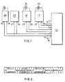
- a microprocessor 10 has a plurality of ports 11 - 16 for the input and output of signals to and from the microprocessor.
- the microprocessor is controlled to output clock signals on ports 11,13 and 15 and to configure the ports 12, 14 and 16 as input/output terminals for signals relating to data transfer.
- the ports of the microprocessor handle both input and output of signals and hence are dual direction ports. Accordingly the microprocessor 10 is a device having this dual direction port characteristic.
- a suitable component for use as the microprocessor 10 is available commercially under the type number 80C154 JS.
- the franking machine is provided with two separate memory devices 17, 18 which respectively have terminals 19, 20 for the input of clock signals and terminals 21, 22 for the input and output of signals relating to data transfer.
- the memory devices include control and address circuits which respond to a predetermined format of signals for the transfer of data to and from storage locations within the memory devices.
- a suitable commercially available component for the memory devices is that marketed by Philips under the type number PCF 8570. The format of signals and the operations of reading and writing data from and to the storage locations will be described hereinafter.
- the ports 11, 12 of the microprocessor 10 are connected respectively to the terminals 19 and 21 of memory device 17 and the ports 13, 14 of the microprocessor are connected respectively to the terminals 20, 22 of the memory device 18.
- the memory devices 17, 18 receive clock signals on terminals 19, 20 and have their terminals 21, 22 connected to the microprocessor ports for the transfer of signals relating to data transfer to and from the microprocessor.
- Each of the memory devices 17, 18 includes a first set of storage locations designated to provide a descending register, an ascending register and a tote or item count register.
- each memory device includes a second set of storage locations designated to provide a duplicate descending register, a duplicate ascending register and a duplicate tote register.
- each of the registers is implemented in each of four set of storage locations, two sets of locations in each of two memory devices.
- the construction of the memory devices is such that data is retained in the storage locations only when power is applied to the memory devices. Accordingly, in order to ensure that data is not lost when the franking machine is switched off or in the event of a power failure, batteries 23,24 are provided to power the memory devices in an inactive mode to ensure that the memory devices are always energised with power. In this inactive mode the memory devices are incapable of being accessed and accordingly they are immune to any signals which may be induced by stray signals on their terminals 21, 22. As a result there is little risk of corruption of data stored in the memory devices during any period when the franking machine is switched off. In this inactive mode the memory devices require very little power and hence the batteries have an extremely long operational life.
- the format of signals used in data transfer between the microprocessor and the memory devices is shown in Figure 2.
- the microprocessor acts as a master and controls the reading and writing of data from and to the storage locations of the memory devices by a string of signals in the format shown in Figure 2. Reading or writing to both memory devices is accomplished in the same manner and, by way of illustration, reading and writing from a storage location in memory device 17 will now be described. Reading or writing is initiated by a start bit 'S' input on terminal 21 and is followed by signals representing an address of for example 7 bits corresponding to the memory device 17. The next bit 'W' of the string determines the direction of transfer between the microprocessor and the memory device of the succeeding block of signals.
- the next block of signals will represent a storage location within the memory device 17 to which data is to be written or from which data is to be read by the microprocessor and hence this bit "W" has a value, for example '0', which determines that the succeeding block will be transferred in a direction from the microprocessor to the memory device.
- the memory device Prior to transmission of the address of the storage location, the memory device sends an acknowledgement signal 'A' to the microprocessor. On receipt of the acknowledgement signal 'A', the microprocessor transmits the desired storage location addresses to the memory device 17 . A further acknowledgement signal 'A' is then sent back to the microprocessor by the memory device 17. The start bit 'S' is repeated by the microprocessor followed by the address corresponding to the memory device 17.
- a bit 'R/W' having a value '1' or '0' depending upon whether data is to be read from or written to the addressed storage location in the memory device 17 is sent by the microprocessor.
- the microprocessor receives or transmits one or more blocks of data read from or to be written into the addressed storage location, each block of data being followed by an acknowledgement 'A' from the memory device 17.
- a stop bit 'P' is sent by the microprocessor to terminate access to the memory device.
- the string of signals is transmitted between the port 14 of the microprocessor and the terminal 22 of the device 18.
- the string after the start bit 'S' will include an address corresponding to the memory device 18. Thereafter, transmission of data in either direction is effected as described above in relation to transfers between the microprocessor and memory device 17.
- more than one device may be connected to one port of the microprocessor as is described hereinafter in relation to a third pair of ports 15, 16.
- the third pair of ports 15, 16 of the microprocessor 10 are provided for communication with a keyboard and display unit 25.
- Clock signals are transmitted by the microprocessor 10 via port 15 to a terminal 26 of the keyboard and display unit 25.
- Signals relating to data transfer between the microprocessor 10 and the display device 25 are carried via port 16 and a terminal 27 of the device 25.
- Data transfers between the microprocessor and the device 25 are effected in a similar manner as described above in relation to reading and writing data in the memory devices 17, 18.
- further devices may be connected to the ports 15, 16.
- a real time clock device 28 may be provided.
- the device 28 has terminals 29, 30 respectively for clock signals and real time data signals.
- the microprocessor desires to access the device 28 to read out real time data signals therefrom, the microprocessor, after transmitting a start signal 'S', transmits a device address signal corresponding to the device address of the device 28.
- the device 28 Upon receipt of this device address signal, the device 28 sends back an acknowledgement signal 'A' as hereinbefore described in relation to accesses of the memory devices 17, 18.
- the devices 25 and 28 respond only to device address signals corresponding to the respective devices and hence if one device is addressed, the other device does not respond or become activated.
- a device address signal may be utilised to determine which of a number of possible devices is or are connected to the port of the microprocessor. For example if it is desired to provide the franking machine with a selected one of a number of differing versions of a device, each version is configured to have a different device address. This may be effected by selective hardwiring of the addresses in the different versions of the device.
- the microprocessor sends a message containing a device address signal corresponding to one of the possible versions of the device.
- the microprocessor If the device address signal corresponds to the device address of that version of device installed in the franking machine an acknowledgement signal is returned by the device to the microprocessor and the microprocessor then selects a software program routine corresponding to that version of the device. However if no acknowledgement is received within a predetermined time interval, the microprocessor sends a message containing a device address corresponding to another possible version of the device. If there are only two possible versions of the device, this second message will result in return of an acknowledgement by the device. However if there are a larger number of possible versions of the device, the microprocessor continues to send messages containing device addresses in turn corresponding to other versions of the device until an acknowledgement is received back from the device.
- Receipt of an acknowledgement serves to confirm the version of device installed and the software routine is selected accordingly. If after all the devices addresses have been included in turn in the messages and no acknowledgement is returned, a fault condition exists and this will be indicated by an appropriate signal or indication to the user of the franking machine.
- the recognition by the microprocessor of which one of a number of differing devices is installed is beneficial in enabling the construction of franking machines providing differing user facilities utilising units providing these differing facilities together with other units providing functions required in common for a range of franking machines.
- a range of franking machines may be constructed using the same unit containing the microprocessor for carrying out accounting and control functions while providing variations in facilities to the user by the provision of differing versions of the keyboard and display device.
- the operation of the microprocessor in carrying out accounting and control functions and in effecting data transfers between the microprocessor and the memory devices and display unit 25 is controlled by a program stored in non-volatile memory (not shown). It will be understood that, since a user of the franking machine selects desired modes of operation of the machine and inputs data such as franking values required by means of the keyboard of the unit 25, the microprocessor is controlled by its program to periodically carry out a read operation in respect of the unit 25 to ascertain whether any key has been operated by a user.
- the microprocessor In carrying out accounting functions which depend upon a value stored in any register of the memory devices 17, 18 the microprocessor is caused to access in turn all storage locations comprising replications of that register in both memory devices to check that the values in all replications of that register are identical and when a new value is written to a register, all the replications of that register are addressed in turn by the microprocessor to write the new value in each of the replications of the register.
- microprocessor devices may be provided and each microprocessor may be allocated to perform selected ones of the accounting and control functions.
- the microprocessors may be interconnected in the same manner that the microprocessor 10 is connected to the devices 17, 18, 25 and 28.
- An arrangement incorporating two microprocessors is shown in Figure 3.
- Microprocessors 31, 32 have pairs of ports 33, 34 and 35, 36 respectively which are interconnected. Ports 33 and 35 carry clock signals from one microprocessor to the other and ports 34, 36 carry data signals between the microprocessors.
- the microprocessor 31 has other pairs of ports connected to a memory device 37, a display and keyboard device 38 and a real time clock device 39 as has been described hereinbefore with reference to Figure 1.
- Microprocessor 32 has a pair of ports connected to a second memory device 40 and in addition has a further pair of ports 41, 42 which may be used for connection to any other required device for example a driver device for a printer or an interface device for communication with devices external to the franking machine.
- the microprocessor 31 is controlled by software to perform functions related to the keyboard and display device 38 such as responding to input signals generated by operation of keys by a user and displaying data and information on the display for instruction of a user of the franking machine.
- the performance of accounting functions may be allocated to either one of the microprocessors 31, 32, the results of accounting being written directly to the memory device connected to the microprocessor and in addition being sent to the other microprocessor for writing into the memory device connected to the other microprocessor.
- both microprocessors may be controlled to perform accounting functions and the results from both microprocessors may be compared to check that the function has been correctly performed before writing the accounting data to the respective memory devices.
- the microprocessor 32 is controlled by software to operate a printer driver connected to ports 41, 42 to print a franking impression on a mail item being franked.
- the microprocessor requiring to send or receive data to or from the other microprocessor acts as a so-called master device and sends clock signals to the other microprocessor and controls data transfer as described hereinbefore, the other microprocessor then acting as a slave device in the same manner as, for example, the memory devices in relation to data transfer between a microprocessor and the memory device.
- the master slave relationship is determined by which microprocessor calls for a data transfer and is not dependent upon the direction of data transfer. It will be appreciated that more than two microprocessors may be provided and the microprocessors and other devices may be connected in configurations other than that shown in Figure 3 .
- a pair of connections 43, 44 to a port of the microprocessor of a franking machine 45 may be utilised to connect to similar ports of microprocessors of external systems or to terminals of external passive devices 46 as shown in Figure 4.
- a single pair of connections, one connection 43 for clock signals and the other connection 44 for data signals may be utilised to interconnect a number of external systems or devices 46 with the franking machine 45.
Landscapes
- Physics & Mathematics (AREA)
- General Physics & Mathematics (AREA)
- Engineering & Computer Science (AREA)
- Computer Hardware Design (AREA)
- General Engineering & Computer Science (AREA)
- Communication Control (AREA)
Claims (8)
- Frankiermaschine mit einer elektronischen Einrichtung (17,18), welche ein erstes Terminal (21,22) zur Ein- und Ausgabe von Daten- und Steuersignalen, ein zweites Terminal (19,20) zur Eingabe von Zeitsignalen und einen elektronischen Mikroprozessor (10) aufweist, wobei der Mikroprozessor (10) erste und zweite Anschlüsse aufweist, wobei der erste Anschluß (12,14) außerhalb des Mikroprozessors mit dem ersten Terminal (21,22) verbunden ist und der zweite Anschluß (11,13) außerhalb des Mikroprozessors mit dem zweiten Terminal (19,20) verbunden ist, wobei der erste Anschluß zur Eingabe und Ausgabe der Daten und Steuersignale allein mit dem ersten Terminal verbunden ist, wobei die elektronische Einrichtung (17,18) eine Einrichtungsadressenanzeige aufweist, welche diese Einrichtung (17,18) identifiziert, und wobei der Mikroprozessor (10) zur Übertragung eines Einrichtungsadressensignales und von Steuersignalen zu der elekronischen Einrichtung über den ersten Anschluß und die erste Verbindung gesteuert wird, wobei die elektronische Einrichtung (17,18) betätigbar ist, um Daten repräsentierende Signale nur in Antwort auf die Übereinstimmung zwischen dem ersten Einrichtungsadressensignal und der ersten Einrichtungsadresse zu empfangen, wobei die elektronische Einrichtung (17,18) betätigbar ist, nach Empfang eines mit der Einrichtungsadresse übereinstimmenden Einrichtungsadressensignals ein Betätigungssignal über das erste Terminal (21,22) und die erste Verbindung zu dem ersten Anschluß (12,14) des Mikroprozessors (10) zurückzuschicken und wobei der Mikroprozessor (10) in Antwort auf dieses Bestätigungssignal betätigbar ist, um die Daten repräsentierenden Signale zwischen dem Mikroprozessor (10) und der elektronischen Einrichtung (17,18) über den ersten Anschluß (12,14) und die erste Verbindung zu übertragen.
- Frankiermaschine mit einer elektronischen Einrichtung (17,18), welche ein erstes Terminal (21,22) zur Ein- und Ausgabe von Daten- und Steuersignalen, ein zweites Terminal (19,20) zur Eingabe von Zeitsignalen und einen elektronischen Mikroprozessor (10) aufweist, wobei der Mikroprozessor (10) erste und zweite Anschlüsse aufweist, wobei der erste Anschluß (12,14) außerhalb des Mikroprozessors zur Ein- und Ausgabe der Daten- und Steuersignale mit dem ersten Terminal (21,22) verbunden ist und wobei der zweite Anschluß (11,13) außerhalb des Mikroprozessors zur Ausgabe der Zeitsignale mit dem zweiten Terminal (19,20) verbunden ist, wobei die elektronische Einrichtung (17,18) eine Einrichtungsadressenanzeige zur Identifizierung der Einrichtung (17,18) aufweist und wobei der Mikroprozessor (10) gesteuert wird, um ein Einrichtungsadressensignal und Steuersignale zur elektronischen Einrichtung über den ersten Anschluß und die erste Verbindung zu übertragen, wobei die elektronische Einrichtung (17,18) betätigbar ist, um Daten repräsentierende Signale nur in Antwort auf die Übereinstimmung zwischen dem Einrichtungsadressensignal und der Einrichtungsadresse zu empfangen, wobei die elektronische Einrichtung (17,18) betätigbar ist, nach Empfang eines mit der Einrichtungsadresse übereinstimmenden Einrichtungsadressensignales ein Bestätigungssignal über das erste Terminal (19,20) und die erste Verbindung zu dem ersten Anschluß (11,13) des Mikroprozessors (10) zurückzuschicken, wobei der Mikroprozessor in Antwort auf das Bestätigungssignal betätigbar ist, um die Daten repräsentierenden Signale zwischen dem Mikroprozessor (10) und der elektronischen Einrichtung (17,18) über den ersten Anschluß (12,14) und die erste Verbindung zu übertragen, wobei Mittel zur Steuerung des Mikroprozessors (10) vorgesehen sind, die eine Initialisierungsroutine ausführen, welche das Absenden einer ersten, ein erstes Einrichtungsadressensignal enthaltenden Nachricht zur Einrichtung (17,18) einschließt, wobei die Einrichtung (17,18) in Antwort auf ein der Einrichtungsadresse entsprechendes Einrichtungsadressensignal betätigbar ist, um ein Bestätigungssignal zum Mikroprozessor (10) zurückzusenden, wobei der Mikroprozessor (10) in Antwort auf das Bestätigungssignal betätigbar ist, um die Initialisierungsroutine fortzusetzen.
- Frankiermaschine nach Anspruch 2,
dadurch gekennzeichnet,
daß der Mikroprozessor (10) in Abwesenheit eines Bestätigungssignals innerhalb eines vorbestimmten Zeitintervalls betätigbar ist, um eine zweite, ein zweites Adressensignal enthaltende Nachricht zur Einrichtung (17,18) zu senden und daß die Einrichtung (17,18) in Antwort auf ein der Einrichtungsadresse entsprechendes zweites Einrichtungsadressensignal betätigbar ist, um ein Bestätigungssignal zum Mikroprozessor (10) zurückzusenden. - Frankiermaschine nach Anspruch 2 oder 3,
dadurch gekennzeichnet,
daß die elektronische Einrichtung (17,18) eine aus einer Mehrzahl von Einrichtungen ausgewählte Einrichtung ist, wobei jede dieser Einrichtungen aus der Mehrzahl von Einrichtungen jeweils eine unterschiedliche Einrichtungsadressenanzeige einschließt, daß der Mikroprozessor (10) von der Initialisierungsroutine zur Aussendung einer Folge von Nachrichten zur elektronischen Einrichtung (17,18) gesteuert wird, wobei jede Nachricht ein unterschiedliches Adressensignal enthält, wobei Mittel zur Speicherung einer Mehrzahl von Softwareroutinen, die jeweils mit den verschiedenen Einrichtungen verbunden sind, vorgesehen sind, und wobei der Mikroprozessor (10) nach Empfang eines Bestätigungssignals in Antwort zur Aussendung einer Nachricht betätigbar ist, die ein Adressensignal enthält, welche mit der Einrichtungsadressenanzeige der ausgewählten Einrichtung (17,18) übereinstimmt, um die mit dieser ausgewählten Einrichtung (17,18) verbundene Softwareroutine auszuwählen. - Frankiermaschine nach irgendeinem der Ansprüche 2, 3 oder 4,
dadurch gekennzeichnet,
daß die elektronische Einrichtung eine Anzeigeeinrichtung aufweist. - Frankiermaschine nach irgendeinem der Ansprüche 1 bis 4,
dadurch gekennzeichnet,
daß die elektronische Einrichtung (17,18) einen Speicher mit einer Mehrzahl von Datenspeicherorten aufweist, und daß der Mikroprozessor (10) betätigbar ist, um über den ersten Anschluß (12,14) und die erste Verbindung zum ersten Terminal (21,22) ein Speicherortadressensignal zu übertragen, um einen der Datenspeicherorte auszuwählen und danach einen Datentransfer zwischen dem ausgewählten Datenspeicherort und dem Mikroprozessor (10) auszuführen. - Frankiermaschine nach irgendeinem der vorangehenden Ansprüche,
gekennzeichnet durch
eine Mehrzahl von elektronischen Einrichtungen (17,18), welche jeweils durch verschiedene Einrichtungsadressen identifiziert werden und jeweils erste und zweite Terminals (21,22;19,20) aufweisen, wobei der Mikroprozessor (10) eine Mehrzahl von Paaren von ersten und zweiten Anschlüssen (12,11;14,13) und wobei eine Mehrzahl von ersten Verbindungsmitteln die ersten Anschlüsse jeweils mit einem jeweils verschiedenen ersten Terminal verbindet, wobei der erste Anschluß jeweils nur mit einem ersten Terminal verbunden ist, und wobei eine Mehrzahl von zweiten Verbindungsmitteln die zweiten Anschlüsse mit jeweils einem verschiedenen zweiten Terminal verbindet, wobei jeder zweite Anschluß jeweils nur mit einem zweiten Terminal verbunden ist, wobei der Mikroprozessor (10) gesteuert wird, um einen Datentransfer mit einer ausgewählten der elektronischen Einrichtungen (17,18) durch Auswahl eines Paares von ersten und zweiten Anschlüssen, Übertragung über den ausgewählten ersten Anschluß zur ausgewählten Einrichtung eines Adressensignals in Übereinstimmung mit der Einrichtungsadresse der ausgewählten Einrichtung zu bewirken und in Antwort auf den Empfang eines Bestätigungssignals bei dem ausgewählten ersten Anschluß Daten zwischen der ausgewählten Einrichtung (17,18) und dem Mikroprozessor (10) zu übertragen. - Frankiermaschine nach Anspruch 7,
dadurch gekennzeichnet,
daß wenigstens eine der elektronischen Einrichtungen ein weiterer Mikroprozessor (32) ist.
Applications Claiming Priority (2)
| Application Number | Priority Date | Filing Date | Title |
|---|---|---|---|
| GB888819647A GB8819647D0 (en) | 1988-08-18 | 1988-08-18 | Franking machine |
| GB8819647 | 1988-08-18 |
Publications (3)
| Publication Number | Publication Date |
|---|---|
| EP0356052A2 EP0356052A2 (de) | 1990-02-28 |
| EP0356052A3 EP0356052A3 (en) | 1990-08-29 |
| EP0356052B1 true EP0356052B1 (de) | 1994-06-08 |
Family
ID=10642342
Family Applications (1)
| Application Number | Title | Priority Date | Filing Date |
|---|---|---|---|
| EP89307968A Expired - Lifetime EP0356052B1 (de) | 1988-08-18 | 1989-08-04 | Frankiermaschine |
Country Status (4)
| Country | Link |
|---|---|
| US (1) | US5128875A (de) |
| EP (1) | EP0356052B1 (de) |
| DE (1) | DE68915895T2 (de) |
| GB (1) | GB8819647D0 (de) |
Families Citing this family (7)
| Publication number | Priority date | Publication date | Assignee | Title |
|---|---|---|---|---|
| FR2664407B1 (fr) * | 1990-07-04 | 1992-09-11 | Alcatel Satmam | Machine a affranchir le courrier, comportant un circuit integre specifique constituant des interfaces. |
| GB9020596D0 (en) * | 1990-09-21 | 1990-10-31 | Alcatel Business Systems | Data transmission method and apparatus |
| US5276844A (en) * | 1991-08-05 | 1994-01-04 | Ascom Autelca Ltd. | Protection system for critical memory information |
| EP0615211B1 (de) * | 1993-03-11 | 1998-02-04 | Francotyp-Postalia Aktiengesellschaft & Co. | Verfahren zum Speichern sicherheitsrelevanter Daten |
| US5666292A (en) * | 1994-12-13 | 1997-09-09 | Pitney Bowes Inc. | External interface unit having message routing and protocol conversion |
| US6907634B2 (en) * | 2001-05-01 | 2005-06-21 | Milliken & Company | Patterning system using a limited number of process colors |
| KR101563685B1 (ko) * | 2009-02-12 | 2015-10-28 | 삼성전자주식회사 | 멀티 디스플레이 장치 |
Family Cites Families (8)
| Publication number | Priority date | Publication date | Assignee | Title |
|---|---|---|---|---|
| US4148099A (en) * | 1978-04-11 | 1979-04-03 | Ncr Corporation | Memory device having a minimum number of pins |
| US4525785A (en) * | 1979-10-30 | 1985-06-25 | Pitney Bowes Inc. | Electronic postage meter having plural computing system |
| US4916623A (en) * | 1982-01-29 | 1990-04-10 | Pitney Bowes Inc. | Electronic postage meter having redundant memory |
| CA1206619A (en) * | 1982-01-29 | 1986-06-24 | Frank T. Check, Jr. | Electronic postage meter having redundant memory |
| US4535419A (en) * | 1982-10-22 | 1985-08-13 | Pitney Bowes Inc. | System and method for computing fractional postage values |
| US4713769A (en) * | 1985-09-11 | 1987-12-15 | Pitney Bowes Inc. | Method and apparatus for locating and displaying historical information within an electronic postage meter |
| US4742469A (en) * | 1985-10-31 | 1988-05-03 | F.M.E. Corporation | Electronic meter circuitry |
| FR2620259B1 (fr) * | 1987-03-31 | 1989-11-24 | Smh Alcatel | Dispositif de couplage de memoires non volatiles dans une machine electronique et machine a affranchir en faisant application |
-
1988
- 1988-08-18 GB GB888819647A patent/GB8819647D0/en active Pending
-
1989
- 1989-08-04 DE DE68915895T patent/DE68915895T2/de not_active Expired - Fee Related
- 1989-08-04 EP EP89307968A patent/EP0356052B1/de not_active Expired - Lifetime
- 1989-08-08 US US07/390,822 patent/US5128875A/en not_active Expired - Lifetime
Also Published As
| Publication number | Publication date |
|---|---|
| EP0356052A3 (en) | 1990-08-29 |
| DE68915895D1 (de) | 1994-07-14 |
| US5128875A (en) | 1992-07-07 |
| DE68915895T2 (de) | 1995-01-05 |
| EP0356052A2 (de) | 1990-02-28 |
| GB8819647D0 (en) | 1988-09-21 |
Similar Documents
| Publication | Publication Date | Title |
|---|---|---|
| US4858138A (en) | Secure vault having electronic indicia for a value printing system | |
| US5200903A (en) | Franking machine | |
| US4301507A (en) | Electronic postage meter having plural computing systems | |
| US4809185A (en) | Secure metering device storage vault for a value printing system | |
| US5206812A (en) | Franking machine | |
| US5535279A (en) | Postage accounting system including means for transmitting a bit-mapped image of variable information for driving an external printer | |
| US5688056A (en) | Method for controlling a printer in order to obtain postages | |
| CA2164892C (en) | Postage accounting system including means for transmitting ascii encoded variable information for driving an external printer | |
| US4308579A (en) | Multiprocessor parcel postage metering system having serial data bus | |
| US4410962A (en) | Mailing system interface interconnecting incompatible communication systems | |
| US5323323A (en) | Franking machine system | |
| US4566106A (en) | Electronic postage meter having redundant memory | |
| CA2164890C (en) | Postage metering system with dedicated and non-dedicated postage printing means | |
| GB2215888A (en) | Fault tolerant smart card | |
| EP0513880B1 (de) | Mikroprozessorsysteme für Frankiermaschinenanordnungen | |
| US4395756A (en) | Processor implemented communications interface having external clock actuated disabling control | |
| US4506329A (en) | Non-volatile memory serial number lock for electronic postage meter | |
| EP0356052B1 (de) | Frankiermaschine | |
| EP0516403A2 (de) | Ferndiagnoseverfahren für Frankiermaschine | |
| US4916623A (en) | Electronic postage meter having redundant memory | |
| US4498187A (en) | Electronic postage meter having plural computing systems | |
| EP0194658A2 (de) | Frankiermaschine mit Auswahlmittel für nichtflüchtigen Speicher | |
| WO1986000734A1 (en) | High speed data transfer between first and second processing means | |
| US5109507A (en) | Electronic postage meter having redundant memory | |
| EP0285390B1 (de) | Frankiermaschine |
Legal Events
| Date | Code | Title | Description |
|---|---|---|---|
| PUAI | Public reference made under article 153(3) epc to a published international application that has entered the european phase |
Free format text: ORIGINAL CODE: 0009012 |
|
| AK | Designated contracting states |
Kind code of ref document: A2 Designated state(s): DE FR GB |
|
| PUAL | Search report despatched |
Free format text: ORIGINAL CODE: 0009013 |
|
| AK | Designated contracting states |
Kind code of ref document: A3 Designated state(s): DE FR GB |
|
| 17P | Request for examination filed |
Effective date: 19901221 |
|
| 17Q | First examination report despatched |
Effective date: 19920703 |
|
| RAP1 | Party data changed (applicant data changed or rights of an application transferred) |
Owner name: NEOPOST LIMITED |
|
| GRAA | (expected) grant |
Free format text: ORIGINAL CODE: 0009210 |
|
| AK | Designated contracting states |
Kind code of ref document: B1 Designated state(s): DE FR GB |
|
| ET | Fr: translation filed | ||
| REF | Corresponds to: |
Ref document number: 68915895 Country of ref document: DE Date of ref document: 19940714 |
|
| PLBE | No opposition filed within time limit |
Free format text: ORIGINAL CODE: 0009261 |
|
| STAA | Information on the status of an ep patent application or granted ep patent |
Free format text: STATUS: NO OPPOSITION FILED WITHIN TIME LIMIT |
|
| 26N | No opposition filed | ||
| REG | Reference to a national code |
Ref country code: GB Ref legal event code: IF02 |
|
| PGFP | Annual fee paid to national office [announced via postgrant information from national office to epo] |
Ref country code: DE Payment date: 20050818 Year of fee payment: 17 |
|
| PGFP | Annual fee paid to national office [announced via postgrant information from national office to epo] |
Ref country code: FR Payment date: 20050819 Year of fee payment: 17 |
|
| PGFP | Annual fee paid to national office [announced via postgrant information from national office to epo] |
Ref country code: GB Payment date: 20050822 Year of fee payment: 17 |
|
| PG25 | Lapsed in a contracting state [announced via postgrant information from national office to epo] |
Ref country code: DE Free format text: LAPSE BECAUSE OF NON-PAYMENT OF DUE FEES Effective date: 20070301 |
|
| GBPC | Gb: european patent ceased through non-payment of renewal fee |
Effective date: 20060804 |
|
| REG | Reference to a national code |
Ref country code: FR Ref legal event code: ST Effective date: 20070430 |
|
| PG25 | Lapsed in a contracting state [announced via postgrant information from national office to epo] |
Ref country code: GB Free format text: LAPSE BECAUSE OF NON-PAYMENT OF DUE FEES Effective date: 20060804 |
|
| PG25 | Lapsed in a contracting state [announced via postgrant information from national office to epo] |
Ref country code: FR Free format text: LAPSE BECAUSE OF NON-PAYMENT OF DUE FEES Effective date: 20060831 |