EP0353421A2 - Printed circuit board connection - Google Patents
Printed circuit board connection Download PDFInfo
- Publication number
- EP0353421A2 EP0353421A2 EP89110338A EP89110338A EP0353421A2 EP 0353421 A2 EP0353421 A2 EP 0353421A2 EP 89110338 A EP89110338 A EP 89110338A EP 89110338 A EP89110338 A EP 89110338A EP 0353421 A2 EP0353421 A2 EP 0353421A2
- Authority
- EP
- European Patent Office
- Prior art keywords
- printed circuit
- circuit board
- spring biased
- connector
- nose piece
- Prior art date
- Legal status (The legal status is an assumption and is not a legal conclusion. Google has not performed a legal analysis and makes no representation as to the accuracy of the status listed.)
- Ceased
Links
Images

Classifications
-
- H—ELECTRICITY
- H01—ELECTRIC ELEMENTS
- H01R—ELECTRICALLY-CONDUCTIVE CONNECTIONS; STRUCTURAL ASSOCIATIONS OF A PLURALITY OF MUTUALLY-INSULATED ELECTRICAL CONNECTING ELEMENTS; COUPLING DEVICES; CURRENT COLLECTORS
- H01R12/00—Structural associations of a plurality of mutually-insulated electrical connecting elements, specially adapted for printed circuits, e.g. printed circuit boards [PCB], flat or ribbon cables, or like generally planar structures, e.g. terminal strips, terminal blocks; Coupling devices specially adapted for printed circuits, flat or ribbon cables, or like generally planar structures; Terminals specially adapted for contact with, or insertion into, printed circuits, flat or ribbon cables, or like generally planar structures
- H01R12/70—Coupling devices
- H01R12/7005—Guiding, mounting, polarizing or locking means; Extractors
-
- H—ELECTRICITY
- H05—ELECTRIC TECHNIQUES NOT OTHERWISE PROVIDED FOR
- H05K—PRINTED CIRCUITS; CASINGS OR CONSTRUCTIONAL DETAILS OF ELECTRIC APPARATUS; MANUFACTURE OF ASSEMBLAGES OF ELECTRICAL COMPONENTS
- H05K1/00—Printed circuits
- H05K1/02—Details
- H05K1/11—Printed elements for providing electric connections to or between printed circuits
- H05K1/117—Pads along the edge of rigid circuit boards, e.g. for pluggable connectors
-
- H—ELECTRICITY
- H01—ELECTRIC ELEMENTS
- H01R—ELECTRICALLY-CONDUCTIVE CONNECTIONS; STRUCTURAL ASSOCIATIONS OF A PLURALITY OF MUTUALLY-INSULATED ELECTRICAL CONNECTING ELEMENTS; COUPLING DEVICES; CURRENT COLLECTORS
- H01R13/00—Details of coupling devices of the kinds covered by groups H01R12/70 or H01R24/00 - H01R33/00
- H01R13/62—Means for facilitating engagement or disengagement of coupling parts or for holding them in engagement
- H01R13/629—Additional means for facilitating engagement or disengagement of coupling parts, e.g. aligning or guiding means, levers, gas pressure electrical locking indicators, manufacturing tolerances
- H01R13/631—Additional means for facilitating engagement or disengagement of coupling parts, e.g. aligning or guiding means, levers, gas pressure electrical locking indicators, manufacturing tolerances for engagement only
-
- H—ELECTRICITY
- H05—ELECTRIC TECHNIQUES NOT OTHERWISE PROVIDED FOR
- H05K—PRINTED CIRCUITS; CASINGS OR CONSTRUCTIONAL DETAILS OF ELECTRIC APPARATUS; MANUFACTURE OF ASSEMBLAGES OF ELECTRICAL COMPONENTS
- H05K2201/00—Indexing scheme relating to printed circuits covered by H05K1/00
- H05K2201/20—Details of printed circuits not provided for in H05K2201/01 - H05K2201/10
- H05K2201/2027—Guiding means, e.g. for guiding flexible circuits
-
- Y—GENERAL TAGGING OF NEW TECHNOLOGICAL DEVELOPMENTS; GENERAL TAGGING OF CROSS-SECTIONAL TECHNOLOGIES SPANNING OVER SEVERAL SECTIONS OF THE IPC; TECHNICAL SUBJECTS COVERED BY FORMER USPC CROSS-REFERENCE ART COLLECTIONS [XRACs] AND DIGESTS
- Y10—TECHNICAL SUBJECTS COVERED BY FORMER USPC
- Y10S—TECHNICAL SUBJECTS COVERED BY FORMER USPC CROSS-REFERENCE ART COLLECTIONS [XRACs] AND DIGESTS
- Y10S439/00—Electrical connectors
- Y10S439/951—PCB having detailed leading edge
Definitions
- the present invention relates to the connection of a printed circuit board connector with a printed circuit board connector, and more particularly relates to an improved edge design of the edge of the printed circuit board for use with printed circuit board connectors.
- Printed circuit board connectors are known in which spring members urge electrical contact members into electrial connection with input/output means such as gold tabs on the printed circuit board as the edge of the printed circuit board is inserted into the connector.
- the edge of the printed circuit board is typically beveled to push the spring loaded electrical contact member into a contacting position as the edge of the printed circuit board moves past the electrical contact member.
- the beveling of the edge of the printed circuit board exposes the ends of glass fibers in the substrate of the printed circuit board such that as the beveled edge of the printed circuit board pushes past the spring loaded electrical contact member, the ends of the glass fibers damage the electrical contact member.
- the damaged electrical contact member then moves over the gold tabs of the printed circuit board, it in turn damages the gold tabs. This damage severely limits the number of times which a printed circuit board may be plugged into a printed circuit board connector before failure.
- US-A-3 951 492 discloses a printed circuit board connector in which the leading edge of the printed circuit board bows a contact to make an electrical connection.
- US-A-4 157 857 discloses a printed circuit board connector in which electrical connection is made with a gold contact on the edge of the printed circuit board as it is inserted into the connector.
- the connector is designed to minimize wear as the board is forced into the connector.
- US-A-4 221 448 discloses a connector having a resilient contact which is designed to make electrical contact with a conductor pad on the side of a printed circuit board as the printed circuit board is inserted into the connector.
- the edge of the printed circuit board is designed to co-act with the resilient contact such that a bulge on the resilient contact applies increasing lateral force against the conductor pad as the board continues to be inserted.
- US-A-4 572 604 discloses an electrical connector for the terminating edge of a printed circuit board which, when connected to the terminating edge of the printed circuit board, engages bowed portions of contact fingers in a card edge connector.
- the leading edge of the electrical connector when connected to the printed circuit board, includes a bevel for guiding the connector into the card slot of a conventional printed circuit board card edge connector.
- US-A-4 613 193 and US-A-4 634 210 each discloses another printed circuit board connector in which the leading edge of the printed circuit board activates an activating mechanism to move contacts into electrical connection with conductor pads on the sides of the printed circuit board as the printed circuit board is inserted into the connector.
- the invention as claimed solves the problem to provide an improved printed circuit board which may be repeatedly pluged into and removed from a printed circuit board edge connector without damaging the electrical contacts of the connector.
- the present invention relates to an improved printed circuit board design in which a nose piece is bonded to the leading edge of the printed circuit board such that electrical contacts of a connector are not damaged as the printed circuit board is inserted into the connector.
- the nose piece is made of a lubritious, insulating material for deflecting the spring biased contact members without cousing damage to the members or the electrical contacts thereon.
- each spring biased member is fixed in the connector at one end and has a bent portion with an electrical contact on the bent portion.
- the electrical contact is in a impact protected position when its spring biased member is undeflected, and moves to a contact making position for contact with an input/output tab on the printed circuit board as the spring biased member is deflected around its fixed end during the plugging in operation of the printed circuit board.
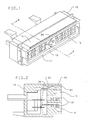
- Fig. 1 is a perspective drawing of a connector 10 having a spade connector portion 12 and a printed circuit board edge connector portion 14.
- the spade connector portion 12 includes a plurality of openings such as opening 15, each containing jaws designed to resiliently grip and make electrical contact with a spade (not shown) inserted into the opening 15.
- the openings 15 are arranged in the spade connector portion 12 in a socket 18 designed such that when a socket of a mating connector (not shown) is engaged with the connector 10, the holes 15 are aligned with spade connectors for making electrical connections.
- Any number of known connectors, such as the spade connector shown and described, may be used with the present invention with equal facility.
- the present invention is not limited to use with any particular connector and may, in fact, be used with any connector design, or may be used alone as a printed circuit board edge connector.
- the printed circuit board connector 14 is provided for plugging a printed circuit board into the connector 10 separate and apart from the connections made by connector portion 12.
- the printed circuit board edge connector portion 14 is formed on one side of the connector 10, and includes a slot or slots 20 having a beveled mouth or opening 21 (see Fig. 2) for guiding the leading edge of a printed circuit board into the slot 20. As shown in Fig. 2, a plurality of spring members 23 are located in the slot 20 and include a contact portion, to be discussed later, for making electrical contact with conductor tabs on the side of the printed circuit board. As the disclosed printed circuit board edge connector portion 14 is designed to have a minimum width, there is not enough room to include within the connector portion 14 reduced or zero force insertion mechanisms as are found in prior art printed circuit board edge connectors.
- the holes 15 contain clips 24 for engaging spades (not shown) which are inserted into the holes 15 when an electrical connection is made by the spade connector portion 12.
- Fig. 3 is an elevational view of a partial section of the connector 10 having a printed circuit board 25 partially inserted into the slot 20, and showing one of the spring members 23 of Fig. 1.
- the circuit board 25 has a nose piece 26 bonded on its leading edge 28.
- both the leading edge 28 and the nose 26 have cooperating stepped portions 29 and 30, respectively, forming a babbit type joint.
- the forward portion of the nose piece 26 is slanted at 32 to cooperate with a bent portion 34 of the spring member 23.
- the spring member 23 is fixed at one end 35 (see Figs.
- the printed circuit board has a number of gold tabs 38 as part of its printed electrical circuit, typically one for each spring member 23.
- the spring member 23 carries an electrical contact 36 which, when the printed circuit board 25 is fully inserted into the slot 20, makes electrical contact with a respective one of the gold tabs 38 (see Fig 4).
- the electrical contact 36 is located on the bent portion 34 of the spring member 23, and is positioned such that the electrical contact 36 is protected from the initial impact between the bent portion 34 and the slanted portion 32 of the nose piece 26 as the printed circuit board 25 is plugged into the connector portion 14. As the spring member 23 is deflected around its fixed end 35, the electrical contact 36 is moved from its impact protected position to a contact making position for making an electrical connection with the gold tab 38. This design minimizes wear on the tab 38 and the electrical contact 36 while allowing wiping action between them to make a good electrical contact.
- the spring member 23 is made of a bronze alloy and the electrical contact 36 may be gold plated to provide the desired electrical characteristics of the contact-to-tab connection when the printed circuit board is fully inserted into the slot 20.
- the tabs 38 form a part, such as input or output connections, of a electrical circuit printed on the printed circuit board 25.
- Each of the tabs 38 are spaced to be aligned with respective ones of the spring members 23 as the printed circuit board is inserted into the slot 20 such that the contacts 36 may make electrical connection with selected ones of the tabs 38, as desired.
- the nose piece 26 is made of a lubritious material to further minimize mechanical damage to the electrical contact 36 during the plug-in operation.
- the nose piece is further made of electrically insulating material such as Nylon or similar materials to prevent electrical short circuits between the tabs 38 and to allow the printed circuit board 25 to be plugged into an electrically energized circuit without causing electrical damage to the circuit on the board 25 or to the connector 10.
- the nose piece material is available from E. I. Dupont de Nemours & Co. of Wilmington, Delaware and is identified as Nylon 101FF and sold under the trademark Zytel. Other materials such as Nylon 66, also available from E. I. duPont de Nemours & Co., may be used.
- the material Nylon 101FF is preferred.
- the nose piece 26 is bonded to the leading edge of the printed circuit board 25 by the process of over molding.
Abstract
Edge design for a printed circuit board (25) used with a connector (10) having spring biased contact members (23). The printed circuit board has a nose piece (26) bonded thereon which is made of a lubritious, insulating material for deflecting the spring biased contact members without cousing damage to the members or the electrical contacts (36) thereon. In a preferred embodiment, each spring biased member is fixed in the connector at one end (35) and has a bent portion (34) with an electrical contact (36) on the bent portion. The electrical contact is in a impact protected position when its spring biased member is undeflected, and moves to a contact making position for contact with an input/output tab on the printed circuit board as the spring biased member is deflected around its fixed end during the plugging in operation of the printed circuit board.
Description
- The present invention relates to the connection of a printed circuit board connector with a printed circuit board connector, and more particularly relates to an improved edge design of the edge of the printed circuit board for use with printed circuit board connectors.
- Printed circuit board connectors are known in which spring members urge electrical contact members into electrial connection with input/output means such as gold tabs on the printed circuit board as the edge of the printed circuit board is inserted into the connector. The edge of the printed circuit board is typically beveled to push the spring loaded electrical contact member into a contacting position as the edge of the printed circuit board moves past the electrical contact member. The beveling of the edge of the printed circuit board exposes the ends of glass fibers in the substrate of the printed circuit board such that as the beveled edge of the printed circuit board pushes past the spring loaded electrical contact member, the ends of the glass fibers damage the electrical contact member. As the damaged electrical contact member then moves over the gold tabs of the printed circuit board, it in turn damages the gold tabs. This damage severely limits the number of times which a printed circuit board may be plugged into a printed circuit board connector before failure.
- US-A-3 951 492 discloses a printed circuit board connector in which the leading edge of the printed circuit board bows a contact to make an electrical connection.
- US-A-4 157 857 discloses a printed circuit board connector in which electrical connection is made with a gold contact on the edge of the printed circuit board as it is inserted into the connector. The connector is designed to minimize wear as the board is forced into the connector.
- US-A-4 221 448 discloses a connector having a resilient contact which is designed to make electrical contact with a conductor pad on the side of a printed circuit board as the printed circuit board is inserted into the connector. The edge of the printed circuit board is designed to co-act with the resilient contact such that a bulge on the resilient contact applies increasing lateral force against the conductor pad as the board continues to be inserted.
- US-A-4 572 604 discloses an electrical connector for the terminating edge of a printed circuit board which, when connected to the terminating edge of the printed circuit board, engages bowed portions of contact fingers in a card edge connector. The leading edge of the electrical connector, when connected to the printed circuit board, includes a bevel for guiding the connector into the card slot of a conventional printed circuit board card edge connector.
- US-A-4 613 193 and US-A-4 634 210 each discloses another printed circuit board connector in which the leading edge of the printed circuit board activates an activating mechanism to move contacts into electrical connection with conductor pads on the sides of the printed circuit board as the printed circuit board is inserted into the connector.
- The invention as claimed solves the problem to provide an improved printed circuit board which may be repeatedly pluged into and removed from a printed circuit board edge connector without damaging the electrical contacts of the connector.
- The present invention relates to an improved printed circuit board design in which a nose piece is bonded to the leading edge of the printed circuit board such that electrical contacts of a connector are not damaged as the printed circuit board is inserted into the connector. The nose piece is made of a lubritious, insulating material for deflecting the spring biased contact members without cousing damage to the members or the electrical contacts thereon. In a preferred embodiment, each spring biased member is fixed in the connector at one end and has a bent portion with an electrical contact on the bent portion. The electrical contact is in a impact protected position when its spring biased member is undeflected, and moves to a contact making position for contact with an input/output tab on the printed circuit board as the spring biased member is deflected around its fixed end during the plugging in operation of the printed circuit board.
- It is an advantage of the present invention to provide an improved printed circuit board edge design in which the printed circuit board edge includes a nose piece made of a lubritious, electrically insulating material for increasing the plug-in operations of the printed circuit board into an edge connector without causing damage to electrical contacts of the connector.
- It is another advantage of the present invention to provide an improved resilient electrical contact in a printed circuit board edge connector which minimizes damage to an electrical contact area as the leading edge of a printed circuit board is inserted into the edge connector.
- The foregoing and other objects, features and advantages of the invention will be apparent from the following more particular description of one preferred embodiment of the invention as illustrated in the drawings, in which:
- Fig. 1 is a perspective drawing of a connector usable with the present invention;
- Fig. 2 is an elevational drawing of the connector taken along section line 2-2 of Fig. 1;
- Fig. 3 is an elevational drawing of a partial section of the connector of Fig. 1 looking opposite from the direction of Fig. 2, and having the edge of a printed circuit board partially inserted therein; and
- Fig. 4 is another elevational drawing of a partial section of the connector of Fig. 1 with the edge of the printed circuit board of Fig. 3 fully inserted therein.
- Fig. 1 is a perspective drawing of a
connector 10 having aspade connector portion 12 and a printed circuit boardedge connector portion 14. Thespade connector portion 12 includes a plurality of openings such as opening 15, each containing jaws designed to resiliently grip and make electrical contact with a spade (not shown) inserted into theopening 15. Theopenings 15 are arranged in thespade connector portion 12 in asocket 18 designed such that when a socket of a mating connector (not shown) is engaged with theconnector 10, theholes 15 are aligned with spade connectors for making electrical connections. Any number of known connectors, such as the spade connector shown and described, may be used with the present invention with equal facility. The present invention is not limited to use with any particular connector and may, in fact, be used with any connector design, or may be used alone as a printed circuit board edge connector. The printedcircuit board connector 14 is provided for plugging a printed circuit board into theconnector 10 separate and apart from the connections made byconnector portion 12. - The printed circuit board
edge connector portion 14 is formed on one side of theconnector 10, and includes a slot orslots 20 having a beveled mouth or opening 21 (see Fig. 2) for guiding the leading edge of a printed circuit board into theslot 20. As shown in Fig. 2, a plurality ofspring members 23 are located in theslot 20 and include a contact portion, to be discussed later, for making electrical contact with conductor tabs on the side of the printed circuit board. As the disclosed printed circuit boardedge connector portion 14 is designed to have a minimum width, there is not enough room to include within theconnector portion 14 reduced or zero force insertion mechanisms as are found in prior art printed circuit board edge connectors. - If the spade connector embodiment of Fig. 1 is used, the
holes 15 containclips 24 for engaging spades (not shown) which are inserted into theholes 15 when an electrical connection is made by thespade connector portion 12. - Fig. 3 is an elevational view of a partial section of the
connector 10 having a printedcircuit board 25 partially inserted into theslot 20, and showing one of thespring members 23 of Fig. 1. Thecircuit board 25 has anose piece 26 bonded on its leadingedge 28. In the illustrated embodiment, both the leadingedge 28 and thenose 26 have cooperatingstepped portions nose piece 26 is slanted at 32 to cooperate with abent portion 34 of thespring member 23. Thespring member 23 is fixed at one end 35 (see Figs. 2 and 3) to theconnector 10 such that when theslanted portion 32 of thenose piece 26 engages thebent portion 34, thespring member 23 is deflected away from thenose piece 26 as shown in Fig. 4. It will be understood that the printed circuit board has a number ofgold tabs 38 as part of its printed electrical circuit, typically one for eachspring member 23. Thespring member 23 carries anelectrical contact 36 which, when the printedcircuit board 25 is fully inserted into theslot 20, makes electrical contact with a respective one of the gold tabs 38 (see Fig 4). Theelectrical contact 36 is located on thebent portion 34 of thespring member 23, and is positioned such that theelectrical contact 36 is protected from the initial impact between thebent portion 34 and theslanted portion 32 of thenose piece 26 as the printedcircuit board 25 is plugged into theconnector portion 14. As thespring member 23 is deflected around its fixedend 35, theelectrical contact 36 is moved from its impact protected position to a contact making position for making an electrical connection with thegold tab 38. This design minimizes wear on thetab 38 and theelectrical contact 36 while allowing wiping action between them to make a good electrical contact. Thespring member 23 is made of a bronze alloy and theelectrical contact 36 may be gold plated to provide the desired electrical characteristics of the contact-to-tab connection when the printed circuit board is fully inserted into theslot 20. - It will be understood that the
tabs 38 form a part, such as input or output connections, of a electrical circuit printed on the printedcircuit board 25. Each of thetabs 38 are spaced to be aligned with respective ones of thespring members 23 as the printed circuit board is inserted into theslot 20 such that thecontacts 36 may make electrical connection with selected ones of thetabs 38, as desired. - The
nose piece 26 is made of a lubritious material to further minimize mechanical damage to theelectrical contact 36 during the plug-in operation. The nose piece is further made of electrically insulating material such as Nylon or similar materials to prevent electrical short circuits between thetabs 38 and to allow the printedcircuit board 25 to be plugged into an electrically energized circuit without causing electrical damage to the circuit on theboard 25 or to theconnector 10. The nose piece material is available from E. I. Dupont de Nemours & Co. of Wilmington, Delaware and is identified as Nylon 101FF and sold under the trademark Zytel. Other materials such as Nylon 66, also available from E. I. duPont de Nemours & Co., may be used. The material Nylon 101FF is preferred. Thenose piece 26 is bonded to the leading edge of the printedcircuit board 25 by the process of over molding.
Claims (10)
1. Printed circuit board (25) to be used with a connector (10) having spring biased contacts (36), said improved printed circuit board comprising:
a printed circuit on said printed circuit board (25) for forming an electrical circuit;
a nose piece (26) bonded on an edge (28) of said printed circuit board, said nose piece and said printed circuit board edge for insertion into said connector, said nose piece being shaped for providing sliding engagement with said spring biased contacts such that sliding engagement between said nose piece and said spring biased contacts will protect said spring biased contacts from being damaged by said printed circuit board; and
tabs (38) on said printed circuit board electrically connected to said printed circuit, said tabs being adjacent said nose piece and aligned with said spring biased contacts such that said spring biased contacts slide over said nose piece deflecting said spring baised contacts (38), said electrical contacts thereon are moved into electrical connection with respective ones of said tabs as said nose piece and said printed circuit board edge are inserted into said connector.
2. The printed circuit board of claim 1 wherein said nose piece is made of a lubritious material.
3. The printed circuit board of one of the preceding claims wherein one edge of said nose piece is slanted to cooperate with said spring biased contacts to deflect said spring biased contacts into electrical contact with said tabs as said printed circuit board is inserted into said connector.
4 A printed circuit board connector (10) comprising
spring biased members (23) in said connector (10), each spring biased member being fixed at a trailing end (35) and having a free, leading end (34) which includes a bent, generally arcuate portion;
an electrical contact (36) located toward said trailing end on the arcuate portion of each of said spring biased members such that when its spring biased member is in an undeflected position, said electrical contact is in an impact protected position, and when its spring biased member is in a deflected position, said electrical contact is moved to a contact making position.
5. Printed circuit board (25) and connector (10) assembly comprising:
spring biased members (23) in said connector (10), each spring biased member being fixed at a trailing end (35) and having a free, leading end (34) which includes a bent, generally arcuate portion;
an electrical contact (36) located toward said trailing end on the arcuate portion of each of said spring biased members such that when its spring biased member is in an undeflected position, said electrical contact is in an impact protected position, and when its spring biased member is in a deflected position, said electrical contact is moved to a contact making position;
a printed circuit on said printed circuit (25) board for forming an electrical circuit;
a nose piece (26) bonded on an edge (28) of said printed circuit board, said nose piece and said printed circuit board edge for insertion into said connector, said nose with said spring biased members along said arcuate bent portions thereof spaced forwardly of the electrical contacts such that sliding engagement between said nose piece and said spring biased members will protect said spring biased members and said electrical contacts thereon from being damaged by said printed circuit board as said electrical contacts are moved from said impact protected position to said contact making position;
tabs (38) on said printed circuit board electrically connected to said printed circuit, said tabs being adjacent said nose piece and aligned with said spring biased members such that as said spring biased members slide over said nose piece deflecting said spring biased members, said electrical contacts thereon are moved into electrical connection with respective ones of said tabs as said nose piece and said printed circuit board edge are inserted into said connector.
6. The assembly of claim 1 wherein said nose piece is made of a lubritious material.
7. The assembly of one of the preceding claims where said nose piece is made of an electrically insulating material.
8. The assembly of one of the preceding claims wherein said nose piece is made of Nylon material.
9. The assembly of one claim 4 wherein said Nylon material is Nylon 101FF.
10. The assembly of one of the preceding claims wherein one edge of said nose piece is slanted to cooperate with the bent portions of said spring biased members to deflect said spring biased members and rotate said electrical contacts into electrical contact with said tabs as said printed circuit board is inserted into said connector.
Applications Claiming Priority (2)
| Application Number | Priority Date | Filing Date | Title |
|---|---|---|---|
| US07/227,026 US4941830A (en) | 1988-08-01 | 1988-08-01 | Edge design for printed circuit board connector |
| US227026 | 1988-08-01 |
Publications (2)
| Publication Number | Publication Date |
|---|---|
| EP0353421A2 true EP0353421A2 (en) | 1990-02-07 |
| EP0353421A3 EP0353421A3 (en) | 1990-06-27 |
Family
ID=22851442
Family Applications (1)
| Application Number | Title | Priority Date | Filing Date |
|---|---|---|---|
| EP89110338A Ceased EP0353421A3 (en) | 1988-08-01 | 1989-06-08 | Printed circuit board connection |
Country Status (3)
| Country | Link |
|---|---|
| US (1) | US4941830A (en) |
| EP (1) | EP0353421A3 (en) |
| JP (1) | JPH0261969A (en) |
Cited By (10)
| Publication number | Priority date | Publication date | Assignee | Title |
|---|---|---|---|---|
| EP0333039A2 (en) * | 1988-03-16 | 1989-09-20 | Sumitomo Electric Industries, Ltd. | Connector terminal |
| EP0337400A2 (en) * | 1988-04-12 | 1989-10-18 | Sumitomo Electric Industries, Ltd. | Apparatus for connecting sets of electric wires to lead wires |
| EP0493071A2 (en) * | 1990-12-27 | 1992-07-01 | Seiko Epson Corporation | Liquid crystal display device |
| EP0613216A1 (en) * | 1993-02-22 | 1994-08-31 | The Whitaker Corporation | Catalytic converter sensor connector |
| EP0653817A1 (en) * | 1993-11-17 | 1995-05-17 | The Whitaker Corporation | Electrical connector |
| US5674078A (en) * | 1996-01-23 | 1997-10-07 | The Whitaker Corporation | Multi-directional interface header assembly |
| WO1997050155A1 (en) * | 1996-06-26 | 1997-12-31 | The Whitaker Corporation | Electrical connector |
| US6095839A (en) * | 1997-06-16 | 2000-08-01 | The Whitaker Corporation | Electrical connector |
| WO2012119831A1 (en) * | 2011-03-07 | 2012-09-13 | Robert Bosch Gmbh | Plug-type connection for direct contact-making for a printed circuit board |
| WO2012159921A1 (en) * | 2011-05-20 | 2012-11-29 | Robert Bosch Gmbh | Apparatus for making electrical contact with a printed circuit board by way of a plug |
Families Citing this family (21)
| Publication number | Priority date | Publication date | Assignee | Title |
|---|---|---|---|---|
| US5137456A (en) * | 1991-11-04 | 1992-08-11 | International Business Machines Corporation | High density, separable connector and contact for use therein |
| US5378159A (en) * | 1992-12-22 | 1995-01-03 | The Whitaker Corporation | Electronic apparatus including a pair of assemblies having a zero insertion force therebetween |
| US5751514A (en) * | 1993-09-09 | 1998-05-12 | Western Digital Corporation | Intelligent disk drive having spring contacts on a board assembly for connecting to exterior-facing electrical contacts coupled to a spindle motor |
| US5460537A (en) * | 1993-12-10 | 1995-10-24 | Burndy Corporation | Printed circuit board stabilizer for a card edge connector |
| JP2587452Y2 (en) * | 1993-12-14 | 1998-12-16 | ヒロセ電機株式会社 | Low insertion / extraction force electrical connector |
| JP2814446B2 (en) * | 1994-01-11 | 1998-10-22 | ヒロセ電機株式会社 | Electrical connector for circuit board |
| US5674093A (en) * | 1996-07-23 | 1997-10-07 | Superior Modular Process Incorporated | Reduced cross talk electrical connector |
| US5911602A (en) * | 1996-07-23 | 1999-06-15 | Superior Modular Products Incorporated | Reduced cross talk electrical connector |
| US7314377B2 (en) * | 1998-04-17 | 2008-01-01 | Fci Americas Technology, Inc. | Electrical power connector |
| US6319075B1 (en) * | 1998-04-17 | 2001-11-20 | Fci Americas Technology, Inc. | Power connector |
| US20020098743A1 (en) * | 1998-04-17 | 2002-07-25 | Schell Mark S. | Power connector |
| US6644984B2 (en) * | 2002-02-08 | 2003-11-11 | Astec International Limited | Plug assembly with spring loaded contact terminals |
| US6780027B2 (en) | 2003-01-28 | 2004-08-24 | Fci Americas Technology, Inc. | Power connector with vertical male AC power contacts |
| US20040147169A1 (en) * | 2003-01-28 | 2004-07-29 | Allison Jeffrey W. | Power connector with safety feature |
| US6848950B2 (en) * | 2003-05-23 | 2005-02-01 | Fci Americas Technology, Inc. | Multi-interface power contact and electrical connector including same |
| US7376215B2 (en) * | 2005-12-27 | 2008-05-20 | Honeywell International Inc. | Measurement of ash composition using scanning high voltage X-ray sensor |
| USD619099S1 (en) | 2009-01-30 | 2010-07-06 | Fci Americas Technology, Inc. | Electrical connector |
| US8323049B2 (en) | 2009-01-30 | 2012-12-04 | Fci Americas Technology Llc | Electrical connector having power contacts |
| US8011950B2 (en) * | 2009-02-18 | 2011-09-06 | Cinch Connectors, Inc. | Electrical connector |
| US9444198B2 (en) * | 2014-03-04 | 2016-09-13 | Hitachi Metals, Ltd. | Communication module and communication module connector |
| JP6597810B2 (en) * | 2018-02-02 | 2019-10-30 | 日本電気株式会社 | Mounting structure, structural component, and manufacturing method of mounting structure |
Citations (2)
| Publication number | Priority date | Publication date | Assignee | Title |
|---|---|---|---|---|
| DE2006465B2 (en) * | 1969-06-03 | 1971-10-14 | ELECTRIC CONTACT SPRING IN PARTICULAR FOR CONNECTOR STRIPS | |
| FR2460552A1 (en) * | 1979-07-02 | 1981-01-23 | Bunker Ramo | PCB tapered insertion edge - is fitted separately to PCB and has arched profile |
Family Cites Families (3)
| Publication number | Priority date | Publication date | Assignee | Title |
|---|---|---|---|---|
| FR2254928A1 (en) * | 1973-12-12 | 1975-07-11 | Souriau & Cie | Connection device for printed circuit board - has insulating strip holding contacts on edge of board |
| GB8310001D0 (en) * | 1983-04-13 | 1983-05-18 | Gen Electric Co Plc | Electrical connector assembly |
| GB8510840D0 (en) * | 1985-04-29 | 1985-06-05 | Allied Corp | Electrical connectors |
-
1988
- 1988-08-01 US US07/227,026 patent/US4941830A/en not_active Expired - Fee Related
-
1989
- 1989-05-19 JP JP1124567A patent/JPH0261969A/en active Granted
- 1989-06-08 EP EP89110338A patent/EP0353421A3/en not_active Ceased
Patent Citations (2)
| Publication number | Priority date | Publication date | Assignee | Title |
|---|---|---|---|---|
| DE2006465B2 (en) * | 1969-06-03 | 1971-10-14 | ELECTRIC CONTACT SPRING IN PARTICULAR FOR CONNECTOR STRIPS | |
| FR2460552A1 (en) * | 1979-07-02 | 1981-01-23 | Bunker Ramo | PCB tapered insertion edge - is fitted separately to PCB and has arched profile |
Cited By (16)
| Publication number | Priority date | Publication date | Assignee | Title |
|---|---|---|---|---|
| EP0333039B1 (en) * | 1988-03-16 | 1994-11-02 | Sumitomo Electric Industries, Ltd. | Connector terminal |
| EP0333039A2 (en) * | 1988-03-16 | 1989-09-20 | Sumitomo Electric Industries, Ltd. | Connector terminal |
| EP0337400A2 (en) * | 1988-04-12 | 1989-10-18 | Sumitomo Electric Industries, Ltd. | Apparatus for connecting sets of electric wires to lead wires |
| EP0337400B1 (en) * | 1988-04-12 | 1994-12-28 | Sumitomo Electric Industries, Ltd. | Apparatus for connecting sets of electric wires to lead wires |
| EP0493071A2 (en) * | 1990-12-27 | 1992-07-01 | Seiko Epson Corporation | Liquid crystal display device |
| EP0493071A3 (en) * | 1990-12-27 | 1992-11-25 | Seiko Epson Corporation | Liquid crystal display device |
| US5233451A (en) * | 1990-12-27 | 1993-08-03 | Seiko Epson Corporation | Liquid crystal display device with chamfered substrate edge |
| US5435735A (en) * | 1993-02-22 | 1995-07-25 | The Whitaker Corporation | Catalytic converter sensor connector |
| EP0613216A1 (en) * | 1993-02-22 | 1994-08-31 | The Whitaker Corporation | Catalytic converter sensor connector |
| EP0653817A1 (en) * | 1993-11-17 | 1995-05-17 | The Whitaker Corporation | Electrical connector |
| US5551883A (en) * | 1993-11-17 | 1996-09-03 | The Whitaker Corporation | Electrical connector |
| US5674078A (en) * | 1996-01-23 | 1997-10-07 | The Whitaker Corporation | Multi-directional interface header assembly |
| WO1997050155A1 (en) * | 1996-06-26 | 1997-12-31 | The Whitaker Corporation | Electrical connector |
| US6095839A (en) * | 1997-06-16 | 2000-08-01 | The Whitaker Corporation | Electrical connector |
| WO2012119831A1 (en) * | 2011-03-07 | 2012-09-13 | Robert Bosch Gmbh | Plug-type connection for direct contact-making for a printed circuit board |
| WO2012159921A1 (en) * | 2011-05-20 | 2012-11-29 | Robert Bosch Gmbh | Apparatus for making electrical contact with a printed circuit board by way of a plug |
Also Published As
| Publication number | Publication date |
|---|---|
| US4941830A (en) | 1990-07-17 |
| JPH0261969A (en) | 1990-03-01 |
| JPH0324036B2 (en) | 1991-04-02 |
| EP0353421A3 (en) | 1990-06-27 |
Similar Documents
| Publication | Publication Date | Title |
|---|---|---|
| EP0353421A2 (en) | Printed circuit board connection | |
| EP0214830B1 (en) | Fpc connector | |
| US5415573A (en) | Edge mounted circuit board electrical connector | |
| EP0961352B1 (en) | Multi-pin connector for flat cable | |
| EP0646996A1 (en) | Blind mating guides with ground contacts | |
| US5310360A (en) | Circuit board mounted modular phone jack | |
| US4431252A (en) | Printed circuit board edge connector | |
| US5934932A (en) | Electrical connector for flat cables | |
| US5292265A (en) | Edge mounted circuit board electrical connector | |
| JPH08507172A (en) | Blade terminal with passive latch | |
| AU545096B2 (en) | Electrical connector | |
| EP0780931B1 (en) | Connector for flat cables | |
| US5478263A (en) | Terminal for connector with engaging mechanism | |
| EP0068656B1 (en) | Electrical terminal with cavity compensator | |
| US4919626A (en) | Connector for IC card | |
| EP1126553A2 (en) | Flat cable Terminal | |
| GB2294817A (en) | Electrical terminal and connector assembly | |
| KR960002550B1 (en) | Metal latch for simm socket | |
| US3461533A (en) | Contact terminal extraction tool | |
| US6702599B2 (en) | Card ejecting mechanism for an electronic card connector | |
| EP0122758B1 (en) | Electrical connector assembly | |
| EP0185049A1 (en) | Electrical connector socket | |
| JPH0212394B2 (en) | ||
| EP0112705A1 (en) | Electrical connectors | |
| JP3069634B2 (en) | Cable connector |
Legal Events
| Date | Code | Title | Description |
|---|---|---|---|
| PUAI | Public reference made under article 153(3) epc to a published international application that has entered the european phase |
Free format text: ORIGINAL CODE: 0009012 |
|
| 17P | Request for examination filed |
Effective date: 19891117 |
|
| AK | Designated contracting states |
Kind code of ref document: A2 Designated state(s): DE FR GB |
|
| PUAL | Search report despatched |
Free format text: ORIGINAL CODE: 0009013 |
|
| AK | Designated contracting states |
Kind code of ref document: A3 Designated state(s): DE FR GB |
|
| 17Q | First examination report despatched |
Effective date: 19920903 |
|
| STAA | Information on the status of an ep patent application or granted ep patent |
Free format text: STATUS: THE APPLICATION HAS BEEN REFUSED |
|
| 18R | Application refused |
Effective date: 19930604 |