EP0352814B1 - Optical memory circuit - Google Patents
Optical memory circuit Download PDFInfo
- Publication number
- EP0352814B1 EP0352814B1 EP89114010A EP89114010A EP0352814B1 EP 0352814 B1 EP0352814 B1 EP 0352814B1 EP 89114010 A EP89114010 A EP 89114010A EP 89114010 A EP89114010 A EP 89114010A EP 0352814 B1 EP0352814 B1 EP 0352814B1
- Authority
- EP
- European Patent Office
- Prior art keywords
- photodetectors
- signal conductor
- memory circuit
- intermediate signal
- optical memory
- Prior art date
- Legal status (The legal status is an assumption and is not a legal conclusion. Google has not performed a legal analysis and makes no representation as to the accuracy of the status listed.)
- Expired - Lifetime
Links
Images

Classifications
-
- G—PHYSICS
- G11—INFORMATION STORAGE
- G11C—STATIC STORES
- G11C7/00—Arrangements for writing information into, or reading information out from, a digital store
- G11C7/005—Arrangements for writing information into, or reading information out from, a digital store with combined beam-and individual cell access
-
- G—PHYSICS
- G11—INFORMATION STORAGE
- G11C—STATIC STORES
- G11C11/00—Digital stores characterised by the use of particular electric or magnetic storage elements; Storage elements therefor
- G11C11/21—Digital stores characterised by the use of particular electric or magnetic storage elements; Storage elements therefor using electric elements
- G11C11/34—Digital stores characterised by the use of particular electric or magnetic storage elements; Storage elements therefor using electric elements using semiconductor devices
- G11C11/36—Digital stores characterised by the use of particular electric or magnetic storage elements; Storage elements therefor using electric elements using semiconductor devices using diodes, e.g. as threshold elements, i.e. diodes assuming a stable ON-stage when driven above their threshold (S- or N-characteristic)
Definitions
- the present invention relates to a memory circuit having the features of the generic clause of Claim 1.
- a memory circuit is known from GB-A-2 185 165.
- conventional semiconductor memory circuits employ transistors in each of the writing, memory and reading sections. If it is necessary to design an optical memory circuit that performs a reading and a writing operation with an optical signal, common practice is to couple a photodetector to each of the read signal and write signal input terminals in a conventional memory circuit composed of transistors.
- a problem with this approach is that since the memory circuit section is of a conventional type which uses transistors, the writing and reading speed are limited by the operating time of the transistor, thus making it impossible to fully exploit the advantage of using input optical signals which permit high-speed operation.
- the object of the present invention to provide an optical memory circuit using input optical signals which permits high-speed operation.
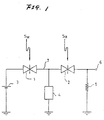
- Fig. 1 is a circuit diagram showing an embodiment of the present invention. Shown by 1 and 2 are photodetectors for write and read modes, respectively. Each of the photodetectors 1 and 2 comprises two spaced Schottky electrodes that are disposed to face each other on a semiconductor substrate in a symmetric way. These photodetectors operate so that they become conducting only when a predetermined amount of light is incident thereon. For details of the construction of these photodetectors 1 and 2, see "Metal-Semiconductor-Metal Photodetector for High-Speed Optoelectronic Circuits" by T. Sugeta, T. Urisu, S. Sakata and Y. Mizushima in Jpn. J. of Appl.
- One end of the photodetector 1 is connected to the positive electrode of a bias voltage source 3 having its negative electrode grounded.
- the other end of the photodetector 1 is connected to one end of the photodetector 2 via a signal conductor 7.
- a resetting switch 4 having one end grounded, is connected at the other end to the middle point of the signal conductor 7.
- the other end of the photodetector 2 is connected both to a load resistance 5, having one end grounded, and to an output terminal 6.
- each photodetector in the circuit comprises a pair of symmetric Schottky electrodes, which is operable at either polarity of electrical bias, the polarity of the output signal is selective based on the polarity of the photodetectors. Thus, the output polarity can be changed, if desired.
- the photodetector 1 As long as an optical write signal S W is incident on the photodetector 1, the latter remains conducting and the potential of the signal conductor 7 is raised to a level equal to the potential of the bias voltage source 3. Thereafter, in response to a decrease in the write signal S W , the photodetector 1 becomes non-conducting and the voltage at that time is held in the signal conductor 7. If, under this condition, an optical read signal S R is incident on the photodetector 2, the latter becomes conducting and a current flows through the load resistance 5, thereby producing a signal at the output terminal 6. No output signal will be produced unless a potential has built up in the signal conductor 7 when read signal S R is incident on the photodetector 2. Thus, in the circuit being described, the signal conductor 7 is normally held at high impedance or floating potential to realize a 1-bit memory circuit.
- the resetting switch 4 is an optional element and may be employed, for instance, to initialize the state of memory.
- a switching element incorporating a bias source may be used as the resetting switch 4 and specific examples of such element are a transistor that operates on a gate electric signal and a photodetector that operates on an optical signal.
- These switching elements may be replaced by a CR element having a large time constant. In this latter case, memory is held within an operating range effectively defined by the time constant.
- a potential storing function is realized by making the time constant of the signal conductor 7 substantially long, and in order to reset it at substantially long time constant, a transistor, etc. may be used.
- FIG. 2 is a perspective view showing an optical memory circuit device in which the circuit shown in Fig. 1 is actually integrated monolithically.
- a semiconductor substrate shown by reference numeral 11 is made of a semiconductor material such as Si or GaAs.
- the grounding conductor 10 taken together with the signal conductors 7 - 9 form a strip line.
- An insulating thin film is provided between the semiconductor substrate 11 and each of the signal conductors 7 - 9 and the grounding conductor 10 except in the areas where the photodetectors 1 and 2, resetting switch 4 and load resistance 5 are formed.
- the photodetector 1 is formed of two Schottky junctions between the edges of the signal conductors 7 and 8 and the semiconductor substrate 11.
- the photodetector 2 is formed of two Schottky junctions between the edges of the signal conductors 7 and 9 and the semiconductor substrate 11. In both cases, the surface of the semiconductor substrate between the two Schottky junctions serves as a light-receiving surface.
- the resetting switch 4 is also constructed as a photodetector having a similar design to the photodetectors 1 and 2, that is, two Schottky junctions are formed between the edges of the signal conductor 7 and grounding conductor 10 and the semiconductor substrate 11.
- the load resistance 5 is a n+ high-density-doped region formed by doping impurities in the surface region of the semiconductor substrate 11, and opposite ends of this resistance 5 are connected to the signal conductor 9 and the grounding conductor 10.
- the signal conductor 8 is connected to an external bias voltage source 3 whereas the signal conductor 9 is connected to the output terminal 6.
- the circuit system shown in Fig. 2 will operate as follows.
- an optical write signal S W is supplied to the photodetector 1
- a potential of the signal conductor 7 is raised to a level equal to the potential of the bias voltage source 3.
- the potential at that time is held in the signal conductor 7.
- an optical read signal S R is supplied to the photodetector 2
- a current flows through the load resistance 5 and a signal is produced at the output terminal 6.
- an optical reset signal S RT is incident on the photodetector 4 which is a resetting switch, the potential of the signal conductor 7 is erased to reset the overall circuit.
- photodetectors such as by forming a Schottky electrode by arranging two ohmic electrodes in a symmetric way.
- the load resistance 5 is formed by doping impurities into the semiconductor substrate. It should, however, be noted that this is not the only method of forming the load resistance 5 and that a film resistor may be employed.
- the photodetector 1 is connected to the positive electrode of the bias voltage source 3 but the device operation is in no way dependent upon the polarity of the bias voltage.
- the optical memory circuit of the present invention has the advantage that it is capable of performing a memory operation on optical input signals with a simple configuration in which two photodetectors are connected in series by an intermediate signal conductor which has a time constant of potential set to an appropriately large value.
- the optical memory circuit of the present invention which does not use any slow active devices such as a transistor is capable of very fast memory operation. This would be a great benefit to optical wiring which is becoming popular as a means for increasing the operating speed of computers, because, with this invention, data storage processing can be accomplished with the high-speed characteristic of light being utilized to the fullest extent.
Description
- The present invention relates to a memory circuit having the features of the generic clause of
Claim 1. Such a memory circuit is known from GB-A-2 185 165. - In general, conventional semiconductor memory circuits employ transistors in each of the writing, memory and reading sections. If it is necessary to design an optical memory circuit that performs a reading and a writing operation with an optical signal, common practice is to couple a photodetector to each of the read signal and write signal input terminals in a conventional memory circuit composed of transistors. A problem with this approach is that since the memory circuit section is of a conventional type which uses transistors, the writing and reading speed are limited by the operating time of the transistor, thus making it impossible to fully exploit the advantage of using input optical signals which permit high-speed operation.
- It is, therefore, the object of the present invention to provide an optical memory circuit using input optical signals which permits high-speed operation.
- This object is solved by an optical memory circuit having the features of
Claim 1. - Preferred embodiments are disclosed in the dependent Claims.
- When light is incident on one of the two photodetectors, carriers are activated by photoelectric conversion and charges are stored in the intermediate signal conductor. Those charges are held in the intermediate signal conductor until light is incident on the other photodetector, whereupon it becomes conducting and the stored charges are released.
- Other and further objects, features and advantages of the invention will appear more fully from the following description taken in connection with the accompanying drawings.
- Fig. 1 is a circuit diagram showing an embodiment of the present invention;
- Fig. 2 is a perspective view showing an integrated circuit device that incorporates the above embodiment of the present invention.
- Fig. 1 is a circuit diagram showing an embodiment of the present invention. Shown by 1 and 2 are photodetectors for write and read modes, respectively. Each of the
photodetectors photodetectors photodetectors photodetector 1 is connected to the positive electrode of abias voltage source 3 having its negative electrode grounded. The other end of thephotodetector 1 is connected to one end of thephotodetector 2 via asignal conductor 7. Aresetting switch 4, having one end grounded, is connected at the other end to the middle point of thesignal conductor 7. The other end of thephotodetector 2 is connected both to aload resistance 5, having one end grounded, and to anoutput terminal 6. - The circuit shown in Fig. 1 will operate as follows.
- Because each photodetector in the circuit comprises a pair of symmetric Schottky electrodes, which is operable at either polarity of electrical bias, the polarity of the output signal is selective based on the polarity of the photodetectors. Thus, the output polarity can be changed, if desired.
- As long as an optical write signal SW is incident on the
photodetector 1, the latter remains conducting and the potential of thesignal conductor 7 is raised to a level equal to the potential of thebias voltage source 3. Thereafter, in response to a decrease in the write signal SW, thephotodetector 1 becomes non-conducting and the voltage at that time is held in thesignal conductor 7. If, under this condition, an optical read signal SR is incident on thephotodetector 2, the latter becomes conducting and a current flows through theload resistance 5, thereby producing a signal at theoutput terminal 6. No output signal will be produced unless a potential has built up in thesignal conductor 7 when read signal SR is incident on thephotodetector 2. Thus, in the circuit being described, thesignal conductor 7 is normally held at high impedance or floating potential to realize a 1-bit memory circuit. - The resetting
switch 4 is an optional element and may be employed, for instance, to initialize the state of memory. If necessary, a switching element incorporating a bias source may be used as the resettingswitch 4 and specific examples of such element are a transistor that operates on a gate electric signal and a photodetector that operates on an optical signal. These switching elements may be replaced by a CR element having a large time constant. In this latter case, memory is held within an operating range effectively defined by the time constant. As described above, a potential storing function is realized by making the time constant of thesignal conductor 7 substantially long, and in order to reset it at substantially long time constant, a transistor, etc. may be used. - Fig. 2 is a perspective view showing an optical memory circuit device in which the circuit shown in Fig. 1 is actually integrated monolithically. In Fig. 2, the elements which are the same as those shown in Fig. 1 are identified by like numerals or symbols. A semiconductor substrate shown by
reference numeral 11 is made of a semiconductor material such as Si or GaAs. There are provided on the surface of the semiconductor substrate 11 aphotodetector 1 for write mode, aphotodetector 2 for read mode, aresetting switch 4, aload resistance 5, signal conductors 7 - 9, and agrounding conductor 10. Thegrounding conductor 10 taken together with the signal conductors 7 - 9 form a strip line. An insulating thin film is provided between thesemiconductor substrate 11 and each of the signal conductors 7 - 9 and thegrounding conductor 10 except in the areas where thephotodetectors switch 4 andload resistance 5 are formed. Thephotodetector 1 is formed of two Schottky junctions between the edges of thesignal conductors semiconductor substrate 11. Thephotodetector 2 is formed of two Schottky junctions between the edges of thesignal conductors semiconductor substrate 11. In both cases, the surface of the semiconductor substrate between the two Schottky junctions serves as a light-receiving surface. The resettingswitch 4 is also constructed as a photodetector having a similar design to thephotodetectors signal conductor 7 andgrounding conductor 10 and thesemiconductor substrate 11. Theload resistance 5 is a n⁺ high-density-doped region formed by doping impurities in the surface region of thesemiconductor substrate 11, and opposite ends of thisresistance 5 are connected to thesignal conductor 9 and thegrounding conductor 10. Thesignal conductor 8 is connected to an externalbias voltage source 3 whereas thesignal conductor 9 is connected to theoutput terminal 6. - The circuit system shown in Fig. 2 will operate as follows. When an optical write signal SW is supplied to the
photodetector 1, a potential of thesignal conductor 7 is raised to a level equal to the potential of thebias voltage source 3. In response to a decrease in the incident write signal SW the potential at that time is held in thesignal conductor 7. Thereafter, when an optical read signal SR is supplied to thephotodetector 2, a current flows through theload resistance 5 and a signal is produced at theoutput terminal 6. When an optical reset signal SRT is incident on thephotodetector 4 which is a resetting switch, the potential of thesignal conductor 7 is erased to reset the overall circuit. - Other designs may of course be employed to construct photodetectors, such as by forming a Schottky electrode by arranging two ohmic electrodes in a symmetric way.
- In the embodiment shown in Fig. 2, the
load resistance 5 is formed by doping impurities into the semiconductor substrate. It should, however, be noted that this is not the only method of forming theload resistance 5 and that a film resistor may be employed. In the embodiment shown in Fig. 1 and 2, thephotodetector 1 is connected to the positive electrode of thebias voltage source 3 but the device operation is in no way dependent upon the polarity of the bias voltage. - As will be understood from the foregoing description, the optical memory circuit of the present invention has the advantage that it is capable of performing a memory operation on optical input signals with a simple configuration in which two photodetectors are connected in series by an intermediate signal conductor which has a time constant of potential set to an appropriately large value. In addition, the optical memory circuit of the present invention which does not use any slow active devices such as a transistor is capable of very fast memory operation. This would be a great benefit to optical wiring which is becoming popular as a means for increasing the operating speed of computers, because, with this invention, data storage processing can be accomplished with the high-speed characteristic of light being utilized to the fullest extent.
Claims (5)
- An optical memory circuit comprising a semiconductor substrate (11), two photodetectors (1,2) formed symmetrically on said semiconductor substrate (11), an intermediate signal conductor (7) connecting said photodetectors, and a bias voltage means (3) connected to one of said photodetectors (1,2) for providing a bias voltage, said photodetectors (1,2) and said intermediate signal conductor (7) being connected in series in a closed circuit, and said intermediate signal conductor (7) being provided with a predetermined potential and having a capacitance with a predetermined time constant such that charges are stored in said intermediate signal conductor (7) when a light signal is incident on one of said photodetectors (1,2) and said stored charges are released from said intermediate signal conductor (7) when said light signal is incident on the other one of said photodetectors (1,2)
characterized in that
each of said two photodetectors (1,2) is operable at a bias of either polarity and comprises two Schottky diodes facing each other and said bias voltage means (3) provides a bias voltage of either polarity to said intermediate signal conductor (7) through one of said photodetectors (1,2). - The optical memory circuit of Claim 1
characterized in that
it comprises a resetting switch (4), connected to said intermediate signal conductor (7), for resetting said predetermined potential of said intermediate signal conductor (7). - The optical memory circuit of Claim 1 or 2
characterized in that
said two photodetectors (1,2) and said intermediate signal conductor (7) are formed monolithically on said semiconductor substrate (11). - The optical memory circuit of any of the Claims 1 to 3
characterized in that
a load resistance (5) is connected to one of said photodetectors (1,2) and is formed on said semiconductor substrate (11). - The optical memory circuit of any of the Claims 1 to 4
characterized in that
said optical memory circuit is in the form of a strip line.
Applications Claiming Priority (2)
| Application Number | Priority Date | Filing Date | Title |
|---|---|---|---|
| JP191385/88 | 1988-07-29 | ||
| JP63191385A JPH0240197A (en) | 1988-07-29 | 1988-07-29 | Optical memory circuit |
Publications (3)
| Publication Number | Publication Date |
|---|---|
| EP0352814A2 EP0352814A2 (en) | 1990-01-31 |
| EP0352814A3 EP0352814A3 (en) | 1990-12-19 |
| EP0352814B1 true EP0352814B1 (en) | 1993-12-29 |
Family
ID=16273719
Family Applications (1)
| Application Number | Title | Priority Date | Filing Date |
|---|---|---|---|
| EP89114010A Expired - Lifetime EP0352814B1 (en) | 1988-07-29 | 1989-07-28 | Optical memory circuit |
Country Status (4)
| Country | Link |
|---|---|
| US (1) | US5034921A (en) |
| EP (1) | EP0352814B1 (en) |
| JP (1) | JPH0240197A (en) |
| DE (1) | DE68911781T2 (en) |
Families Citing this family (2)
| Publication number | Priority date | Publication date | Assignee | Title |
|---|---|---|---|---|
| JPH04315896A (en) * | 1991-04-12 | 1992-11-06 | Takayama:Kk | Optical memory |
| WO2010039979A1 (en) * | 2008-10-01 | 2010-04-08 | Avedro, Inc. | Eye therapy system |
Family Cites Families (4)
| Publication number | Priority date | Publication date | Assignee | Title |
|---|---|---|---|---|
| US3196405A (en) * | 1961-12-18 | 1965-07-20 | Ibm | Variable capacitance information storage system |
| JPS4967532A (en) * | 1972-11-01 | 1974-07-01 | ||
| JPS54129838A (en) * | 1978-03-31 | 1979-10-08 | Toshirou Sasai | Mos memory circuit |
| GB8531347D0 (en) * | 1985-12-19 | 1986-01-29 | Goran K | Optoelectronic dynamic memory device |
-
1988
- 1988-07-29 JP JP63191385A patent/JPH0240197A/en active Granted
-
1989
- 1989-07-06 US US07/375,983 patent/US5034921A/en not_active Expired - Fee Related
- 1989-07-28 DE DE89114010T patent/DE68911781T2/en not_active Expired - Fee Related
- 1989-07-28 EP EP89114010A patent/EP0352814B1/en not_active Expired - Lifetime
Also Published As
| Publication number | Publication date |
|---|---|
| DE68911781T2 (en) | 1994-04-14 |
| JPH0240197A (en) | 1990-02-08 |
| US5034921A (en) | 1991-07-23 |
| EP0352814A2 (en) | 1990-01-31 |
| DE68911781D1 (en) | 1994-02-10 |
| EP0352814A3 (en) | 1990-12-19 |
| JPH0444839B2 (en) | 1992-07-22 |
Similar Documents
| Publication | Publication Date | Title |
|---|---|---|
| US4399372A (en) | Integrated circuit having spare parts activated by a high-to-low adjustable resistance device | |
| FR2536607A1 (en) | INTERFACE CIRCUIT | |
| US4029971A (en) | Tri-state logic circuit | |
| US7411172B1 (en) | Method and apparatus for resetting a high speed latch circuit | |
| EP0347935A3 (en) | Semiconductor memory device | |
| CA1235504A (en) | Data storage element having input and output ports isolated from regenerative circuit | |
| EP0352814B1 (en) | Optical memory circuit | |
| US4999688A (en) | Optical logic element with short switching time | |
| TW326535B (en) | Semiconductor memory device and read-out circuit | |
| US3900716A (en) | Optical static card reader | |
| GB1292355A (en) | Digital data storage circuits using transistors | |
| EP0289420B1 (en) | Semiconductor memory device using resonant-tunneling transistor | |
| US5572255A (en) | Image reading apparatus and method for driving appropriate photoelectric energy converting elements when first and second driving voltages are applied simultaneously | |
| KR0142340B1 (en) | Esd protection circuit employing channel depletion | |
| US4573079A (en) | Sensor array driving circuit | |
| US3868718A (en) | Field effect transistor having a pair of gate regions | |
| US3619665A (en) | Optically settable flip-flop | |
| JPS60254991A (en) | Time-division optical exchange | |
| EP0939933A1 (en) | Light detection device | |
| JP2738656B2 (en) | Optical receiver and method for initializing optical receiver | |
| US5477483A (en) | Memory device | |
| RU2075786C1 (en) | Memory gate | |
| JP2690554B2 (en) | Semiconductor memory device | |
| SU1064318A1 (en) | Storage element for random-access memory | |
| JPH05259522A (en) | Superconducting photoelectric signal conversion circuit |
Legal Events
| Date | Code | Title | Description |
|---|---|---|---|
| PUAI | Public reference made under article 153(3) epc to a published international application that has entered the european phase |
Free format text: ORIGINAL CODE: 0009012 |
|
| AK | Designated contracting states |
Kind code of ref document: A2 Designated state(s): DE GB |
|
| 17P | Request for examination filed |
Effective date: 19900705 |
|
| PUAL | Search report despatched |
Free format text: ORIGINAL CODE: 0009013 |
|
| AK | Designated contracting states |
Kind code of ref document: A3 Designated state(s): DE GB |
|
| RHK1 | Main classification (correction) |
Ipc: G11C 11/36 |
|
| 17Q | First examination report despatched |
Effective date: 19930217 |
|
| GRAA | (expected) grant |
Free format text: ORIGINAL CODE: 0009210 |
|
| AK | Designated contracting states |
Kind code of ref document: B1 Designated state(s): DE GB |
|
| REF | Corresponds to: |
Ref document number: 68911781 Country of ref document: DE Date of ref document: 19940210 |
|
| PLBE | No opposition filed within time limit |
Free format text: ORIGINAL CODE: 0009261 |
|
| STAA | Information on the status of an ep patent application or granted ep patent |
Free format text: STATUS: NO OPPOSITION FILED WITHIN TIME LIMIT |
|
| 26N | No opposition filed | ||
| PGFP | Annual fee paid to national office [announced via postgrant information from national office to epo] |
Ref country code: DE Payment date: 20010723 Year of fee payment: 13 |
|
| REG | Reference to a national code |
Ref country code: GB Ref legal event code: IF02 |
|
| PGFP | Annual fee paid to national office [announced via postgrant information from national office to epo] |
Ref country code: GB Payment date: 20020724 Year of fee payment: 14 |
|
| PG25 | Lapsed in a contracting state [announced via postgrant information from national office to epo] |
Ref country code: DE Free format text: LAPSE BECAUSE OF NON-PAYMENT OF DUE FEES Effective date: 20030201 |
|
| PG25 | Lapsed in a contracting state [announced via postgrant information from national office to epo] |
Ref country code: GB Free format text: LAPSE BECAUSE OF NON-PAYMENT OF DUE FEES Effective date: 20030728 |
|
| GBPC | Gb: european patent ceased through non-payment of renewal fee |
Effective date: 20030728 |