EP0352524A2 - Amplificateur de détection basse tension pour EPROM - Google Patents
Amplificateur de détection basse tension pour EPROM Download PDFInfo
- Publication number
- EP0352524A2 EP0352524A2 EP89112351A EP89112351A EP0352524A2 EP 0352524 A2 EP0352524 A2 EP 0352524A2 EP 89112351 A EP89112351 A EP 89112351A EP 89112351 A EP89112351 A EP 89112351A EP 0352524 A2 EP0352524 A2 EP 0352524A2
- Authority
- EP
- European Patent Office
- Prior art keywords
- inverter
- voltage
- transistor
- low
- low voltage
- Prior art date
- Legal status (The legal status is an assumption and is not a legal conclusion. Google has not performed a legal analysis and makes no representation as to the accuracy of the status listed.)
- Granted
Links
Images
Classifications
-
- G—PHYSICS
- G11—INFORMATION STORAGE
- G11C—STATIC STORES
- G11C16/00—Erasable programmable read-only memories
- G11C16/02—Erasable programmable read-only memories electrically programmable
- G11C16/06—Auxiliary circuits, e.g. for writing into memory
- G11C16/26—Sensing or reading circuits; Data output circuits
-
- G—PHYSICS
- G11—INFORMATION STORAGE
- G11C—STATIC STORES
- G11C7/00—Arrangements for writing information into, or reading information out from, a digital store
- G11C7/06—Sense amplifiers; Associated circuits, e.g. timing or triggering circuits
- G11C7/067—Single-ended amplifiers
Definitions
- the invention relates to a low voltage sense amplifier for an EPROM memory transistor.
- a sense amplifier is coupled to each column.
- the drains of the EPROM, transistors, which are connected to the column line, are coupled to the input of the respective sense amplifier.
- the column and the input of the sense amplifier are precharged to the main supply voltage VDD.
- VDD is typically about 5 volts but in some applications can reach 6 to 8 volts. Precharging the columns to such high voltages can cause some deprogramming of the memory transistors.
- This invention seeks to provide a low voltage sense amplifier for an EPROM memory transistor which can operate over a wide range of supply voltage and in which the above mentioned problem is solved.
- a low voltage sense amplifier for an EPROM memory transistor comprising a low voltage inverter having an input selectively couplable to the EPROM memory transistor, and an output; means for applying a selectable reference voltage as a supply voltage for the inverter and means responsive to a precharge signal for coupling the selectable reference voltage, as a precharge voltage, to the input of the low voltage inverter.
- the means for applying a selectable reference voltage as a supply voltage for the low voltage inverter may comprise a first MOS transistor coupled between a first power supply terminal and a supply line for the inverter, the first MOS transistor having a control electrode for receiving a selectable reference voltage.
- the means for coupling the selectable reference voltage as a precharge voltage to the input of the low voltage inverter may comprise a second MOS transistor, coupled between the supply line for the low voltage inverter and the input of the low voltage inverter, and having a control electrode for receiving said precharge signal.
- a resistive holding transistor is preferably connected across the second MOS transistor, the holding transistor having a control electrode coupled to be responsive to the output state of the low voltage inverter.
- a third MOS transistor may be connected across the said first MOS transistor, the third MOS transistor having a control electrode for receiving a signal indicative of a low supply voltage level of the first power supply, thereby to short circuit the first MOS transistor and couple the first power supply terminal directly to the supply line of the low voltage inverter.
- a low-to-high voltage inverter may be provided, coupled to the first power supply terminal and having a low voltage input coupled to the output of the low voltage inverter and having a high voltage output.
- an MOS transistor may be coupled between the low voltage input and a reference terminal, the transistor having a control electrode coupled to receive the precharge signal.
- a resistive holding transistor may be coupled between the output of the low-to-high voltage inverter and the first power supply terminal, the transistor having a control electrode coupled to the output of the high voltage inverter via a further inverter.
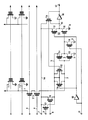
- EPROM memory transistors T1 and T2 have their drain electrodes coupled to column line 1 which is coupled via column select transistors TT3 to the input node 2 of a low voltage inverter 3.
- the column select transistors have their gate electrodes coupled to column select lines 4.
- the low voltage inverter is a CMOS inverter formed by series connected p and n-channel MOS transistors T4 and T5 respectively, which are coupled in series between a supply line 5 for the inverter and a ground reference terminal 6.
- Power supply for the supply line 5 is derived from an n-channel MOS transistor T6 coupled between a first power supply terminal 7 and the supply line 5.
- the terminal 7 receives a supply voltage VDD which is typically 5 volts but which may, depending upon application, lie between about 2v and about 8v.
- the gate electrode of the transistor T6 is coupled to a terminal 8 for receiving a selectable reference voltage VREF.
- a p-channel MOS transistor T7 is connected across the transistor T6 and has its gate electrode connected to a terminal 9 for receiving a low supply voltage signal VLOWN.
- a p-channel MOS transistor T8 is coupled between the supply line 5 and the input node 2 of the low voltage inverter 3.
- the gate control electrode of the transistor T8 is coupled via an inverter 10 to a terminal 11 for receiving a precharge select logic signal.
- the output of the low voltage inverter 3 is coupled to input node 12 of a low-to-high voltage inverter 13.
- the inverter 13 is formed by a switching n-channel MOS transistor T10 and a p-channel resistive holding transistor T9 which are connected in series between a supply line 14, connected to the power supply terminal 7, and ground reference terminal 6.
- the gate electrode of the transistor T10 is coupled to the input node 12 of the inverter 13.
- An n-channel MOS transistor T11 is coupled between the input node 12 and ground reference potential and has a gate electrode coupled to the precharge signal terminal 11.
- the inverter 13 has an output node 15 which is coupled via an inverter 16 to a final output terminal 17.
- a resistive pull-up p-channel MOS transistor T12 is coupled between the supply line 5 of the low voltage inverter 13 and the input node 2 of the inverter.
- the gate electrode of the resistive pull-up transistor T12 is coupled to that of the transistor T9 and to the output terminal 17.
- the resistive pull-up transistor 12 is formed in the same semiconductor n-tub as the p-channel transistors T8 and T4 and the substrates of these three transistors are common and are coupled to the supply line 5.
- a p-channel transistor T13 is connected in parallel with the resistive holding transistor T9 and has its gate electrode coupled via the inverter 10 to the precharge logic signal input terminal 11.
- EPROM sense amplifiers although nominally designed to operate with a 5 volt VDD supply voltage must be capable of handling a supply voltage which can lie vary, typically between 2 and 8 volts.
- the sense amplifier is formed from a low voltage inverter which receives as its supply voltage a selectable low reference voltage which is also fed as a precharge voltage to the input node of the low voltage inverter and to the columns of the EPROM memory.
- a supply VDD typically 5v, but possibly lying between about 2 and 8v, is applied to the terminal 7 and a reference voltage VREF is applied to the terminal 8 and hence to the gate electrode of the transistor T6.
- a low supply voltage detection circuit senses the supply voltage VDD and provides a signal VLOWN to the terminal 9, which signal is low when the supply voltage is low (typically 3 to 4.5 volts) and high at high voltages.
- VTN is the threshold voltage of an n-channel MOS transistor of the circuit
- PCV reference supply voltage
- the low voltage inverter 3 which is coupled to read the EPROM memory bit, is operated by a low voltage of typically less than 3v. This permits operation of the EPROM at very low supply voltage (below 2v).
- the column line 1 is selected by the application of VDD to the gates of the column select transistor TT3 and the input node 2 of the low voltage inverter is first precharged to a precharge voltage.
- the precharge logic signal PCH applied to terminal 1 goes high and the gate of the p-channel transistor T8 will go low by virtue of the inverter 10. Consequently the transistor T8 will turn on and apply the reference supply voltage PCV to the input node 2 of the low voltage inverter 3.
- the same precharge voltage is applied to the column 1 of the EPROM memory by a similar arrangement (not shown).
- the low voltage inverter 3 has a relatively long reaction time and thus to speed up the switching of the transistor T10 of the low-to-high voltage inverter 13, the transistor T11 is provided.
- the gate of the transistor T11 will go high and the transistor T11 will conduct and rapidly switch low the gate of the transistor T10 causing the inverter 13 to change states.
- the gate of T9 which is connected to receive the inverted precharge logic signal via the inverter 10, will go low causing the transistor T13 to turn on and to precharge the output node 15 of the inverter 13 to VDD.
- the low-to-high voltage inverter provides the required voltage level conversion from the low voltage of the bit sensing low voltage inverter 3, to the output level required by circuits (typically an MPU) coupled to the output terminal 17 of the sense amplifier.
- the inverter 13 On switching of the inverter 13, its output node 15 will go high and the final output terminal 17 will be low.
- the resistive holding transistors T12 and T9 will both be turned on and maintain the precharge voltage level after the precharge signal PCH is removed.
- one EPROM bit is selected by means of a gate select signal at the VDD supply voltage, which is applied to the gate of the selected EPROM transistor.
- the column line 1 either will, or will not draw any current.
- the precharge level at the input node 2, of the low voltage inverter 3 will be maintained and the output terminal 17 will stay low. If current is drawn the input node 2 of the inverter 3 will be discharged below its trigger point, in spite of the presence of the holding transistor T12. The low voltage inverter 3 will change states, which will also cause the switching of the low-to-high voltage inverter 13 by turning on the transistor T10. The output terminal 17 will thus be switched to the level of VDD, the supply voltage for the inverter 13.
- the sense amplifier described has the advantage that the drain precharge voltage can be very tightly controlled (in the example given, below 2v) and deprogramming during precharge is avoided. DC power consumption is totally avoided and also at the low precharge voltage used, the sense amplifier is faster than any known sense amplifier which draws no DC current.
- EPROM read operation is possible at very low supply voltage (below 2v).
Landscapes
- Read Only Memory (AREA)
Applications Claiming Priority (2)
| Application Number | Priority Date | Filing Date | Title |
|---|---|---|---|
| GB8817608A GB2221111B (en) | 1988-07-23 | 1988-07-23 | Eprom low voltage sense amplifier |
| GB8817608 | 1988-07-23 |
Publications (3)
| Publication Number | Publication Date |
|---|---|
| EP0352524A2 true EP0352524A2 (fr) | 1990-01-31 |
| EP0352524A3 EP0352524A3 (fr) | 1992-03-04 |
| EP0352524B1 EP0352524B1 (fr) | 1997-10-08 |
Family
ID=10641010
Family Applications (1)
| Application Number | Title | Priority Date | Filing Date |
|---|---|---|---|
| EP89112351A Expired - Lifetime EP0352524B1 (fr) | 1988-07-23 | 1989-07-06 | Amplificateur de détection basse tension pour EPROM |
Country Status (6)
| Country | Link |
|---|---|
| US (1) | US4965473A (fr) |
| EP (1) | EP0352524B1 (fr) |
| DE (1) | DE68928371T2 (fr) |
| GB (1) | GB2221111B (fr) |
| HK (1) | HK107095A (fr) |
| SG (1) | SG26410G (fr) |
Cited By (1)
| Publication number | Priority date | Publication date | Assignee | Title |
|---|---|---|---|---|
| EP0936621A1 (fr) * | 1998-02-13 | 1999-08-18 | STMicroelectronics S.r.l. | Amplficateur de détection améliorée pour mémoire non volatile avec plage de tensions d'alimentation étendue |
Families Citing this family (2)
| Publication number | Priority date | Publication date | Assignee | Title |
|---|---|---|---|---|
| US5729493A (en) * | 1996-08-23 | 1998-03-17 | Motorola Inc. | Memory suitable for operation at low power supply voltages and sense amplifier therefor |
| US8283198B2 (en) | 2010-05-10 | 2012-10-09 | Micron Technology, Inc. | Resistive memory and methods of processing resistive memory |
Citations (1)
| Publication number | Priority date | Publication date | Assignee | Title |
|---|---|---|---|---|
| EP0238812A2 (fr) * | 1986-02-24 | 1987-09-30 | Kabushiki Kaisha Toshiba | Circuit amplificateur de détection pour mémoire à semi-conducteurs |
Family Cites Families (1)
| Publication number | Priority date | Publication date | Assignee | Title |
|---|---|---|---|---|
| US4837465A (en) * | 1985-01-16 | 1989-06-06 | Digital Equipment Corp | Single rail CMOS register array and sense amplifier circuit therefor |
-
1988
- 1988-07-23 GB GB8817608A patent/GB2221111B/en not_active Expired - Fee Related
- 1988-07-23 SG SG1995907150A patent/SG26410G/en unknown
-
1989
- 1989-07-06 EP EP89112351A patent/EP0352524B1/fr not_active Expired - Lifetime
- 1989-07-06 DE DE68928371T patent/DE68928371T2/de not_active Expired - Fee Related
- 1989-07-18 US US07/381,354 patent/US4965473A/en not_active Expired - Lifetime
-
1995
- 1995-06-29 HK HK107095A patent/HK107095A/xx not_active IP Right Cessation
Patent Citations (1)
| Publication number | Priority date | Publication date | Assignee | Title |
|---|---|---|---|---|
| EP0238812A2 (fr) * | 1986-02-24 | 1987-09-30 | Kabushiki Kaisha Toshiba | Circuit amplificateur de détection pour mémoire à semi-conducteurs |
Non-Patent Citations (1)
| Title |
|---|
| IEEE JOURNAL OF SOLID-STATE CIRCUITS. vol. SC-20, no. 5, October 1985, NEW YORK US pages 971 - 978; R.D.JOLLY ET AL.: 'A 53-ns 64K EEPROM' * |
Cited By (2)
| Publication number | Priority date | Publication date | Assignee | Title |
|---|---|---|---|---|
| EP0936621A1 (fr) * | 1998-02-13 | 1999-08-18 | STMicroelectronics S.r.l. | Amplficateur de détection améliorée pour mémoire non volatile avec plage de tensions d'alimentation étendue |
| US6650147B2 (en) | 1998-02-13 | 2003-11-18 | Stmicroelectronics S.R.L. | Sense amplifier with extended supply voltage range |
Also Published As
| Publication number | Publication date |
|---|---|
| DE68928371D1 (de) | 1997-11-13 |
| GB8817608D0 (en) | 1988-09-01 |
| HK107095A (en) | 1995-07-07 |
| EP0352524A3 (fr) | 1992-03-04 |
| DE68928371T2 (de) | 1998-04-09 |
| GB2221111B (en) | 1993-01-06 |
| US4965473A (en) | 1990-10-23 |
| SG26410G (en) | 1995-09-01 |
| EP0352524B1 (fr) | 1997-10-08 |
| GB2221111A (en) | 1990-01-24 |
Similar Documents
| Publication | Publication Date | Title |
|---|---|---|
| US4389705A (en) | Semiconductor memory circuit with depletion data transfer transistor | |
| US5187392A (en) | Programmable logic device with limited signal swing | |
| CA2033020C (fr) | Amplificateur de detection differentiel c-mos | |
| US6442090B1 (en) | Differential sensing amplifier for content addressable memory | |
| US6301180B1 (en) | Sense amplifier circuit and semiconductor storage device | |
| KR100266633B1 (ko) | 레벨 쉬프터 회로 | |
| KR0146387B1 (ko) | 플립플롭형 증폭 회로 | |
| KR100548558B1 (ko) | 반도체 장치용 내부전압 발생기 | |
| KR930007278B1 (ko) | 반도체 메모리용 센스회로 | |
| KR100215165B1 (ko) | 집적회로 | |
| JP2851035B2 (ja) | プログラム可能な論理装置 | |
| US5272674A (en) | High speed memory sense amplifier with noise reduction | |
| KR910013279A (ko) | 감지 증폭기 및 이에 의한 방법 | |
| KR100567497B1 (ko) | 버스 인터페이스 회로 및 리시버 회로 | |
| KR100195975B1 (ko) | 출력버퍼 | |
| US6590420B1 (en) | Level shifting circuit and method | |
| EP0063357A2 (fr) | Circuit d'attaque | |
| EP0352524B1 (fr) | Amplificateur de détection basse tension pour EPROM | |
| JPH0793026B2 (ja) | デコーダ回路 | |
| US6195297B1 (en) | Semiconductor memory device having pull-down function for non-selected bit lines | |
| US6314041B1 (en) | Memory with a reduced leakage current | |
| KR930008413B1 (ko) | 반도체기억장치 | |
| GB2201059A (en) | High voltage FET circuit | |
| US4060740A (en) | Sensing amplifier for capacitive MISFET memory | |
| US4857767A (en) | High-density low-power circuit for sustaining a precharge level |
Legal Events
| Date | Code | Title | Description |
|---|---|---|---|
| PUAI | Public reference made under article 153(3) epc to a published international application that has entered the european phase |
Free format text: ORIGINAL CODE: 0009012 |
|
| AK | Designated contracting states |
Kind code of ref document: A2 Designated state(s): DE FR IT |
|
| PUAL | Search report despatched |
Free format text: ORIGINAL CODE: 0009013 |
|
| AK | Designated contracting states |
Kind code of ref document: A3 Designated state(s): DE FR IT |
|
| 17P | Request for examination filed |
Effective date: 19920827 |
|
| 17Q | First examination report despatched |
Effective date: 19930420 |
|
| GRAH | Despatch of communication of intention to grant a patent |
Free format text: ORIGINAL CODE: EPIDOS IGRA |
|
| GRAH | Despatch of communication of intention to grant a patent |
Free format text: ORIGINAL CODE: EPIDOS IGRA |
|
| GRAH | Despatch of communication of intention to grant a patent |
Free format text: ORIGINAL CODE: EPIDOS IGRA |
|
| ITF | It: translation for a ep patent filed |
Owner name: BARZANO' E ZANARDO ROMA S.P.A. |
|
| GRAA | (expected) grant |
Free format text: ORIGINAL CODE: 0009210 |
|
| AK | Designated contracting states |
Kind code of ref document: B1 Designated state(s): DE FR IT |
|
| REF | Corresponds to: |
Ref document number: 68928371 Country of ref document: DE Date of ref document: 19971113 |
|
| ET | Fr: translation filed | ||
| PLBE | No opposition filed within time limit |
Free format text: ORIGINAL CODE: 0009261 |
|
| STAA | Information on the status of an ep patent application or granted ep patent |
Free format text: STATUS: NO OPPOSITION FILED WITHIN TIME LIMIT |
|
| 26N | No opposition filed | ||
| PG25 | Lapsed in a contracting state [announced via postgrant information from national office to epo] |
Ref country code: IT Free format text: LAPSE BECAUSE OF NON-PAYMENT OF DUE FEES;WARNING: LAPSES OF ITALIAN PATENTS WITH EFFECTIVE DATE BEFORE 2007 MAY HAVE OCCURRED AT ANY TIME BEFORE 2007. THE CORRECT EFFECTIVE DATE MAY BE DIFFERENT FROM THE ONE RECORDED. Effective date: 20050706 |
|
| PGFP | Annual fee paid to national office [announced via postgrant information from national office to epo] |
Ref country code: FR Payment date: 20060705 Year of fee payment: 18 |
|
| PGFP | Annual fee paid to national office [announced via postgrant information from national office to epo] |
Ref country code: DE Payment date: 20060731 Year of fee payment: 18 |
|
| PG25 | Lapsed in a contracting state [announced via postgrant information from national office to epo] |
Ref country code: DE Free format text: LAPSE BECAUSE OF NON-PAYMENT OF DUE FEES Effective date: 20080201 |
|
| REG | Reference to a national code |
Ref country code: FR Ref legal event code: ST Effective date: 20080331 |
|
| PG25 | Lapsed in a contracting state [announced via postgrant information from national office to epo] |
Ref country code: FR Free format text: LAPSE BECAUSE OF NON-PAYMENT OF DUE FEES Effective date: 20070731 |