EP0351144B1 - Power supplies - Google Patents
Power supplies Download PDFInfo
- Publication number
- EP0351144B1 EP0351144B1 EP89306905A EP89306905A EP0351144B1 EP 0351144 B1 EP0351144 B1 EP 0351144B1 EP 89306905 A EP89306905 A EP 89306905A EP 89306905 A EP89306905 A EP 89306905A EP 0351144 B1 EP0351144 B1 EP 0351144B1
- Authority
- EP
- European Patent Office
- Prior art keywords
- rectifier
- inductor
- current
- circuit
- output
- Prior art date
- Legal status (The legal status is an assumption and is not a legal conclusion. Google has not performed a legal analysis and makes no representation as to the accuracy of the status listed.)
- Expired - Lifetime
Links
Images


Classifications
-
- H—ELECTRICITY
- H02—GENERATION; CONVERSION OR DISTRIBUTION OF ELECTRIC POWER
- H02M—APPARATUS FOR CONVERSION BETWEEN AC AND AC, BETWEEN AC AND DC, OR BETWEEN DC AND DC, AND FOR USE WITH MAINS OR SIMILAR POWER SUPPLY SYSTEMS; CONVERSION OF DC OR AC INPUT POWER INTO SURGE OUTPUT POWER; CONTROL OR REGULATION THEREOF
- H02M1/00—Details of apparatus for conversion
- H02M1/40—Means for preventing magnetic saturation
-
- H—ELECTRICITY
- H02—GENERATION; CONVERSION OR DISTRIBUTION OF ELECTRIC POWER
- H02M—APPARATUS FOR CONVERSION BETWEEN AC AND AC, BETWEEN AC AND DC, OR BETWEEN DC AND DC, AND FOR USE WITH MAINS OR SIMILAR POWER SUPPLY SYSTEMS; CONVERSION OF DC OR AC INPUT POWER INTO SURGE OUTPUT POWER; CONTROL OR REGULATION THEREOF
- H02M1/00—Details of apparatus for conversion
- H02M1/32—Means for protecting converters other than automatic disconnection
- H02M1/34—Snubber circuits
-
- H—ELECTRICITY
- H02—GENERATION; CONVERSION OR DISTRIBUTION OF ELECTRIC POWER
- H02M—APPARATUS FOR CONVERSION BETWEEN AC AND AC, BETWEEN AC AND DC, OR BETWEEN DC AND DC, AND FOR USE WITH MAINS OR SIMILAR POWER SUPPLY SYSTEMS; CONVERSION OF DC OR AC INPUT POWER INTO SURGE OUTPUT POWER; CONTROL OR REGULATION THEREOF
- H02M1/00—Details of apparatus for conversion
- H02M1/08—Circuits specially adapted for the generation of control voltages for semiconductor devices incorporated in static converters
-
- H—ELECTRICITY
- H02—GENERATION; CONVERSION OR DISTRIBUTION OF ELECTRIC POWER
- H02M—APPARATUS FOR CONVERSION BETWEEN AC AND AC, BETWEEN AC AND DC, OR BETWEEN DC AND DC, AND FOR USE WITH MAINS OR SIMILAR POWER SUPPLY SYSTEMS; CONVERSION OF DC OR AC INPUT POWER INTO SURGE OUTPUT POWER; CONTROL OR REGULATION THEREOF
- H02M3/00—Conversion of dc power input into dc power output
- H02M3/02—Conversion of dc power input into dc power output without intermediate conversion into ac
- H02M3/04—Conversion of dc power input into dc power output without intermediate conversion into ac by static converters
- H02M3/10—Conversion of dc power input into dc power output without intermediate conversion into ac by static converters using discharge tubes with control electrode or semiconductor devices with control electrode
- H02M3/145—Conversion of dc power input into dc power output without intermediate conversion into ac by static converters using discharge tubes with control electrode or semiconductor devices with control electrode using devices of a triode or transistor type requiring continuous application of a control signal
- H02M3/155—Conversion of dc power input into dc power output without intermediate conversion into ac by static converters using discharge tubes with control electrode or semiconductor devices with control electrode using devices of a triode or transistor type requiring continuous application of a control signal using semiconductor devices only
-
- H—ELECTRICITY
- H03—ELECTRONIC CIRCUITRY
- H03K—PULSE TECHNIQUE
- H03K17/00—Electronic switching or gating, i.e. not by contact-making and –breaking
- H03K17/08—Modifications for protecting switching circuit against overcurrent or overvoltage
- H03K17/081—Modifications for protecting switching circuit against overcurrent or overvoltage without feedback from the output circuit to the control circuit
- H03K17/0814—Modifications for protecting switching circuit against overcurrent or overvoltage without feedback from the output circuit to the control circuit by measures taken in the output circuit
- H03K17/08142—Modifications for protecting switching circuit against overcurrent or overvoltage without feedback from the output circuit to the control circuit by measures taken in the output circuit in field-effect transistor switches
-
- H—ELECTRICITY
- H02—GENERATION; CONVERSION OR DISTRIBUTION OF ELECTRIC POWER
- H02M—APPARATUS FOR CONVERSION BETWEEN AC AND AC, BETWEEN AC AND DC, OR BETWEEN DC AND DC, AND FOR USE WITH MAINS OR SIMILAR POWER SUPPLY SYSTEMS; CONVERSION OF DC OR AC INPUT POWER INTO SURGE OUTPUT POWER; CONTROL OR REGULATION THEREOF
- H02M1/00—Details of apparatus for conversion
- H02M1/32—Means for protecting converters other than automatic disconnection
- H02M1/34—Snubber circuits
- H02M1/346—Passive non-dissipative snubbers
-
- Y—GENERAL TAGGING OF NEW TECHNOLOGICAL DEVELOPMENTS; GENERAL TAGGING OF CROSS-SECTIONAL TECHNOLOGIES SPANNING OVER SEVERAL SECTIONS OF THE IPC; TECHNICAL SUBJECTS COVERED BY FORMER USPC CROSS-REFERENCE ART COLLECTIONS [XRACs] AND DIGESTS
- Y02—TECHNOLOGIES OR APPLICATIONS FOR MITIGATION OR ADAPTATION AGAINST CLIMATE CHANGE
- Y02B—CLIMATE CHANGE MITIGATION TECHNOLOGIES RELATED TO BUILDINGS, e.g. HOUSING, HOUSE APPLIANCES OR RELATED END-USER APPLICATIONS
- Y02B70/00—Technologies for an efficient end-user side electric power management and consumption
- Y02B70/10—Technologies improving the efficiency by using switched-mode power supplies [SMPS], i.e. efficient power electronics conversion e.g. power factor correction or reduction of losses in power supplies or efficient standby modes
Definitions
- This invention relates to improvements in power supplies.
- the invention relates to an improved rectifier circuit for use in power supplies, e.g. boost convertor power supplies.
- Boost convertor circuits have an electronic switch controlling the current through an inductor. When the current is switched off, a high voltage is created across the inductor which passes through a rectifier to charge a capacitor to a higher voltage than the original supply voltage.
- T. Yamada et al A New Noise Suppression with Amorphous Saturable Reactor", IEEE APEC Proceeding April 1986, PR 134-140 has proposed a circuit the purpose of which was to suppress output switching noise due to diode reverse current in switching power supply output rectifiers.
- the circuit was applied to a boost convertor as shown in Figure 5 by T. Ninomiya et al, see “Noise Suppression by Magnetic Snubber in Switching Power Convertors", IEEE PESC Record April 1988 IP 1133-1140.
- An inductor puts a reverse voltage across the reactor to restore its flux density. Unfortunately, however this also puts a high surge reverse voltage across the diode. When the switch turns off, the reactor is not totally saturated and a high surge voltage appears across the switch.
- the invention has therefore been made with these points in mind and aims to provide a more efficient rectifier circuit.
- a rectifier circuit comprising a rectifier intended to allow current to flow in a forward direction to an output, a saturable inductor connected in series with the rectifier allowing the ready passage of current in the forward direction but blocking reverse recovery rectifier current, the saturable inductor being connected in parallel with a rectifier in series with inductor means through which reverse recovery rectifier current passes and for limiting that reverse recovery current, energy stored in those inductor means being used to re-set the saturable inductor to its saturation state for a subsequent flow of current in the forward direction, and is characterised in that capacitor means are connected across the inductor means for absorbing surplus energy from the inductor means, and rectifier means are connected between the capacitor means and the output for guiding that surplus energy to the output.
- additional capacitor means are provided across the rectifier to aid in re-setting of the saturable inductor to its saturation state, and/or to slow down the application of reverse potential across the rectifier. This further reduces reverse recovery rectifier current.
- the rectifier circuit will normally guide a flow of AC power to provide a DC output, and the source of that AC power can be a transformer. More than one rectifier circuit according to the invention can be provided to give a half- or full-wave DC output. Also a further inductor may be employed to smooth the flow of power from the source to the output.
- the rectifier circuit is used as part of a convertor.
- a convertor may comprise a first inductor means to store energy which is repeatedly switched by an electronic switch, the switching controlling the energy stored in the inductor means to be delivered to the output through a rectifier circuit according to the invention.
- additional rectifier means are provided to clamp the voltage across the electronic switch to the output voltage as a maximum, so reducing the maximum stress on the electronic switch.
- current limiting means such as another inductor are desirably provided in series with the switch to limit the initial current when it turns on so that the voltage across it has time to fall from the higher output voltage to the input voltage before it passes a high current.
- the energy in this additional inductor when the electronic switch becomes non-conducting is then desirably dissipated through the additional rectifier means for use together with the output potential so that it need not be wasted.
- the invention is applicable to boost convertors where an inductor is provided in series with the rectifier circuit to charge an output capacitor, the inductor current being switched between on and off, e.g. between ground and the output, at high frequency by an electronic switch such as a field effect transistor.
- the invention is, however, also applicable to all forms of power convertor employing a transformer for isolation, e.g. where the electronic switch is in series with an inductor, such as a buck convertor, a circuit where the inductor is itself the load, e.g. an inductive motor, in a half or full bridge rectifier arrangement, a forward convertor, or a flyback convertor.
- the boost convertor circuit 10 shown in Figure 1 includes a boost inductor L1 in the line between the input voltage V IN and output boosted voltage V OUT .
- An electronic switch Q1 such as a field effect transistor (FET) is positioned between the output side of the inductor L1 and ground.
- FET field effect transistor
- the switch Q1 is rapidly oscillated between being switched on and switched off. When it is on, ie. conducting, current passes through the inductor L1 to ground. When it switches off, this current is interrupted and this interruption creates a higher potential in the inductor L1.
- a diode D4 is in series with the inductor L1 before a capacitor C4.
- the diode D4 prevent return loss of the charge stored in the capacitor C4.
- the switch Q1 is controlled in a conventional manner by a pulse width modulated control IC12, eg. Unitrode UC1842, which monitors and regulates the output voltage by driving switch Q1 at the correct duty cycle depending upon input voltage and output power.
- a pulse width modulated control IC12 eg. Unitrode UC1842
- a known problem with this basic boost circuit 10 is the finite time required for recombination of charges in the diode D4. Thus until these recombine, a reverse recovery current is possible. Therefore, a negative spike of reverse current can pass each time the switch Q1 switches off. Attempts to prevent this reverse current have not been particularly successful.
- a small inductor L3 may be provided between the inductor L1 and diode D4.
- a saturable reactor L3 can be used.
- that saturable reactor L3 can be positioned in series with the switch Q1.
- the circuit 30 shown in Figure 3 also has a turn-on snubber L2 and turn off snubber components comprising resistor R1 and capacitor C1.
- the saturable reactor L3 used in the circuit 30 of Figure 3 normally has an amorphous core which has the property of being able to switch between low impedance (saturation) and high impedance with low core losses.
- inductor L3 is low impedance (+ B SAT ).
- switch Q1 turns on, inductor L3 switches to high impedance and core flux density decreases towards -B SAT .
- inductor L3 must be returned to +B SAT before switch Q1 turns off, otherwise the current through the inductor L1 will not be able to flow into the diode D4 and an excessive voltage stress will be applied by inductor L1 to the switch Q1.
- Several circuits have been designed to achieve this, but in general they suffer from the disadvantage of requiring a resistor to dissipate surplus energy, (ie. the resistor 22 in Figure 2, 32 in Figure 3 and 42 in Figure 4). Power dissipated by the resistor increases with switching frequency as with all resistance/capacitance snubber circuits, and this is one limit on the maximum switching frequency.
- the circuit 50 shown therein has been proposed using a linear inductor L4 and rectifier D1 in parallel with a saturable reactor L3 to re-set the reactor L3 to +B SAT as described by T. Yamada et al "A New Noise Suppression with Amorphous Saturable Reactor", IEEE APEC Proceeding April 1986, PR 134-140.
- the purpose of this circuit was to suppress output switching noise due to diode reverse current in switching power supply output rectifiers.
- the circuit was applied to a boost convertor as show in Figure 5 by T. Ninomiya et al, see “Noise Suppression by Magnetic Snubber in Switching Power Convertors", IEEE PESC Record April 1988 IP 1133-1140.
- Reactor L3 has to withstand fewer volt-seconds (V OUT x t rr ) and can therefore be physically smaller. Alternatively, since fewer volt-seconds cause a smaller flux swing and lower heat dissipation in the core of the reactor L3 the switching frequency can be increased, which will again increase dissipation in the core of the reactor L3.
- the circuit 60 according to the invention and shown in Figure 6 aims to overcome these problems and has been designed for use in a boost convertor having a V OUT output of 400v and having a V IN input voltage of 150V.
- a boost convertor having a V OUT output of 400v and having a V IN input voltage of 150V.
- this circuit equivalent components to those already described in connection with the circuits of Figure 1 to 5 have been given identical references.
- the saturable reactor L3 switches between saturation and high impedance, whilst the linear inductor L4 controls and limits reverse recovery current into the switch Q1 as described above.
- Diode D3 returns energy in the turn-on snubber L2 to the output load and clamps the voltage across switch Q1 to V OUT .
- the reverse voltage across diode D4 is limited by capacitor C2 to 1.1 to 1.2 times V OUT .
- a typical switching frequency for the switch Q1 in 30 to 200 KHz.
- Figure 7 shows key waveforms at various points in the circuit 60 of Figure 6.
- the horizontal time axis is not drawn to scale for clarity of circuit operation. The following is a description of circuit operation during one switching cycle from time 1 through to time 9.
- capacitance C2 The choice of the value of capacitance C2 is a compromise between:
- reactor L3 will still be at high impedance at when switch Q1 turns off. Current from inductor L1 will then flow through inductor L2 and diodes D3 and D5 to the output.
- Circuit operation has been described for the particular circuit topology of a boost convertor.
- the invention may be applied to any other switching power convertor employing a power switch and inductive current catch rectifier driving an inductive load, eg. a motor.
- the circuit 80 shown in Figure 8 is for a buck convertor according to the invention whilst the circuit 90 shown in Figure 9 shows a full bridge invertor according to the invention used in un-interpretable power supplies. Again the same references are used for equivalent components in Figures 8 and 9 as are used in Figure 6.
- inductive load L1 is driven by the switch Q1. Inductive current flows through the catch rectifier D4 and saturable reactor L3. When switch Q1 turns on, reactor L3 switches to it's high impedance state, and reverse current in rectifier D4 flows in to diode D1 and inductor L4. When diode D4 turns off after the time t rr , energy stored in inductor L4 is used to drive the flux in reactor L3 back into saturation (+B SAT ) whilst capacitor C2 is being charged up. The maximum reverse voltage across diode D4 is V IN plus the voltage across capacitor C2.
- circuit 90 shown in Figure 9 is a full bridge circuit, a half bridge circuit according to the invention is equally possible.
- the right-hand side of the circuit 90 shown in Figure 9 could be replaced with two series connected capacitors between V IN and ground, and the point 92 taken to the common point of the capacitors.
- the invention may be applied to any switching power convertor employing a transformer for isolation.
- the circuit 100 of Figure 10 shows a fly back convertor using the invention
- the circuit 110 of Figure 11 shows a forward convertor using the invention
- the circuit 120 of Figure 12 shows a full bridge using the invention.
- the improvement in rectifier performance is of particular advantage when the DC output voltage is high, e.g. 48V DC as used in communication equipment, requiring the use of high voltage rectifiers which have relatively long reverse recovery times.
- the rectifier reverse recovery current acts as a short circuit across the transformer secondary winding, resulting in a high surge current in the electronic switch.
- the improved rectifier circuit described above according to the invention reduces this surge current and reduces reverse voltage stress on the rectifier.
Landscapes
- Engineering & Computer Science (AREA)
- Power Engineering (AREA)
- Dc-Dc Converters (AREA)
- Rectifiers (AREA)
- Electrical Discharge Machining, Electrochemical Machining, And Combined Machining (AREA)
- Surgical Instruments (AREA)
- Input Circuits Of Receivers And Coupling Of Receivers And Audio Equipment (AREA)
Abstract
Description
- This invention relates to improvements in power supplies. In particular the invention relates to an improved rectifier circuit for use in power supplies, e.g. boost convertor power supplies.
- Boost convertor circuits have an electronic switch controlling the current through an inductor. When the current is switched off, a high voltage is created across the inductor which passes through a rectifier to charge a capacitor to a higher voltage than the original supply voltage.
- They tend to be operated at a high switching frequency to reduce the absolute value and accordingly the size of the inductor. However, at each switching cycle there is a small reverse recovery current passing to the electronic switch because of the finite time taken for the charge recombination within the rectifier. There have been many proposals to prevent this current but all tend to suffer from various disadvantages which are exacerbated at higher output voltages because higher voltage rectifiers have a longer charge recombination time.
- Prior attempts to prevent this reverse current from harming the electronic switch have involved using an inductor to prevent the reverse current flow and wasting the resulting energy in a resistor or in the inductor itself.
- T. Yamada et al "A New Noise Suppression with Amorphous Saturable Reactor", IEEE APEC Proceeding April 1986, PR 134-140 has proposed a circuit the purpose of which was to suppress output switching noise due to diode reverse current in switching power supply output rectifiers. The circuit was applied to a boost convertor as shown in Figure 5 by T. Ninomiya et al, see "Noise Suppression by Magnetic Snubber in Switching Power Convertors", IEEE PESC Record April 1988 IP 1133-1140. An inductor puts a reverse voltage across the reactor to restore its flux density. Unfortunately, however this also puts a high surge reverse voltage across the diode. When the switch turns off, the reactor is not totally saturated and a high surge voltage appears across the switch.
- The invention has therefore been made with these points in mind and aims to provide a more efficient rectifier circuit.
- According to the invention there is provided a rectifier circuit comprising a rectifier intended to allow current to flow in a forward direction to an output, a saturable inductor connected in series with the rectifier allowing the ready passage of current in the forward direction but blocking reverse recovery rectifier current, the saturable inductor being connected in parallel with a rectifier in series with inductor means through which reverse recovery rectifier current passes and for limiting that reverse recovery current, energy stored in those inductor means being used to re-set the saturable inductor to its saturation state for a subsequent flow of current in the forward direction, and is characterised in that capacitor means are connected across the inductor means for absorbing surplus energy from the inductor means, and rectifier means are connected between the capacitor means and the output for guiding that surplus energy to the output.
- By operating in this manner the reverse current flow is not wasted. The resulting circuit is therefore efficient in that the reverse current is not wasted as heat which would otherwise place limitations on the compactness of the overall circuit and involve problems of cooling the circuit.
- In one embodiment of the invention, additional capacitor means are provided across the rectifier to aid in re-setting of the saturable inductor to its saturation state, and/or to slow down the application of reverse potential across the rectifier. This further reduces reverse recovery rectifier current.
- The rectifier circuit will normally guide a flow of AC power to provide a DC output, and the source of that AC power can be a transformer. More than one rectifier circuit according to the invention can be provided to give a half- or full-wave DC output. Also a further inductor may be employed to smooth the flow of power from the source to the output.
- According to one embodiment of the invention, the rectifier circuit is used as part of a convertor. Such a convertor may comprise a first inductor means to store energy which is repeatedly switched by an electronic switch, the switching controlling the energy stored in the inductor means to be delivered to the output through a rectifier circuit according to the invention.
- According to another embodiment of the invention, in such a convertor additional rectifier means are provided to clamp the voltage across the electronic switch to the output voltage as a maximum, so reducing the maximum stress on the electronic switch. Also current limiting means such as another inductor are desirably provided in series with the switch to limit the initial current when it turns on so that the voltage across it has time to fall from the higher output voltage to the input voltage before it passes a high current. The energy in this additional inductor when the electronic switch becomes non-conducting is then desirably dissipated through the additional rectifier means for use together with the output potential so that it need not be wasted.
- The invention is applicable to boost convertors where an inductor is provided in series with the rectifier circuit to charge an output capacitor, the inductor current being switched between on and off, e.g. between ground and the output, at high frequency by an electronic switch such as a field effect transistor. The invention is, however, also applicable to all forms of power convertor employing a transformer for isolation, e.g. where the electronic switch is in series with an inductor, such as a buck convertor, a circuit where the inductor is itself the load, e.g. an inductive motor, in a half or full bridge rectifier arrangement, a forward convertor, or a flyback convertor.
- The invention will now be described, by way of example, with reference to the accompanying drawings, in which;
- Figure 1 is a circuit diagram of a simple boost convertor circuit;
- Figures 2 to 5 are circuit diagrams of prior boost convertor circuits;
- Figure 6 is a circuit diagram of a boost convertor circuit incorporating a rectifier circuit according to the present invention;
- Figure 7 is a waveform diagram for various parameters in the circuit shown in Figure 6; and
- Figures 8 and 12 are circuit diagrams of various forms of convertor incorporating a rectifier circuit according to the invention.
- The
boost convertor circuit 10 shown in Figure 1 includes a boost inductor L1 in the line between the input voltage VIN and output boosted voltage VOUT. An electronic switch Q1 such as a field effect transistor (FET) is positioned between the output side of the inductor L1 and ground. The switch Q1 is rapidly oscillated between being switched on and switched off. When it is on, ie. conducting, current passes through the inductor L1 to ground. When it switches off, this current is interrupted and this interruption creates a higher potential in the inductor L1. - A diode D4 is in series with the inductor L1 before a capacitor C4. The high potential created in the inductor L1 when the switch Q1 interrupts the current, passes through the diode D4 to be stored in the capacitor C4. The diode D4 prevent return loss of the charge stored in the capacitor C4.
- It is desirable to cycle the switch Q1 at a high switching frequency, eg. at a frequency in the range of from 30 to 200 KHz, to reduce the value of the inductance L1 and hence its physical size. The switch Q1 is controlled in a conventional manner by a pulse width modulated control IC12, eg. Unitrode UC1842, which monitors and regulates the output voltage by driving switch Q1 at the correct duty cycle depending upon input voltage and output power.
- A known problem with this
basic boost circuit 10 is the finite time required for recombination of charges in the diode D4. Thus until these recombine, a reverse recovery current is possible. Therefore, a negative spike of reverse current can pass each time the switch Q1 switches off. Attempts to prevent this reverse current have not been particularly successful. - For example, as shown in the
circuit 20 of Figure 2, a small inductor L3 may be provided between the inductor L1 and diode D4. Alternatively as shown in thecircuit 30 of Figure 3, a saturable reactor L3 can be used. Again as shown in thecircuit 40 of Figure 4, that saturable reactor L3 can be positioned in series with the switch Q1. Thecircuit 30 shown in Figure 3 also has a turn-on snubber L2 and turn off snubber components comprising resistor R1 and capacitor C1. - The saturable reactor L3 used in the
circuit 30 of Figure 3 normally has an amorphous core which has the property of being able to switch between low impedance (saturation) and high impedance with low core losses. When current from the inductor L1 is flowing through diode D4, inductor L3 is low impedance (+ BSAT). When the switch Q1 turns on, inductor L3 switches to high impedance and core flux density decreases towards -BSAT. During this time there is charge recombination within the diode D4. If the diode D4 does not fully turn off before inductor L3 reaches -BSAT, there will then be a high reverse current flow from the diode D4 into the switch Q1 which is undesirable. - The flux density of inductor L3 must be returned to +BSAT before switch Q1 turns off, otherwise the current through the inductor L1 will not be able to flow into the diode D4 and an excessive voltage stress will be applied by inductor L1 to the switch Q1. Several circuits have been designed to achieve this, but in general they suffer from the disadvantage of requiring a resistor to dissipate surplus energy, (ie. the
resistor 22 in Figure 2, 32 in Figure 3 and 42 in Figure 4). Power dissipated by the resistor increases with switching frequency as with all resistance/capacitance snubber circuits, and this is one limit on the maximum switching frequency. - Referring to Figure 5, the
circuit 50 shown therein has been proposed using a linear inductor L4 and rectifier D1 in parallel with a saturable reactor L3 to re-set the reactor L3 to +BSAT as described by T. Yamada et al "A New Noise Suppression with Amorphous Saturable Reactor", IEEE APEC Proceeding April 1986, PR 134-140. The purpose of this circuit was to suppress output switching noise due to diode reverse current in switching power supply output rectifiers. The circuit was applied to a boost convertor as show in Figure 5 by T. Ninomiya et al, see "Noise Suppression by Magnetic Snubber in Switching Power Convertors", IEEE PESC Record April 1988 IP 1133-1140. - When the switch Q1 turns on, a reverse current Irr flows through diode D1 and inductor L4. After reverse recovery time trr, the diode D4 turns off and inductor L4 puts a reverse voltage across the reactor L3 to return its flux density back to +BSAT. Unfortunately, this also puts a high surge reverse voltage across the diode D4, typically 2 to 3 times VOUT. When switch Q1 turns off, reactor L3 is not totally saturated and a high surge voltage appears across the switch Q1. However the circuit does have the advantage of allowing a controlled higher reverse current Irr than with only the amorphous saturable reactor, resulting in shorter turn off time. Reactor L3 has to withstand fewer volt-seconds (VOUT x trr) and can therefore be physically smaller. Alternatively, since fewer volt-seconds cause a smaller flux swing and lower heat dissipation in the core of the reactor L3 the switching frequency can be increased, which will again increase dissipation in the core of the reactor L3.
- The problems caused by Irr and trr are worse at higher output voltages because high voltage rectifiers have a longer turn off time trr, and so reactor L3 and inductor L4 have to withstand more volt-seconds.
- The
circuit 60 according to the invention and shown in Figure 6 aims to overcome these problems and has been designed for use in a boost convertor having a VOUT output of 400v and having a VIN input voltage of 150V. In this circuit equivalent components to those already described in connection with the circuits of Figure 1 to 5 have been given identical references. - In the
circuit 60 the saturable reactor L3 switches between saturation and high impedance, whilst the linear inductor L4 controls and limits reverse recovery current into the switch Q1 as described above. Some of the energy built up in inductor L4, ie(1/2L Irr²), is used to return reactor L3 to +BSAT, surplus energy being transferred to capacitor C2 and then to the output via a diode D5. Since surplus energy is transferred to the output load and not dissipated by a resistor, the efficiency of the boost convertor is improved and waste heat is reduced. Diode D3 returns energy in the turn-on snubber L2 to the output load and clamps the voltage across switch Q1 to VOUT. The reverse voltage across diode D4 is limited by capacitor C2 to 1.1 to 1.2 times VOUT. A typical switching frequency for the switch Q1 in 30 to 200 KHz. - Figure 7 shows key waveforms at various points in the
circuit 60 of Figure 6. The horizontal time axis is not drawn to scale for clarity of circuit operation. The following is a description of circuit operation during one switching cycle from time 1 through to time 9. - 1) Switch Q1 is off. Current flows from inductor L1 through reactor L3 and diode D4 to the output to charge capacitor C4.
- 2) Switch Q1 turns on, and turn on snubber L2 limits switch Q1 turn on losses by allowing voltage across the switch to fall before current starts to flow in it.
- 3)
- a. Saturable reactor L3 switches from saturation to high impedance.
- b. Diode D4 reverse recovery current flows through inductor L4, diode D1, snubber L2 and switch Q1.
Current increases linearly at a rate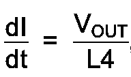
- c. Switch Q1 is conducting and passes inductor L1 current and diode D4 reverse recovery current.
- d. Volt-seconds are applied equally to reactor L3 and inductor L4, reaching VOUT x trr at the start of time 4.
- 4)
- a. Diode D4 stops conducting.
- b. V2 falls to zero at a rate determined by values of inductor L4 and capacitor C3 plus the internal capacitance of diode D4.
- c. The potential at point V3 is clamped to zero by diode D3.
- d. The reverse recovery current through diode D4 has stored energy in inductor L4 equal to


- 5)
- a. Energy in inductor L4 is transferred to capacitor C2 via diode D2. Capacitor C2 is charged from zero in a quarter cycle resonance of inductor L4 and capacitor C2.
Time interval
Peak voltage across capacitor C2 =
- b. During time 5, inductor L4 applies a voltage across the saturable reactor L3 through diode D1 equal to the voltage across capacitor C2. The flux density on inductor L4 returns to zero, and hence reactor L3 flux density returns to +BSAT.
- a. Energy in inductor L4 is transferred to capacitor C2 via diode D2. Capacitor C2 is charged from zero in a quarter cycle resonance of inductor L4 and capacitor C2.
- 6) V2 returns to zero whilst capacitor C2 remains charged.
- 7)
- a. Switch Q1 turns off, and the high frequency snubber composed of capacitor C1 and resistor R1 damps stray circuit LC resonances.
- b. Inductor L3 is taken further into saturation by the discharging of capacitor C3.
- c. Voltage on switch Q1 is clamped by diode D3 plus diode D5 to VOUT. Energy in inductor L2 is transferred via diode D3 to the output.
- 8) Inductor L1 current flows through capacitor C2 and diode D5 until capacitor C2 is discharged to the forward recovery voltage of diode D4. This is a relatively high rms ripple current, and capacitor C2 should be a good quality capacitor such as polypropylene.
- 9)
- a. Inductor L1 current flows through diode D4.
- b. Reverse recovery current of diode D5 appears as a forward current spike in diode D4.
- c. Capacitor C2 becomes fully discharged to zero, ready for the next cycle time 5.
- The choice of the value of capacitance C2 is a compromise between:
- a. lower capacitance whereby it will charge in a shorter time interval 5, allowing the boost convertor to be designed to operate at a higher switching frequency, and
- b. higher capacitance whereby there will be lower voltage stress on diode D4 but increasing time interval 5.
- If the minimum switch "on" time for the switch Q1 is less than the time interval 5, reactor L3 will still be at high impedance at when switch Q1 turns off. Current from inductor L1 will then flow through inductor L2 and diodes D3 and D5 to the output.
- The waveforms shown in Figure 7 are for circuit conditions with the following typical values of circuit components and operating conditions:
- VIN
- = 150V
- VOUT
- = 400V
- IIN
- = 6.5A
- L1
- = 800µH
- L4
- = 20µH
- C2
- = 33nF
- C3
- = 120pF
- Q1 "on" time
- = 5µs
- Q1 period
- = 8us
- D4 Irr
- = 2A
- D4 trr
- = 150ns
- time interval 5
- = 1.3µs
- time interval 8
- = 400ns.
- Circuit operation has been described for the particular circuit topology of a boost convertor. The invention, however, may be applied to any other switching power convertor employing a power switch and inductive current catch rectifier driving an inductive load, eg. a motor. The circuit 80 shown in Figure 8 is for a buck convertor according to the invention whilst the
circuit 90 shown in Figure 9 shows a full bridge invertor according to the invention used in un-interpretable power supplies. Again the same references are used for equivalent components in Figures 8 and 9 as are used in Figure 6. - In both circuits the inductive load L1 is driven by the switch Q1. Inductive current flows through the catch rectifier D4 and saturable reactor L3. When switch Q1 turns on, reactor L3 switches to it's high impedance state, and reverse current in rectifier D4 flows in to diode D1 and inductor L4. When diode D4 turns off after the time trr, energy stored in inductor L4 is used to drive the flux in reactor L3 back into saturation (+BSAT) whilst capacitor C2 is being charged up. The maximum reverse voltage across diode D4 is VIN plus the voltage across capacitor C2. When switch Q1 turns off, the reactor L3 is driven further into saturation by capacitor C3 discharging, and inductive load current flows through diode D5, capacitor C2 and reactor L3. When capacitor C2 is discharged by this current, diode D4 starts to conduct. Inductor L2 is a turn on snubber, diode D3 limits the voltage across the switch Q1 to VIN, and capacitor C1 and resistor R1 act as a high frequency snubber.
- Although the
circuit 90 shown in Figure 9 is a full bridge circuit, a half bridge circuit according to the invention is equally possible. Thus, for example, the right-hand side of thecircuit 90 shown in Figure 9 could be replaced with two series connected capacitors between VIN and ground, and thepoint 92 taken to the common point of the capacitors. - The invention may be applied to any switching power convertor employing a transformer for isolation. The
circuit 100 of Figure 10 shows a fly back convertor using the invention, thecircuit 110 of Figure 11 shows a forward convertor using the invention, and thecircuit 120 of Figure 12 shows a full bridge using the invention. - In these Figures the same references are used for equivalent parts used in Figure 6 and it is believed that circuit operation will be readily understood from the previous description.
- The improvement in rectifier performance is of particular advantage when the DC output voltage is high, e.g. 48V DC as used in communication equipment, requiring the use of high voltage rectifiers which have relatively long reverse recovery times. When the electronic switch closes, the rectifier reverse recovery current acts as a short circuit across the transformer secondary winding, resulting in a high surge current in the electronic switch. The improved rectifier circuit described above according to the invention reduces this surge current and reduces reverse voltage stress on the rectifier.
Claims (10)
- A rectifier circuit (60) comprising a rectifier (D4) intended to allow current to flow in a forward direction to an output (VOUT), a saturable inductor (L3) connected in series with the rectifier (D4) allowing the ready passage of current in the forward direction but blocking reverse recovery rectifier current, the saturable inductor (L3) being connected in parallel with a rectifier (D1) in series with inductor means (L4) through which reverse recovery rectifier current passes and for limiting that reverse recovery current, energy stored in those inductor means (L4) being used to re-set the saturable inductor (L3) to its saturation state for a subsequent flow of current in the forward direction, characterised in that capacitor means (C2) are connected across the inductor means (L4) for absorbing surplus energy from the inductor means (L4), and rectifier means (D5) are connected between the capacitor means (C2) and the output (VOUT) for guiding that surplus energy to the output (VOUT).
- A rectifier circuit as claimed in Claim 1 in which additional capacitor means (C3) arc provided across the rectifier (D4) to aid in re-setting of the saturable inductor (L3) to its saturation state, and/or to slow down the application of reverse potential across the rectifier (D4).
- A rectifier circuit as claimed in either preceding claim in which the power supplied to the rectifier is an alternating source of power.
- A rectifier circuit as claimed in Claim 3 in which the alternating source of power is the output from a transformer.
- A convertor circuit comprising a first inductor means (L1) to store energy which is repeatedly switched by an electronic switch (Q1), the switching controlling the energy stored in the first inductor means (L1) to be delivered to the output (VOUT), and at least one rectifier circuit (60) as claimed in any preceding claim through which the energy stored is delivered to the output (VOUT).
- A convertor circuit as claimed in Claim 5 in which the first inductor means (L1) are provided in series with the rectifier circuit (60) to charge an output capacitor (C4).
- A convertor circuit as claimed in Claim 5 or Claim 6 in which additional rectifier means (D3) are provided to clamp the voltage across the electronic switch (Q1) to the output voltage (VOUT) as a maximum.
- A convertor circuit as claimed in any of claims 5 to 7 in which current limiting means (L2) are provided in series with the switch (Q1) to limit the initial current when it turns on so that the voltage across it has time to fall before it passes a high current.
- A convertor circuit as claimed in Claim 8 in which the current limiting means (L2) are another saturable inductor in series with the switch (Q1).
- A convertor circuit as claimed in Claim 8 or Claim 9 as appendant to Claim 7 in which the energy in this additional inductor (L2) when the electronic switch (Q1) becomes non-conducting is dissipated through the additional rectifier means (D3) for use together with the output potential (VOUT).
Priority Applications (1)
| Application Number | Priority Date | Filing Date | Title |
|---|---|---|---|
| AT89306905T ATE84925T1 (en) | 1988-07-14 | 1989-07-07 | ENERGY SUPPLIES. |
Applications Claiming Priority (2)
| Application Number | Priority Date | Filing Date | Title |
|---|---|---|---|
| GB8816774 | 1988-07-14 | ||
| GB888816774A GB8816774D0 (en) | 1988-07-14 | 1988-07-14 | Power supplies |
Publications (2)
| Publication Number | Publication Date |
|---|---|
| EP0351144A1 EP0351144A1 (en) | 1990-01-17 |
| EP0351144B1 true EP0351144B1 (en) | 1993-01-20 |
Family
ID=10640448
Family Applications (1)
| Application Number | Title | Priority Date | Filing Date |
|---|---|---|---|
| EP89306905A Expired - Lifetime EP0351144B1 (en) | 1988-07-14 | 1989-07-07 | Power supplies |
Country Status (6)
| Country | Link |
|---|---|
| US (1) | US4977493A (en) |
| EP (1) | EP0351144B1 (en) |
| KR (1) | KR900002520A (en) |
| AT (1) | ATE84925T1 (en) |
| DE (1) | DE68904488D1 (en) |
| GB (1) | GB8816774D0 (en) |
Families Citing this family (54)
| Publication number | Priority date | Publication date | Assignee | Title |
|---|---|---|---|---|
| JPH03226115A (en) * | 1990-01-31 | 1991-10-07 | Mitsubishi Electric Corp | Pulse generating circuit |
| JP2680914B2 (en) * | 1990-05-10 | 1997-11-19 | 甲府日本電気株式会社 | Switching power supply circuit |
| US5055991A (en) * | 1990-10-12 | 1991-10-08 | Compaq Computer Corporation | Lossless snubber |
| US5148358A (en) * | 1991-04-03 | 1992-09-15 | Hughes Aircraft Company | Rectifier commutation current spike suppressor |
| JP3199423B2 (en) * | 1991-11-01 | 2001-08-20 | オリジン電気株式会社 | Resonant type forward converter |
| US5432431A (en) * | 1992-05-21 | 1995-07-11 | Vlt Corporation | Boost switching power conversion using saturable inductors |
| US5416687A (en) * | 1992-06-23 | 1995-05-16 | Delta Coventry Corporation | Power factor correction circuit for AC to DC power supply |
| US5307004A (en) * | 1992-07-06 | 1994-04-26 | Carsten Bruce W | Soft switching boost and buck regulators |
| SE500589C2 (en) * | 1992-10-22 | 1994-07-18 | Ericsson Telefon Ab L M | Low-loss boost converter through limited back current in the main diode |
| US6075331A (en) * | 1993-03-18 | 2000-06-13 | Imra America, Inc. | Systems and methods for managing energy of electric power supply systems |
| CN1035972C (en) * | 1993-04-06 | 1997-09-24 | 整流器技术太平洋Pty公司 | Snubber |
| AU687043B2 (en) * | 1993-04-06 | 1998-02-19 | Rectifier Technologies Pacific Pty Ltd | Snubber |
| US5414613A (en) * | 1993-08-20 | 1995-05-09 | Rem Technologies, Incorporated | Soft switching active snubber for semiconductor circuit operated in discontinuous conduction mode |
| US5481238A (en) * | 1994-04-19 | 1996-01-02 | Argus Technologies Ltd. | Compound inductors for use in switching regulators |
| US5543704A (en) * | 1994-06-08 | 1996-08-06 | Telefonaktiebolaget Lm Ericsson | Pulse width modulated DC-to-DC boost converter |
| IT1267729B1 (en) * | 1994-06-14 | 1997-02-07 | Zeltron Spa | SELF-POWERED FLAME DETECTOR |
| US6018471A (en) * | 1995-02-02 | 2000-01-25 | Integrated Environmental Technologies | Methods and apparatus for treating waste |
| JPH09103073A (en) * | 1995-10-05 | 1997-04-15 | Fujitsu Denso Ltd | Dc-dc converter |
| US5731966A (en) * | 1996-06-17 | 1998-03-24 | Lucent Technologies Inc. | Snubber circuit for rectifying diodes and method of operation thereof |
| US5673186A (en) * | 1996-07-01 | 1997-09-30 | Dsc Telecom L.P. | Apparatus for protecting multiple output rectifiers in a current-fed DC-to DC converter |
| KR100199506B1 (en) * | 1996-10-29 | 1999-06-15 | 윤문수 | A zero voltage/current switching circuit for reduced ripple current of the full-bridge dc/dc converter |
| KR100325760B1 (en) * | 1996-11-22 | 2002-06-28 | 윤종용 | Inverse peak voltage eliminating circuit |
| US5828559A (en) * | 1997-02-03 | 1998-10-27 | Chen; Keming | Soft switching active snubber |
| WO1998035432A1 (en) * | 1997-02-10 | 1998-08-13 | Tdk Corporation | Step-up switching power supply |
| US5864471A (en) * | 1997-03-28 | 1999-01-26 | Kammiller; Neil A. | Energy recovery circuit for use in a converter |
| AU729687B2 (en) * | 1997-07-10 | 2001-02-08 | Ian Victor Hegglun | Power supply |
| US5877947A (en) * | 1997-07-30 | 1999-03-02 | Lucent Technologies Inc. | Snubber circuit for a rectifier and method of operation thereof |
| FI113915B (en) * | 1997-09-25 | 2004-06-30 | Helvar Oy | Circuit for controlled recovery of the body diode |
| FI113919B (en) * | 1997-09-25 | 2004-06-30 | Helvar Oy | Power frequency converter from AC to AC |
| US5982638A (en) * | 1997-10-31 | 1999-11-09 | Astec International Limited | Single stage power converter with regenerative snubber and power factor correction |
| EP1237270A3 (en) * | 1998-02-05 | 2004-01-07 | Helvar Oy Ab | Controlled diode recovery circuit |
| DE19808637A1 (en) * | 1998-02-28 | 1999-09-09 | Bosch Gmbh Robert | DC / DC converter with a transformer and a choke |
| US5943224A (en) * | 1998-04-06 | 1999-08-24 | Lucent Technologies Inc. | Post regulator with energy recovery snubber and power supply employing the same |
| IL125328A0 (en) | 1998-07-13 | 1999-03-12 | Univ Ben Gurion | Modular apparatus for regulating the harmonics of current drawn from power lines |
| US6052294A (en) * | 1998-09-14 | 2000-04-18 | Lucent Technologies Inc. | Power supply snubber reset circuit |
| CA2377503A1 (en) | 1999-06-30 | 2001-01-11 | Peco Ii, Inc. | Diode recovery current suppression circuits |
| DE19937924A1 (en) * | 1999-08-11 | 2001-02-15 | Patent Treuhand Ges Fuer Elektrische Gluehlampen Mbh | Rectifier with center point feed |
| WO2001026207A2 (en) * | 1999-10-01 | 2001-04-12 | Online Power Supply, Inc. | Non-saturating magnetic element(s) power converters and surge protection |
| US6272025B1 (en) | 1999-10-01 | 2001-08-07 | Online Power Supply, Inc. | Individual for distributed non-saturated magnetic element(s) (referenced herein as NSME) power converters |
| US6952355B2 (en) | 2002-07-22 | 2005-10-04 | Ops Power Llc | Two-stage converter using low permeability magnetics |
| US6781352B2 (en) | 2002-12-16 | 2004-08-24 | International Rectifer Corporation | One cycle control continuous conduction mode PFC boost converter integrated circuit with integrated power switch and boost converter |
| CN101436828B (en) * | 2003-04-22 | 2012-05-09 | 三垦电气株式会社 | Power factor improving circuit |
| US20050248963A1 (en) * | 2004-05-07 | 2005-11-10 | Cheng Chung Y | Circuit for controlling the reverse recovery current in a blocking diode |
| US7633775B2 (en) * | 2004-12-10 | 2009-12-15 | General Electric Company | Power conversion system and method |
| US20070229047A1 (en) * | 2006-03-31 | 2007-10-04 | James Sigamani | Tapped inductor buck dc-dc converter |
| US7375984B2 (en) | 2006-06-16 | 2008-05-20 | Astec Custom Power (Hk) Ltd. | Zero voltage zero current switching converter |
| US20080071887A1 (en) * | 2006-09-19 | 2008-03-20 | Microsoft Corporation | Intelligent translation of electronic data interchange documents to extensible markup language representations |
| US7768243B2 (en) * | 2007-02-02 | 2010-08-03 | Stmicroelectronics S.A. | Aid for the switching of a switched-mode converter |
| JP4382859B1 (en) | 2008-06-23 | 2009-12-16 | サンケン電気株式会社 | DC-DC converter with snubber circuit |
| JP2010004704A (en) * | 2008-06-23 | 2010-01-07 | Sanken Electric Co Ltd | Dc-dc converter |
| US8111053B2 (en) | 2008-07-24 | 2012-02-07 | Sanken Electric Co., Ltd. | DC-DC converter |
| US8450892B2 (en) * | 2009-10-15 | 2013-05-28 | Hamilton Sundstrand Corporation | Synchronous generating machine with rectifier snubber circuit |
| JP5853366B2 (en) * | 2010-12-24 | 2016-02-09 | 富士通株式会社 | Power supply device, information processing device |
| DE102016106385A1 (en) * | 2016-04-07 | 2017-10-12 | Huf Hülsbeck & Fürst Gmbh & Co. Kg | Vehicle door handle with control circuit |
Family Cites Families (4)
| Publication number | Priority date | Publication date | Assignee | Title |
|---|---|---|---|---|
| US3955131A (en) * | 1975-09-08 | 1976-05-04 | General Electric Company | Circuit for controlling the reverse current in a controlled rectifier |
| US4230955A (en) * | 1978-04-06 | 1980-10-28 | Megapulse Incorporated | Method of and apparatus for eliminating priming and carrier sweep-out losses in SCR switching circuits and the like |
| DE3132512A1 (en) * | 1981-04-04 | 1983-03-10 | Andreas Prof. Dr.-Ing.habil. 7000 Stuttgart Boehringer | Simplified device, without any losses caused by the principle of operation, for ridding electrical or electronic one-way switches of a high power loss stress while they are switching on and off as well as ridding them of an increased cut-off voltage stress in conjunction with their switching off |
| US4591966A (en) * | 1983-05-19 | 1986-05-27 | Steve Smith | Rectifying network |
-
1988
- 1988-07-14 GB GB888816774A patent/GB8816774D0/en active Pending
-
1989
- 1989-07-07 EP EP89306905A patent/EP0351144B1/en not_active Expired - Lifetime
- 1989-07-07 AT AT89306905T patent/ATE84925T1/en not_active IP Right Cessation
- 1989-07-07 DE DE8989306905T patent/DE68904488D1/en not_active Expired - Lifetime
- 1989-07-13 US US07/379,380 patent/US4977493A/en not_active Expired - Lifetime
- 1989-07-14 KR KR1019890010037A patent/KR900002520A/en not_active Application Discontinuation
Also Published As
| Publication number | Publication date |
|---|---|
| US4977493A (en) | 1990-12-11 |
| EP0351144A1 (en) | 1990-01-17 |
| DE68904488D1 (en) | 1993-03-04 |
| KR900002520A (en) | 1990-02-28 |
| GB8816774D0 (en) | 1988-08-17 |
| ATE84925T1 (en) | 1993-02-15 |
Similar Documents
| Publication | Publication Date | Title |
|---|---|---|
| EP0351144B1 (en) | Power supplies | |
| US5959438A (en) | Soft-switched boost converter with isolated active snubber | |
| US5815386A (en) | Snubber for zero current switched networks | |
| USRE37889E1 (en) | Low loss synchronous rectifier for application to clamped-mode power converters | |
| US5448467A (en) | Electrical power converter circuit | |
| US6314002B1 (en) | Voltage clamping system and method for a DC/DC power converter | |
| US5636114A (en) | Lossless snubber circuit for use in power converters | |
| US5625541A (en) | Low loss synchronous rectifier for application to clamped-mode power converters | |
| EP1159781B1 (en) | General self-driven synchronous rectification scheme for synchronous rectifiers having a floating gate | |
| US4336587A (en) | High efficiency turn-off loss reduction network with active discharge of storage capacitor | |
| JP2773195B2 (en) | Switching power supply | |
| US5923152A (en) | Power factor correction circuit with soft switched boost converter | |
| US5287261A (en) | Power conversion using zero current soft switching | |
| US5132889A (en) | Resonant-transition DC-to-DC converter | |
| US4365171A (en) | Low loss snubber circuit | |
| US5418703A (en) | DC-DC converter with reset control for enhanced zero-volt switching | |
| EP0858150B1 (en) | Low cost high efficiency power converter | |
| US6249444B1 (en) | Offset resonant ZVS forward converter | |
| GB2388258A (en) | Switching power source device with overcurrent protection | |
| EP0746900A1 (en) | Improved continuous flyback power converter | |
| EP1188224A1 (en) | Single-ended forward converter circuit with quasi-optimal resetting for synchronous rectification | |
| US5063488A (en) | Switching power source means | |
| US5457379A (en) | High efficiency switch mode regulator | |
| US4669023A (en) | Apparatus for freeing electronic one-way switches from high power dissipation stresses | |
| KR200266522Y1 (en) | Energy regenerative snubber circuit for 2-switch forward converter |
Legal Events
| Date | Code | Title | Description |
|---|---|---|---|
| PUAI | Public reference made under article 153(3) epc to a published international application that has entered the european phase |
Free format text: ORIGINAL CODE: 0009012 |
|
| AK | Designated contracting states |
Kind code of ref document: A1 Designated state(s): AT CH DE ES FR GB IT LI NL SE |
|
| 17P | Request for examination filed |
Effective date: 19900622 |
|
| 17Q | First examination report despatched |
Effective date: 19911015 |
|
| GRAA | (expected) grant |
Free format text: ORIGINAL CODE: 0009210 |
|
| AK | Designated contracting states |
Kind code of ref document: B1 Designated state(s): AT CH DE ES FR GB IT LI NL SE |
|
| PG25 | Lapsed in a contracting state [announced via postgrant information from national office to epo] |
Ref country code: IT Free format text: LAPSE BECAUSE OF FAILURE TO SUBMIT A TRANSLATION OF THE DESCRIPTION OR TO PAY THE FEE WITHIN THE PRE;WARNING: LAPSES OF ITALIAN PATENTS WITH EFFECTIVE DATE BEFORE 2007 MAY HAVE OCCURRED AT ANY TIME BEFORE 2007. THE CORRECT EFFECTIVE DATE MAY BE DIFFERENT FROM THE ONE RECORDED.SCRIBED TIME-LIMIT Effective date: 19930120 Ref country code: NL Effective date: 19930120 Ref country code: ES Free format text: THE PATENT HAS BEEN ANNULLED BY A DECISION OF A NATIONAL AUTHORITY Effective date: 19930120 Ref country code: AT Effective date: 19930120 Ref country code: FR Effective date: 19930120 Ref country code: DE Effective date: 19930120 Ref country code: CH Effective date: 19930120 Ref country code: LI Effective date: 19930120 Ref country code: SE Effective date: 19930120 |
|
| REF | Corresponds to: |
Ref document number: 84925 Country of ref document: AT Date of ref document: 19930215 Kind code of ref document: T |
|
| REF | Corresponds to: |
Ref document number: 68904488 Country of ref document: DE Date of ref document: 19930304 |
|
| REG | Reference to a national code |
Ref country code: CH Ref legal event code: PL |
|
| EN | Fr: translation not filed | ||
| NLV1 | Nl: lapsed or annulled due to failure to fulfill the requirements of art. 29p and 29m of the patents act | ||
| PLBE | No opposition filed within time limit |
Free format text: ORIGINAL CODE: 0009261 |
|
| STAA | Information on the status of an ep patent application or granted ep patent |
Free format text: STATUS: NO OPPOSITION FILED WITHIN TIME LIMIT |
|
| 26N | No opposition filed | ||
| REG | Reference to a national code |
Ref country code: GB Ref legal event code: IF02 |
|
| PGFP | Annual fee paid to national office [announced via postgrant information from national office to epo] |
Ref country code: GB Payment date: 20020703 Year of fee payment: 14 |
|
| PG25 | Lapsed in a contracting state [announced via postgrant information from national office to epo] |
Ref country code: GB Free format text: LAPSE BECAUSE OF NON-PAYMENT OF DUE FEES Effective date: 20030707 |
|
| GBPC | Gb: european patent ceased through non-payment of renewal fee |
Effective date: 20030707 |