EP0349836B1 - A guarded electronic circuit from reversal of its supply battery polarity - Google Patents
A guarded electronic circuit from reversal of its supply battery polarity Download PDFInfo
- Publication number
- EP0349836B1 EP0349836B1 EP89111329A EP89111329A EP0349836B1 EP 0349836 B1 EP0349836 B1 EP 0349836B1 EP 89111329 A EP89111329 A EP 89111329A EP 89111329 A EP89111329 A EP 89111329A EP 0349836 B1 EP0349836 B1 EP 0349836B1
- Authority
- EP
- European Patent Office
- Prior art keywords
- transistor
- circuit
- battery
- load
- reversal
- Prior art date
- Legal status (The legal status is an assumption and is not a legal conclusion. Google has not performed a legal analysis and makes no representation as to the accuracy of the status listed.)
- Expired - Lifetime
Links
- 230000001939 inductive effect Effects 0.000 description 3
- 230000001965 increasing effect Effects 0.000 description 2
- XUIMIQQOPSSXEZ-UHFFFAOYSA-N Silicon Chemical compound [Si] XUIMIQQOPSSXEZ-UHFFFAOYSA-N 0.000 description 1
- 230000001154 acute effect Effects 0.000 description 1
- 238000010586 diagram Methods 0.000 description 1
- 238000011900 installation process Methods 0.000 description 1
- 230000010354 integration Effects 0.000 description 1
- 238000004519 manufacturing process Methods 0.000 description 1
- 229910052710 silicon Inorganic materials 0.000 description 1
- 239000010703 silicon Substances 0.000 description 1
Images
Classifications
-
- H—ELECTRICITY
- H02—GENERATION; CONVERSION OR DISTRIBUTION OF ELECTRIC POWER
- H02H—EMERGENCY PROTECTIVE CIRCUIT ARRANGEMENTS
- H02H11/00—Emergency protective circuit arrangements for preventing the switching-on in case an undesired electric working condition might result
- H02H11/002—Emergency protective circuit arrangements for preventing the switching-on in case an undesired electric working condition might result in case of inverted polarity or connection; with switching for obtaining correct connection
- H02H11/003—Emergency protective circuit arrangements for preventing the switching-on in case an undesired electric working condition might result in case of inverted polarity or connection; with switching for obtaining correct connection using a field effect transistor as protecting element in one of the supply lines
Definitions
- This invention relates to an electronic circuit which is protected against reversal of the polarity of a supply battery, of a type comprising a power transistor to be connected between one pole of the battery and ground, to drive an electric load to ground.
- the various electric loads such as lights, actuators, and the like, are usually driven between a positive supply pole and ground via electronic control circuits.
- a unidirectional component specifically a diode
- a unidirectional component be connected between the positive supply pole and the electronic control circuit to protect such an integrated circuit in the event that the battery polarity is reversed.
- the transistor conductance is due not only to the forward biasing of the inherent diode but also to the conductive state taken by the transistor channel.
- DE-A-3,535,788 provides, in more detailed teaching the same suggestion and considers the use of either a P-channel MOSFET for connection between the positive pole and the load, or of a N-channel MOSFET for connection between the negative pole of the voltage source and the load.
- US-A-4,658,203 discloses a control circuit for an inductive load, where a power MOSFET is used, coupled between ground and an inductive load terminal, the other load terminal being connected to a positive voltage source.
- a voltage clamp circuit is provided to render the power MOSFET conductive if a positive inductive voltage appears at the junction between the load and the switch. However no protection, in the sense of preventing a reverse current flow in the load, in case of voltage reversal is provided.
- This document may be considered exemplary of the several problems involved in the protection against voltage reversal, of a load controlled by a circuit including a power MOSFET.
- the technical problem that underlies this invention is to provide an electronic integrated circuit having such structural and performance characteristics as to overcome the cited drawbacks of the prior art.
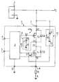
- circuit 1 embodying this invention, which is protected against reversal of the polarity of a supply battery 2.
- the circuit 1 is of the integrated kind and comprises a circuit portion 3, known per se, which is connected to an input pin 4 and to a pair of output pins 5 and 6, wherein the pin 6 is grounded.
- the circuit 1 also comprises a further input pin 7, connected to a positive supply pole Vc of the battery 2, and a further output pin 8 connected to one end of a resistor RL having the other end connected to ground.
- That resistor RL is representative of an electric load driven to ground by means of the circuit 1.
- the circuit 1 incorporates a first power transistor T1 of the enhancement, N-channel MOS type, which has its gate G1 and source S1 connected to the circuit portion 3.
- the source S1 is also connected to drive the load RL via the output pin 8.
- the transistor T1 includes an inherent diode D3, between the source S1 and the drain D1, which is biased forwardly toward the source S1.
- a second transistor T2 also of the N-channel MOS power type, is incorporated to the circuit 1, with its source S2 and drain D2 electrodes respectively connected to the positive pole Vc, through the input pin 7, and to the drain D1 of the first transistor T1.
- the gate G2 of the second transistor T2 is in turn connected to the circuit portion 3.
- the transistor T2 also has an inherent diode D4 between the source S2 and the drain D2, and is biased forwardly toward the source S2.
- the circuit 1 is provided with devices 9 and 10 for protection against possible positive or negative overvoltages from the battery 2.
- the device 10 comprises a pair of Zener diodes Z1 and Z2, connected serially to each other and in push-pull configuration between the positive pole Vc and the gate G1 of the first transistor T1.
- the device 9 comprises, in turn, a pair of Zener diodes Z3 and Z4 interconnected in push-pull configuration, between the gate G2 and the drain D2 of the second transistor T2.
- the second transistor is conducting at all times when the supply voltage Vc has the correct polarity, and will protect the integrated circuit 1 in all those cases where the polarity of the battery 2 is reversed.
- a current IL flows through the load RL which is supplied from the first transistor T1 via the second protection transistor T2.
- the second transistor On the polarity of the battery 2 being reversed, the second transistor will change to a break state and protect both the circuit 1 and the load RL.
- the voltage drop V across the second transistor may be made as small as desired, since it results from the product of the inherent resistance of the transistor T2 multiplied by the load current IL flowing therethrough. Since the value of this resistance is tied inversely to the silicon area occupied by that second transistor in the integrated circuit 1, this resistive value may be made quite small by increasing the surface area occupied by the transistor and consequently reducing the voltage drop thereacross and the amount of electric power used up.
- the circuit of this invention has a major advantage in that it can protect itself against any reversals in the polarity of the supply battery to which it is connected, while also protecting the electric load driven thereby.
- This circuit also has an outstandingly simple structure, may be readily implemented as an integrated circuit, and is characteristically endowed with very small power dissipation.
Landscapes
- Charge And Discharge Circuits For Batteries Or The Like (AREA)
- Emergency Protection Circuit Devices (AREA)
- Protection Of Static Devices (AREA)
- Electronic Switches (AREA)
Description
- This invention relates to an electronic circuit which is protected against reversal of the polarity of a supply battery, of a type comprising a power transistor to be connected between one pole of the battery and ground, to drive an electric load to ground.
- It is a well-recognized fact that car manufacturing procedures call for the addition of an electric system powering battery to each car during the final stages of the electric system installation process and assembly of the electric loads connected therein.
- The various electric loads, such as lights, actuators, and the like, are usually driven between a positive supply pole and ground via electronic control circuits.
- Since it is not unlikely for the cables which interconnect the supply to such circuits to be occasionally misled, there exists a demand for having the supply battery installed, even where polarity has been reversed, without endangering said integrated circuits.
- This need also arises from the likelihood that just the battery connections be reversed by mistake, and becomes specially acute where an integrated circuit includes power actuators including, inter alia, inherent transistors, for which no limiting resistive components can be provided in the supply line since these would lower the supply voltage in consequence of the voltage drop thereacross.
- To meet the above demand, it has been proposed that a unidirectional component, specifically a diode, be connected between the positive supply pole and the electronic control circuit to protect such an integrated circuit in the event that the battery polarity is reversed.
- While being advantageous cost-wise, this prior approach has a drawback in that the voltage drop Vd across the diode lowers the voltage available to the electric load to be driven, and that the overall efficiency of the system deteriorates due to the power requirements being increased by an amount equal to the product of the voltage Vd across the diode multiplied by the current IL flowing through the load.
- In US-A-4,423,456 it has been proposed to connect a protection MOS type transistor in series between the positive pole of a power supply and a device to be protected, the protection transistor being driven in break state when the polarity of the DC power supply is reversed and being conductive when the voltage is properly applied.
- The transistor conductance is due not only to the forward biasing of the inherent diode but also to the conductive state taken by the transistor channel.
- DE-A-3,535,788 provides, in more detailed teaching the same suggestion and considers the use of either a P-channel MOSFET for connection between the positive pole and the load, or of a N-channel MOSFET for connection between the negative pole of the voltage source and the load.
- In this way the voltage drop across the protection transistor can be lowered but the problems of possible integration of the protection device in a control circuit controlling the energization of the load and still having the load grounded are not considered, nor is a solution to such problems suggested.
- US-A-4,658,203 discloses a control circuit for an inductive load, where a power MOSFET is used, coupled between ground and an inductive load terminal, the other load terminal being connected to a positive voltage source.
- A voltage clamp circuit is provided to render the power MOSFET conductive if a positive inductive voltage appears at the junction between the load and the switch. However no protection, in the sense of preventing a reverse current flow in the load, in case of voltage reversal is provided.
- This document may be considered exemplary of the several problems involved in the protection against voltage reversal, of a load controlled by a circuit including a power MOSFET.
- In US-A-4,658,203 a voltage reversal of the power supply would cause current conduction through the inherent diode of the power MOSFET and the load, with possible damage of the same and in any event uncontrolled energization of the load.
- Further, under properly applied powering, when the power MOSFET is switched off the load is disconnected from ground and remains connected to the positive pole of the voltage source, a situation which is to be avoided in automotive electrical equipment for safety reasons.
- A combination of the teaching of the above documents would be possible but the result would not lead to the reconciliation of the several requirements of safety, efficiency and integrability of the protection device and the control circuit in a single component.
- The technical problem that underlies this invention is to provide an electronic integrated circuit having such structural and performance characteristics as to overcome the cited drawbacks of the prior art.
- This problem is solved by a circuit as indicated in the appended
claim 1. - The features and advantages of a circuit according to the invention will become apparent from the following detailed description of an embodiment thereof, given by way of illustration and not of limitation with reference to the accompanying drawing.
- Shown in the drawing is a diagram of the inventive circuit.
- With reference to the drawing view, generally and schematically indicated at 1 is a circuit, embodying this invention, which is protected against reversal of the polarity of a
supply battery 2. - The
circuit 1 is of the integrated kind and comprises acircuit portion 3, known per se, which is connected to aninput pin 4 and to a pair of output pins 5 and 6, wherein the pin 6 is grounded. - The
circuit 1 also comprises a further input pin 7, connected to a positive supply pole Vc of thebattery 2, and a further output pin 8 connected to one end of a resistor RL having the other end connected to ground. - That resistor RL is representative of an electric load driven to ground by means of the
circuit 1. - The
circuit 1 incorporates a first power transistor T1 of the enhancement, N-channel MOS type, which has its gate G1 and source S1 connected to thecircuit portion 3. The source S1 is also connected to drive the load RL via the output pin 8. - The transistor T1 includes an inherent diode D3, between the source S1 and the drain D1, which is biased forwardly toward the source S1.
- According to the invention, a second transistor T2, also of the N-channel MOS power type, is incorporated to the
circuit 1, with its source S2 and drain D2 electrodes respectively connected to the positive pole Vc, through the input pin 7, and to the drain D1 of the first transistor T1. The gate G2 of the second transistor T2 is in turn connected to thecircuit portion 3. - The transistor T2 also has an inherent diode D4 between the source S2 and the drain D2, and is biased forwardly toward the source S2.
- In addition, the
circuit 1 is provided withdevices 9 and 10 for protection against possible positive or negative overvoltages from thebattery 2. Thedevice 10 comprises a pair of Zener diodes Z1 and Z2, connected serially to each other and in push-pull configuration between the positive pole Vc and the gate G1 of the first transistor T1. - The device 9 comprises, in turn, a pair of Zener diodes Z3 and Z4 interconnected in push-pull configuration, between the gate G2 and the drain D2 of the second transistor T2.
- The second transistor is conducting at all times when the supply voltage Vc has the correct polarity, and will protect the integrated
circuit 1 in all those cases where the polarity of thebattery 2 is reversed. - In operation of the
circuit 1, a current IL flows through the load RL which is supplied from the first transistor T1 via the second protection transistor T2. - On the polarity of the
battery 2 being reversed, the second transistor will change to a break state and protect both thecircuit 1 and the load RL. - Advantageously, the voltage drop V across the second transistor may be made as small as desired, since it results from the product of the inherent resistance of the transistor T2 multiplied by the load current IL flowing therethrough. Since the value of this resistance is tied inversely to the silicon area occupied by that second transistor in the
integrated circuit 1, this resistive value may be made quite small by increasing the surface area occupied by the transistor and consequently reducing the voltage drop thereacross and the amount of electric power used up. - Thus, the circuit of this invention has a major advantage in that it can protect itself against any reversals in the polarity of the supply battery to which it is connected, while also protecting the electric load driven thereby.
- This circuit also has an outstandingly simple structure, may be readily implemented as an integrated circuit, and is characteristically endowed with very small power dissipation.
Claims (2)
- An integrated electronic circuit (1) which is protected against reversal of the polarity of a supply battery (2), of a type comprising a first MOS-type power transistor (T1) with inherent diode (D3) to be connected in series with a load (RL) between a pole (Vc) of said battery (2) and ground, to drive said electrical load, characterized in that said circuit (1) comprises a second protection N-channel MOS-type transistor (T2) with inherent diode (D4), said second transistor (T2) having its source (S2) connected to an input pin (7) of the circuit (1) for connection to said pole (Vc) of the battery (2) and its drain (D2) series connected to said first transistor (T1), said transistors (T1,T2) having their inherent diodes (D3,D4) biased in opposed directions and said second transistor (T2) being controlled by the circuit (1) to be in a break state upon polarity reversal of said battery (2).
- A circuit according to claim 1 where said first and second transistor (T1,T2) are both of the N-channel MOS type, with their respective drain electrodes (D1,D2) connected to each other.
Applications Claiming Priority (2)
| Application Number | Priority Date | Filing Date | Title |
|---|---|---|---|
| IT8821235A IT1226439B (en) | 1988-07-05 | 1988-07-05 | ELECTRONIC CIRCUIT PROTECTED FROM POLARITY REVERSAL OF THE POWER BATTERY. |
| IT2123588 | 1988-07-05 |
Publications (3)
| Publication Number | Publication Date |
|---|---|
| EP0349836A2 EP0349836A2 (en) | 1990-01-10 |
| EP0349836A3 EP0349836A3 (en) | 1991-03-27 |
| EP0349836B1 true EP0349836B1 (en) | 1994-08-03 |
Family
ID=11178816
Family Applications (1)
| Application Number | Title | Priority Date | Filing Date |
|---|---|---|---|
| EP89111329A Expired - Lifetime EP0349836B1 (en) | 1988-07-05 | 1989-06-22 | A guarded electronic circuit from reversal of its supply battery polarity |
Country Status (5)
| Country | Link |
|---|---|
| US (1) | US4958251A (en) |
| EP (1) | EP0349836B1 (en) |
| JP (1) | JP2770988B2 (en) |
| DE (1) | DE68917226T2 (en) |
| IT (1) | IT1226439B (en) |
Families Citing this family (33)
| Publication number | Priority date | Publication date | Assignee | Title |
|---|---|---|---|---|
| IT1226438B (en) * | 1988-07-05 | 1991-01-15 | Sgs Thomson Microelectronics | ELECTRONIC CIRCUIT WITH DEVICE FOR PROTECTION FROM VOLTAGE VARIATIONS OF THE POWER BATTERY. |
| IT1227104B (en) * | 1988-09-27 | 1991-03-15 | Sgs Thomson Microelectronics | SELF-PROTECTED INTEGRATED CIRCUIT FROM POLARITY INVERSIONS OF THE POWER BATTERY |
| US5179492A (en) * | 1990-03-30 | 1993-01-12 | Pioneer Electronic Corporation | Protection circuit for detachable operating unit used in audio device |
| DE59105964D1 (en) * | 1990-07-24 | 1995-08-17 | Ifm Electronic Gmbh | Electronic switching device with presence indicator. |
| JPH04156226A (en) * | 1990-10-17 | 1992-05-28 | Nippon Denki Musen Denshi Kk | Inverse connection preventing switching circuit |
| EP0487759B1 (en) * | 1990-11-26 | 1995-04-26 | Siemens Aktiengesellschaft | Reverse battery protection |
| DE4137452A1 (en) * | 1991-11-14 | 1993-05-19 | Bosch Gmbh Robert | POLE PROTECTION ARRANGEMENT FOR POWER AMPLIFIER FIELD EFFECT TRANSISTORS |
| US5410441A (en) * | 1993-02-01 | 1995-04-25 | Motorola, Inc. | Circuit for protecting DC powered devices from improper supply voltages |
| US5434739A (en) * | 1993-06-14 | 1995-07-18 | Motorola, Inc. | Reverse battery protection circuit |
| DE4432957C1 (en) * | 1994-09-16 | 1996-04-04 | Bosch Gmbh Robert | Switching means |
| JP3485655B2 (en) * | 1994-12-14 | 2004-01-13 | 株式会社ルネサステクノロジ | Composite MOSFET |
| DE19509024C1 (en) * | 1995-03-13 | 1996-10-31 | Sgs Thomson Microelectronics | Integrated semiconductor circuit (controllable semiconductor switch) with protection against negative potential |
| US5781390A (en) * | 1996-12-21 | 1998-07-14 | Sgs-Thomson Microelectronics, Inc. | Integrated supply protection |
| DE19803040A1 (en) * | 1997-01-31 | 1998-08-06 | Int Rectifier Corp | Power switching |
| US5847911A (en) * | 1997-11-20 | 1998-12-08 | Trw Inc. | Self-protecting switch apparatus for controlling a heat element of a vehicle seat and a method for providing the apparatus |
| DE19817790A1 (en) * | 1998-04-21 | 1999-12-09 | Siemens Ag | Reverse polarity protection circuit |
| DE19938403C2 (en) * | 1999-08-13 | 2002-03-14 | Micronas Gmbh | circuit |
| JP3926975B2 (en) * | 1999-09-22 | 2007-06-06 | 株式会社東芝 | Stacked MOS transistor protection circuit |
| US6611410B1 (en) | 1999-12-17 | 2003-08-26 | Siemens Vdo Automotive Inc. | Positive supply lead reverse polarity protection circuit |
| US6342805B1 (en) | 2000-06-15 | 2002-01-29 | Rockwell Automation Technologies, Inc. | System and method for selectively connecting one of at least two outputs of an associated circuit to an output node |
| DE10048184A1 (en) * | 2000-09-28 | 2002-04-11 | Delphi Tech Inc | Reverse voltage protection circuit |
| EP1357658B8 (en) * | 2002-04-22 | 2009-12-16 | Semiconductor Components Industries, LLC | Protection circuit against voltage transients and polarity reversal |
| DE50311044D1 (en) * | 2003-02-27 | 2009-02-26 | Delphi Tech Inc | Electronic protection circuit |
| KR100513380B1 (en) * | 2003-12-05 | 2005-09-06 | 주식회사 팬택앤큐리텔 | Over voltage protection apparatus in a portable machinery |
| DE102005040072B9 (en) * | 2005-08-24 | 2012-02-09 | Infineon Technologies Ag | Device for polarity-safe supply of an electronic component with an intermediate voltage from a supply voltage |
| JP4805869B2 (en) * | 2007-03-30 | 2011-11-02 | 三菱農機株式会社 | Working vehicle |
| JP2008244487A (en) * | 2008-04-21 | 2008-10-09 | Renesas Technology Corp | Composite MOSFET |
| JP5368283B2 (en) * | 2009-12-03 | 2013-12-18 | プライムアースEvエナジー株式会社 | Voltage detection circuit |
| US8274227B2 (en) | 2010-05-06 | 2012-09-25 | Nextek Power Systems, Inc. | High-efficiency DC ballast arrangement with automatic polarity protection and emergency back-up for lighting fixture in a suspended DC-powered ceiling system |
| JP5772776B2 (en) * | 2012-09-28 | 2015-09-02 | 株式会社オートネットワーク技術研究所 | Power supply control device |
| US9472948B2 (en) * | 2013-09-30 | 2016-10-18 | Infineon Technologies Ag | On chip reverse polarity protection compliant with ISO and ESD requirements |
| JP2015165745A (en) * | 2014-03-03 | 2015-09-17 | オムロンオートモーティブエレクトロニクス株式会社 | power supply circuit |
| CN104917144A (en) * | 2015-06-04 | 2015-09-16 | 科力远混合动力技术有限公司 | Relay control circuit in high-voltage system for hybrid electric vehicle |
Citations (1)
| Publication number | Priority date | Publication date | Assignee | Title |
|---|---|---|---|---|
| DE3535788A1 (en) * | 1985-09-03 | 1986-02-20 | Siemens AG, 1000 Berlin und 8000 München | Incorrect polarity protection for circuit arrangements |
Family Cites Families (7)
| Publication number | Priority date | Publication date | Assignee | Title |
|---|---|---|---|---|
| US3829709A (en) * | 1973-08-31 | 1974-08-13 | Micro Components Corp | Supply reversal protecton circuit |
| US3940785A (en) * | 1974-05-06 | 1976-02-24 | Sprague Electric Company | Semiconductor I.C. with protection against reversed power supply |
| JPS5829697B2 (en) * | 1978-12-11 | 1983-06-24 | 株式会社ゼニライトブイ | electronic circuit protection device |
| US4423456A (en) * | 1981-11-13 | 1983-12-27 | Medtronic, Inc. | Battery reversal protection |
| US4473757A (en) * | 1981-12-08 | 1984-09-25 | Intersil, Inc. | Circuit means for converting a bipolar input to a unipolar output |
| US4658203A (en) * | 1984-12-04 | 1987-04-14 | Airborne Electronics, Inc. | Voltage clamp circuit for switched inductive loads |
| US4839769A (en) * | 1988-05-09 | 1989-06-13 | Motorola, Inc. | Driver protection circuit |
-
1988
- 1988-07-05 IT IT8821235A patent/IT1226439B/en active
-
1989
- 1989-06-22 EP EP89111329A patent/EP0349836B1/en not_active Expired - Lifetime
- 1989-06-22 DE DE68917226T patent/DE68917226T2/en not_active Expired - Fee Related
- 1989-06-23 US US07/370,445 patent/US4958251A/en not_active Expired - Lifetime
- 1989-07-05 JP JP1172111A patent/JP2770988B2/en not_active Expired - Fee Related
Patent Citations (1)
| Publication number | Priority date | Publication date | Assignee | Title |
|---|---|---|---|---|
| DE3535788A1 (en) * | 1985-09-03 | 1986-02-20 | Siemens AG, 1000 Berlin und 8000 München | Incorrect polarity protection for circuit arrangements |
Also Published As
| Publication number | Publication date |
|---|---|
| DE68917226T2 (en) | 1994-11-17 |
| JP2770988B2 (en) | 1998-07-02 |
| IT8821235A0 (en) | 1988-07-05 |
| EP0349836A3 (en) | 1991-03-27 |
| DE68917226D1 (en) | 1994-09-08 |
| IT1226439B (en) | 1991-01-15 |
| JPH0265625A (en) | 1990-03-06 |
| US4958251A (en) | 1990-09-18 |
| EP0349836A2 (en) | 1990-01-10 |
Similar Documents
| Publication | Publication Date | Title |
|---|---|---|
| EP0349836B1 (en) | A guarded electronic circuit from reversal of its supply battery polarity | |
| EP0854555B1 (en) | Integrated supply protection | |
| US7038522B2 (en) | System and method for redundant power supply connection | |
| EP0349837B1 (en) | An electronic circuit with a protection device against fluctuations in the supply battery voltage | |
| US6304422B1 (en) | Polarity reversal protection circuit | |
| US4808839A (en) | Power field effect transistor driver circuit for protection from overvoltages | |
| EP0115002B1 (en) | Voltage transient protection circuit | |
| KR19980064368A (en) | High Side MOSFET Gate Protection Sorter Circuit | |
| JP2001224135A (en) | Load drive | |
| US6614262B2 (en) | Failsafe interface circuit with extended drain devices | |
| EP3723289B1 (en) | Load drive circuit | |
| CN1089403A (en) | Switching device | |
| US5923210A (en) | High side driver circuit with diagnostic output | |
| EP0341460B1 (en) | Driver protection circuit | |
| CN112075001A (en) | Motor grounding protection | |
| US6414515B1 (en) | Failsafe interface circuit with extended drain devices | |
| US10879691B2 (en) | Unlockable switch inhibitor | |
| US5287024A (en) | FET bidirectional switching arrangements and methods for preventing pn junctions of FETs from being forward-biased | |
| JPH0644186Y2 (en) | MOSFET protection circuit | |
| WO2005117509A2 (en) | High current charge pump for intelligent power switch driver | |
| KR200152288Y1 (en) | Signal line switching control circuit | |
| JP3629175B2 (en) | Power supply control device | |
| JPH0775327A (en) | Load driver circuit |
Legal Events
| Date | Code | Title | Description |
|---|---|---|---|
| PUAI | Public reference made under article 153(3) epc to a published international application that has entered the european phase |
Free format text: ORIGINAL CODE: 0009012 |
|
| AK | Designated contracting states |
Kind code of ref document: A2 Designated state(s): DE FR GB NL SE |
|
| PUAL | Search report despatched |
Free format text: ORIGINAL CODE: 0009013 |
|
| AK | Designated contracting states |
Kind code of ref document: A3 Designated state(s): DE FR GB NL SE |
|
| 17P | Request for examination filed |
Effective date: 19910523 |
|
| 17Q | First examination report despatched |
Effective date: 19921229 |
|
| GRAA | (expected) grant |
Free format text: ORIGINAL CODE: 0009210 |
|
| AK | Designated contracting states |
Kind code of ref document: B1 Designated state(s): DE FR GB NL SE |
|
| REF | Corresponds to: |
Ref document number: 68917226 Country of ref document: DE Date of ref document: 19940908 |
|
| ET | Fr: translation filed | ||
| EAL | Se: european patent in force in sweden |
Ref document number: 89111329.2 |
|
| PLBE | No opposition filed within time limit |
Free format text: ORIGINAL CODE: 0009261 |
|
| STAA | Information on the status of an ep patent application or granted ep patent |
Free format text: STATUS: NO OPPOSITION FILED WITHIN TIME LIMIT |
|
| 26N | No opposition filed | ||
| REG | Reference to a national code |
Ref country code: FR Ref legal event code: D6 |
|
| REG | Reference to a national code |
Ref country code: GB Ref legal event code: IF02 |
|
| PGFP | Annual fee paid to national office [announced via postgrant information from national office to epo] |
Ref country code: FR Payment date: 20020610 Year of fee payment: 14 |
|
| PGFP | Annual fee paid to national office [announced via postgrant information from national office to epo] |
Ref country code: SE Payment date: 20020611 Year of fee payment: 14 |
|
| PGFP | Annual fee paid to national office [announced via postgrant information from national office to epo] |
Ref country code: GB Payment date: 20020619 Year of fee payment: 14 |
|
| PGFP | Annual fee paid to national office [announced via postgrant information from national office to epo] |
Ref country code: DE Payment date: 20020626 Year of fee payment: 14 |
|
| PG25 | Lapsed in a contracting state [announced via postgrant information from national office to epo] |
Ref country code: GB Free format text: LAPSE BECAUSE OF NON-PAYMENT OF DUE FEES Effective date: 20030622 |
|
| PG25 | Lapsed in a contracting state [announced via postgrant information from national office to epo] |
Ref country code: SE Free format text: LAPSE BECAUSE OF NON-PAYMENT OF DUE FEES Effective date: 20030623 |
|
| PGFP | Annual fee paid to national office [announced via postgrant information from national office to epo] |
Ref country code: NL Payment date: 20030630 Year of fee payment: 15 |
|
| PG25 | Lapsed in a contracting state [announced via postgrant information from national office to epo] |
Ref country code: DE Free format text: LAPSE BECAUSE OF NON-PAYMENT OF DUE FEES Effective date: 20040101 |
|
| EUG | Se: european patent has lapsed | ||
| GBPC | Gb: european patent ceased through non-payment of renewal fee |
Effective date: 20030622 |
|
| PG25 | Lapsed in a contracting state [announced via postgrant information from national office to epo] |
Ref country code: FR Free format text: LAPSE BECAUSE OF NON-PAYMENT OF DUE FEES Effective date: 20040227 |
|
| REG | Reference to a national code |
Ref country code: FR Ref legal event code: ST |
|
| PG25 | Lapsed in a contracting state [announced via postgrant information from national office to epo] |
Ref country code: NL Free format text: LAPSE BECAUSE OF NON-PAYMENT OF DUE FEES Effective date: 20050101 |
|
| NLV4 | Nl: lapsed or anulled due to non-payment of the annual fee |
Effective date: 20050101 |