EP0349318A2 - Verfahren zum Herstellen integrierter Schaltungspackungen - Google Patents
Verfahren zum Herstellen integrierter Schaltungspackungen Download PDFInfo
- Publication number
- EP0349318A2 EP0349318A2 EP89306610A EP89306610A EP0349318A2 EP 0349318 A2 EP0349318 A2 EP 0349318A2 EP 89306610 A EP89306610 A EP 89306610A EP 89306610 A EP89306610 A EP 89306610A EP 0349318 A2 EP0349318 A2 EP 0349318A2
- Authority
- EP
- European Patent Office
- Prior art keywords
- integrated circuit
- tape
- coating
- deposition
- circuit packages
- Prior art date
- Legal status (The legal status is an assumption and is not a legal conclusion. Google has not performed a legal analysis and makes no representation as to the accuracy of the status listed.)
- Withdrawn
Links
Images
Classifications
-
- H10W74/43—
-
- H10W70/453—
-
- H10W74/01—
-
- H10W74/131—
-
- H10W72/07251—
-
- H10W72/20—
Definitions
- This invention relates to methods of making integrated circuit packages.
- the invention relates to methods of making integrated circuit packages using tape automated bonding (TAB).
- TAB tape automated bonding
- TAB is a process in which a tape of plastics material, e.g. a polyimide, is provided with a series of apertures, normally rectangular, at spaced positions along the centre of the tape.
- a strip of metal, e.g. copper, foil is then bonded to one side of the tape and the foil etched to form around each aperture a lead pattern carried by the tape.
- the leads extend inwardly beyond the edge of the aperture and at their inner ends provide inner lead bonds which are positioned in corresponding manner to the connection pads of an integrated circuit chip.
- the leads extend outwardly from the inner lead bonds to provide adjacent the edge of the aperture outer lead bonds positioned in corresponding manner to connection pads on a substrate, e.g. a printed circuit board, on which it is desired to mount the chip.
- the leads normally extend outwardly beyond the outer lead bond area and terminate in test pads.
- the prepared tape and a supply of chips are fed to an inner lead bonding machine wherein the inner lead bonds of each lead pattern are gang bonded to the connection pads of a respective chip.
- the tape with chips so attached is then fed to an outer lead bonding machine wherein each chip with its lead pattern attached is excised from the tape and the outer lead bonds of each lead pattern bonded to a respective set of connection pads on a substrate.
- the inner lead bonds or the chip connection pads are normally provided with so called bumps e.g. of gold.
- the TAB process results in the production of chips possessing high packaging density with an increased chip yield due to ease of test which adds value to the chips.
- the chips moreover have high bond strength and bond reliability and are producible at reduced cost due to elimination of secondary packaging i.e. packaging intended to protect the integrated circuit during the manufacturing process.
- a method of making integrated circuit packages using tape automated bonding wherein after bonding of each integrated circuit to a lead pattern on a tape a coating of moisture impervious material is formed on all exposed surfaces of the integrated circuit and its lead pattern by deposition from an ambient atmosphere.
- the material suitably comprises a nitride material.
- Deposition of the coating is suitably effected by magnetron sputtering or by microwave plasma assisted chemical vapour deposition.
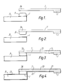
- a tape carrying a lead pattern for use in a TAB process for making integrated circuit packages is first prepared in conventional manner.
- connection pads 1 of the integrated circuit chips 3 may be provided with gold bumps 5 or alternatively the inner ends 7A, i.e. inner lead bonds of the leads 7 of the lead pattern, may be provided with gold pads 9, as shown in Figure 2.
- the tape 11 together with a supply of chips 3 is fed to an inner lead bonding machine (not shown) of conventional form and the inner lead bonds 7A bonded to the connection pads 1 on the chips 3, as shown in Figure 3.
- the outer lead bonds 7B of the leads 7 and the test pads (not shown) of the lead pattern, if present, are then provided with a protective coating 13, e.g. of wax, as shown in Figure 3.
- a protective coating 13 e.g. of wax
- the tape 11 with the chips 3 attached is then passed through a chamber (not shown) wherein the exposed surfaces of the chips 3 and leads 7 are provided with a coating of a nitride material 15 by deposition from an ambient atmosphere.
- the nitride material is any electrical insulating nitride material impervious to moisture such as a nitride of aluminium, boron silicon, germanium, gallium or indium.
- the tape 11 After removal of the protective coating 13, e.g. with a solvent, the tape 11 is fed to an outer lead bonding machine (not shown) wherein each chip 3 is excised from the tape 11 and bonded to a substrate 5 (now shown) in conventional manner.
- the nitride coating 15 is suitably deposited using a DC magnetron sputtering technique.
- the coating 15 may be deposited using a microwave plasma assisted chemical vapour deposition process. The latter comprises microwave heating of a mixture of nitrogen and the necessary precursor chemical vapours required to form a plasma from which the nitride coating is deposited.
- magnetron sputtering is cheaper than plasma deposition but affords less control over the composition of the nitride coating.
- the nitride coating forms an encapsulating coating impervious to water and salt ions present in water and other solvents liable to cause contamination and so reduce reliability of the chip.
- the gaseous nature of the deposition process is such that a uniform layer of material is provided of a few micrometers in thickness which contributes to the strength of the bond between the coating and the chip and its leads. Furthermore the nature of the deposition process is such as to have no material effect on the thermal or mechanical properties of the chip.
- a method according to the invention allows the use of a TAB process to mount integrated circuit chips directly on a substrate without the need for secondary packaging betwen the integrated circuit and substrate when environmental protection for the integrated circuit is required.
Landscapes
- Lead Frames For Integrated Circuits (AREA)
- Wire Bonding (AREA)
Applications Claiming Priority (2)
| Application Number | Priority Date | Filing Date | Title |
|---|---|---|---|
| GB8815704 | 1988-07-01 | ||
| GB888815704A GB8815704D0 (en) | 1988-07-01 | 1988-07-01 | Tape automated bonded microchips |
Publications (2)
| Publication Number | Publication Date |
|---|---|
| EP0349318A2 true EP0349318A2 (de) | 1990-01-03 |
| EP0349318A3 EP0349318A3 (de) | 1990-08-16 |
Family
ID=10639716
Family Applications (1)
| Application Number | Title | Priority Date | Filing Date |
|---|---|---|---|
| EP89306610A Withdrawn EP0349318A3 (de) | 1988-07-01 | 1989-06-29 | Verfahren zum Herstellen integrierter Schaltungspackungen |
Country Status (2)
| Country | Link |
|---|---|
| EP (1) | EP0349318A3 (de) |
| GB (1) | GB8815704D0 (de) |
Cited By (2)
| Publication number | Priority date | Publication date | Assignee | Title |
|---|---|---|---|---|
| EP0532898A3 (en) * | 1991-09-17 | 1993-07-21 | International Business Machines Corporation | Flex tape protective coating |
| US8674462B2 (en) | 2007-07-25 | 2014-03-18 | Infineon Technologies Ag | Sensor package |
Family Cites Families (4)
| Publication number | Priority date | Publication date | Assignee | Title |
|---|---|---|---|---|
| JPS5627941A (en) * | 1979-08-17 | 1981-03-18 | Hitachi Ltd | Manufacture of semiconductor device |
| JPS57210646A (en) * | 1981-06-19 | 1982-12-24 | Seiko Epson Corp | Resin-sealed semiconductor device |
| JPS59231840A (ja) * | 1983-06-14 | 1984-12-26 | Semiconductor Energy Lab Co Ltd | 半導体装置作成方法 |
| JPS62232947A (ja) * | 1986-04-02 | 1987-10-13 | Hitachi Ltd | 樹脂封止型半導体装置 |
-
1988
- 1988-07-01 GB GB888815704A patent/GB8815704D0/en active Pending
-
1989
- 1989-06-29 EP EP89306610A patent/EP0349318A3/de not_active Withdrawn
Cited By (3)
| Publication number | Priority date | Publication date | Assignee | Title |
|---|---|---|---|---|
| EP0532898A3 (en) * | 1991-09-17 | 1993-07-21 | International Business Machines Corporation | Flex tape protective coating |
| US8674462B2 (en) | 2007-07-25 | 2014-03-18 | Infineon Technologies Ag | Sensor package |
| US9379033B2 (en) | 2007-07-25 | 2016-06-28 | Infineon Technologies Ag | Sensor package |
Also Published As
| Publication number | Publication date |
|---|---|
| EP0349318A3 (de) | 1990-08-16 |
| GB8815704D0 (en) | 1988-08-10 |
Similar Documents
| Publication | Publication Date | Title |
|---|---|---|
| US3258898A (en) | Electronic subassembly | |
| US4727633A (en) | Method of securing metallic members together | |
| US4530152A (en) | Method for encapsulating semiconductor components using temporary substrates | |
| US7863757B2 (en) | Methods and systems for packaging integrated circuits | |
| US4012832A (en) | Method for non-destructive removal of semiconductor devices | |
| US6228686B1 (en) | Method of fabricating a microelectronic assembly using sheets with gaps to define lead regions | |
| US3614832A (en) | Decal connectors and methods of forming decal connections to solid state devices | |
| EP0502887B1 (de) | Packung mit metallstiftmuster und dielektrischer polymerdichtung | |
| US8021920B2 (en) | Method for producing a metal-ceramic substrate for electric circuits on modules | |
| EP0058068B1 (de) | Träger für integrierte Schaltungschips | |
| US20050017374A1 (en) | Semiconductor component of semiconductor chip size with flip-chip-like external contacts, and method of producing the same | |
| US20080315376A1 (en) | Conformal EMI shielding with enhanced reliability | |
| US6287894B1 (en) | Acoustic device packaged at wafer level | |
| US6323062B1 (en) | Wafer coating method for flip chips | |
| US10818805B2 (en) | Semiconductor sensor device and method for fabricating the same | |
| US20070134471A1 (en) | Methods and apparatuses for releasably attaching microfeature workpieces to support members | |
| US7368324B2 (en) | Method of manufacturing self-supporting contacting structures | |
| US20040018667A1 (en) | Method and apparatus for producing a silicon wafer chip package | |
| US6891252B2 (en) | Electronic component with a semiconductor chip and method of producing an electronic component | |
| EP0349318A2 (de) | Verfahren zum Herstellen integrierter Schaltungspackungen | |
| US20100133577A1 (en) | Method for producing electronic component and electronic component | |
| US7071571B2 (en) | Semiconductor component having a plastic housing and methods for its production | |
| US11437309B2 (en) | Method of manufacturing semiconductor devices and corresponding semiconductor device | |
| US5512780A (en) | Inorganic chip-to-package interconnection circuit | |
| GB2276977A (en) | Reducing thermal stress in I.C. chip mountings |
Legal Events
| Date | Code | Title | Description |
|---|---|---|---|
| PUAI | Public reference made under article 153(3) epc to a published international application that has entered the european phase |
Free format text: ORIGINAL CODE: 0009012 |
|
| AK | Designated contracting states |
Kind code of ref document: A2 Designated state(s): DE FR GB IT |
|
| PUAL | Search report despatched |
Free format text: ORIGINAL CODE: 0009013 |
|
| AK | Designated contracting states |
Kind code of ref document: A3 Designated state(s): DE FR GB IT |
|
| STAA | Information on the status of an ep patent application or granted ep patent |
Free format text: STATUS: THE APPLICATION IS DEEMED TO BE WITHDRAWN |
|
| 18D | Application deemed to be withdrawn |
Effective date: 19910219 |