EP0348893B1 - High speed non-volatile memory device - Google Patents
High speed non-volatile memory device Download PDFInfo
- Publication number
- EP0348893B1 EP0348893B1 EP89111676A EP89111676A EP0348893B1 EP 0348893 B1 EP0348893 B1 EP 0348893B1 EP 89111676 A EP89111676 A EP 89111676A EP 89111676 A EP89111676 A EP 89111676A EP 0348893 B1 EP0348893 B1 EP 0348893B1
- Authority
- EP
- European Patent Office
- Prior art keywords
- column
- lines
- circuit
- field effect
- channel type
- Prior art date
- Legal status (The legal status is an assumption and is not a legal conclusion. Google has not performed a legal analysis and makes no representation as to the accuracy of the status listed.)
- Expired - Lifetime
Links
- 238000007599 discharging Methods 0.000 claims description 24
- 230000008878 coupling Effects 0.000 claims description 7
- 238000010168 coupling process Methods 0.000 claims description 7
- 238000005859 coupling reaction Methods 0.000 claims description 7
- 239000004065 semiconductor Substances 0.000 claims description 6
- 239000000758 substrate Substances 0.000 claims description 5
- 230000001902 propagating effect Effects 0.000 claims description 4
- 230000005669 field effect Effects 0.000 description 82
- 238000010586 diagram Methods 0.000 description 9
- 230000000295 complement effect Effects 0.000 description 8
- 238000003491 array Methods 0.000 description 3
- 230000006399 behavior Effects 0.000 description 3
- 230000015572 biosynthetic process Effects 0.000 description 1
- 230000003247 decreasing effect Effects 0.000 description 1
- 238000012986 modification Methods 0.000 description 1
- 230000004048 modification Effects 0.000 description 1
Images


Classifications
-
- G—PHYSICS
- G11—INFORMATION STORAGE
- G11C—STATIC STORES
- G11C17/00—Read-only memories programmable only once; Semi-permanent stores, e.g. manually-replaceable information cards
- G11C17/08—Read-only memories programmable only once; Semi-permanent stores, e.g. manually-replaceable information cards using semiconductor devices, e.g. bipolar elements
- G11C17/10—Read-only memories programmable only once; Semi-permanent stores, e.g. manually-replaceable information cards using semiconductor devices, e.g. bipolar elements in which contents are determined during manufacturing by a predetermined arrangement of coupling elements, e.g. mask-programmable ROM
- G11C17/12—Read-only memories programmable only once; Semi-permanent stores, e.g. manually-replaceable information cards using semiconductor devices, e.g. bipolar elements in which contents are determined during manufacturing by a predetermined arrangement of coupling elements, e.g. mask-programmable ROM using field-effect devices
-
- G—PHYSICS
- G11—INFORMATION STORAGE
- G11C—STATIC STORES
- G11C16/00—Erasable programmable read-only memories
- G11C16/02—Erasable programmable read-only memories electrically programmable
- G11C16/06—Auxiliary circuits, e.g. for writing into memory
- G11C16/24—Bit-line control circuits
Definitions
- This invention relates to a non-volatile memory device and, more particularly, to a discharging circuit for discharging the column lines except for that coupled to the access memory cell.
- FIG. 1 of the drawings A typical example of the read only memory device is illustrated in Fig. 1 of the drawings and largely comprises a memory cell array 1 having a plurality of memory cells M00 to M33, a row address decoder circuit 2, a column selector circuit 3, a column decoder circuit 4, and a sense amplifier circuit 5.
- the memory cells M00 to M33 are arranged in rows and columns, and the memory cells M00 to M33 arranged in the rows are respectively coupled to word lines WL0 to WL3.
- Column lines DL1, DL2 and DL3 are provided in association with the columns of the memory cells, respectively, and output lines of the column selector circuit 4 are labeled with YD0, YD1, YD2 and YD3, respectively.
- the memory cells in each row line are gated by each of the word lines, and the row address decoder circuit 2 selectively shifts the word lines between an active high voltage level and an inactive low voltage level.
- the column selector circuit 3 has a plurality of n-channel type field effect transistors 6, 7, 8 and 9 which are associated with the columns of the memory cells, respectively.
- the column selector circuit 4 has a plurality of series combination circuits each consisting of a NAND gate and an inverter circuit, and one of the NAND gates is responsive to a multiple-bit column address signal and the complementary signal thereof to send an active low voltage level to one of the inverter circuits.
- the inverter circuit supplied with the active low voltage level allows one of the n-channel type field effect transistors 6 to 9 to turn on, and the n-channel type field effect transistor thus turned on provides a conduction path to the sense amplifier circuit 5.
- the memory cells M00 to M33 are formed by n-channel type field effect transistors, respectively, and are grouped by threshold voltage level depending upon data bits stored therein. Namely, the memory cells M00, M11, M12, M23 and M33 respectively memorize data bits of logic "0" level, and, for this reason, are formed by n-channel type field effect transistors each having a relatively low threshold voltage level of, for example, 1 volt. On the other hand, data bits of logic "1" level are stored in the memory cells M01, M02, M03, M10, M13, M20, M21, M22, M30, M31 and M32, respectively, so that the n-channel type field effect transistors thereof have a relatively high threshold voltage level of, for example, 10 volts.
- the row and column address signals firstly cause the row address decoder circuit 2 and the column selector circuit 4 to produce the active high voltage levels applied to the word line WL0 and the output line YD0 coupled to the n-channel type field effect transistor 6.
- the n-channel type field effect transistor 6 turns on to provide the conduction path between the sense amplifier circuit 5 and the column line DL0, so that the column line DL0 is precharged by the sense amplifier circuit 5 to a high voltage level of, for example, 1.5 volt.
- the n-channel type field effect transistor for the memory cell M00 Since the n-channel type field effect transistor for the memory cell M00 has the relatively low threshold voltage level, the n-channel type field effect transistor turns on to provide a conduction path from the column line DL0 to the ground node. This results in that the precharged column line DL0 is slightly discharged to a voltage level of, for example, 1.4 volt, and the sense amplifier circuit 5 decides that the data bit read out from the memory cell M00 is logic "0" level.
- the column address signal is changed for access to the memory cell M10 at time t1, and, accordingly, the output line YD0 is recovered to the inactive low voltage level, however, the output line YD1 goes up to the active high voltage level.
- the n-channel type field effect transistor 6 turns off with the inactive low voltage level, and, accordingly, the conduction path between the sense amplifier circuit 5 and the column line DL0 is blocked by the n-channel type field effect transistor 6.
- the n-channel type field effect transistor 7 turns on to provide a conduction path between the sense amplifier circuit 5 and the column line DL1, thereby allowing the column line DL1 to be precharged by the sense amplifier circuit 5.
- the word line WL0 remains in the active high voltage level, so that the column line DL0 continues to be coupled to the ground node, and is discharged to the ground voltage level.
- the n-channel type field effect transistor keeps off, and, for this reason, the column line DL1 is increased in voltage level toward the high voltage level. If the column line DL1 reaches the high voltage level at time t2, the sense amplifier circuit 5 is activated to increase a small differential voltage level between the column line DL1 and the reference node therein (not shown), thereby deciding that the memory cell M10 memorizes the data bit of logic "1" level. This results in that the output signal of the high voltage level is delivered to the outside thereof.
- the column line DL0 is kept in a voltage level slightly lower than the high voltage level until time t3, and goes up to the high voltage level. If there was no coupling capacitance C01, the column line would reach the high voltage level at time t4, and, for this reason, the time period tc between times t4 and t2 is wasted due to the coupling capacitance C01 between the column lines DL0 and DL1.
- a non-volatile memory device according to the preamble of claim 1 is disclosed in JP-A-58188394.
- EP-A-0060078 discloses a non-volatile memory having plurality of bit line groups, column address selectors for selecting one of the bit line groups and a second selector for selecting a bit line from the selected bit line group.
- claim 2 is related to a development of the invention.
- a read only memory device is fabricated on a semiconductor substrate 21 and largely comprises a memory cell array 22 coupled to column lines DYO, DY1, DY2, and DY3, a row address decoder circuit 23 coupled to the memory cell array 22 through word lines WL0, WL1, WL2 and WL3, a column selector circuit 24, a column address decoder circuit 25 coupled to the column selector circuit 24 through column selecting lines YD0, YD1, YD2 and YD3, a discharging facility 26 provided between the memory cell array 22 and the column selector circuit 24 and coupled to the column selecting lines YD0 to YD3, a sense amplifier circuit 27, and a data output buffer circuit 28.
- the memory cell array 22 has a plurality of read only memory cells M00 to M33 arranged in rows and columns, and the read only memory cells M00 to M33 are respectively formed by n-channel type field effect transistors.
- the n-channel type field effect transistors have respective threshold voltage level of either low or high level, and the low and high threshold voltage levels are about 1.0 volt and about 10.0 volts, respectively.
- the n-channel type field effect transistors for the memory cells M00, M11, M12, M23 and M33 are of the low threshold level, however, the other n-channel type field effect transistors have the high threshold voltage level.
- the n-channel type field effect transistors M00 to M33 of the columns are respectively coupled between the column lines DY0 to DY3 and a constant voltage source or a ground node, and the word lines WL0 to WL3 are shared by the n-channel type field effect transistors M00 to M33 of the rows, respectively.
- the word lines WL0 to WL3 are shared by the n-channel type field effect transistors M00 to M33 of the rows, respectively.
- the row address decoder circuit 23 is well known by a person skilled in the art, so that no detailed description is incorporated for the sake of simplicity.
- a multiple-bit row address signal is supplied to the row address decoder circuit 23, and the row address decoder circuit 23 selectively shifts the word lines depending upon the row address signal. If one of the word lines WL0 is by way of example selected by the row address decoder circuit 23 and goes up to the active high voltage level, the memory cells M00, M10, M20 and M30 are activated to allow data bits stored therein to be read out to the column lines DL0 to DL3 in the form of voltage level. However, the non-selected word lines remain in the inactive low voltage level, and no data bit is read out from the other memory cells.
- the column selector circuit 24 is provided with a plurality of n-channel type field effect transistors 29, 30, 31 and 32 coupled in parallel to the column lines DY0 to Dy3.
- the n-channel type field effect transistors 29 to 32 are gated by the column selecting lines YD0 to YD3, and one of the n-channel type field effect transistors 29 to 32 turns on with the active high voltage level to provide a conduction path between one of the column lines and the sense amplifier circuit 27.
- the column address decoder circuit 25 comprises a plurality of series combination circuits each having a NAND gate and an inverter circuit, and is supplied with a multiple-bit column address signal.
- the address bits of the column address signal and the complementary bits thereof are selectively supplied to the NAND gates, and one of the NAND gates produces the active low voltage level depending upon the bit string of the column address signal.
- the active low voltage level is inverted at the associated inverter circuit to provide the active high voltage level to the column selecting line.
- one of the column selecting lines is shifted to the active high voltage level depending upon the bit string of the column address signal, and, accordingly, associated one of the n-channel type field effect transistors turns on to provide the conduction path for propagating the data bit in the form of voltage level.
- the discharging circuit 26 has a plurality of n-channel type field effect transistors 33, 34, 35 and 36 which are coupled in parallel between the column lines DY0 to DY3 and the ground node.
- Inverter circuits 37, 38, 39 and 40 are provided in association with the n-channel type field effect transistors 33 to 36.
- the column selecting lines YD0 to YD3 are further coupled to the inverter circuit 37 to 40 for selectively gating the n-channel type field effect transistors 33 to 36.
- Both of the column selector circuit 24 and the discharging circuit 26 are formed by the n-channel type field effect transistors, so that the inverter circuit propagating the active high voltage level causes the associated inverter circuit to supply the n-channel type field effect transistor of the discharging circuit 26 with the inactive low voltage level.
- the other column selecting lines remaining in the inactive low voltage level cause the associated inverter circuits to supply the inverter circuits with the active high voltage levels.
- the n-channel type field effect transistors 33 to 36 of the discharging circuit 26 are complementarily shifted between the on-states and the off-states with respect to the n-channel type field effect transistors 29 to 32 of the column selector circuit 24.
- the sense amplifier circuit 27 is operative to charge up one of the column lines through the column selector circuit 24, and amplifies a small difference in voltage level between the column line propagating a data bit and a reference node (not shown).
- the column address decoder circuit 25 shifts the column selecting line YD0 to the active high voltage level, leaving the other column selecting lines YD1 to YD3 in the inactive low voltage levels.
- the n-channel type field effect transistor 29 turns on to allow the sense amplifier circuit 27 to charge up the column line DY0, so that the column line DY0 is increased in voltage level toward the high voltage level of, for example, about 1.5 volt.
- the active high voltage level is inverted by the inverter circuit 37, and the n-channel type field effect transistor 33 remains in the off-state with the low voltage level from the inverter circuit 37.
- the column selecting lines YD1 to YD3 remain in the inactive low voltage level, and, for this reason, no conduction path is established for the other n-channel type field effect transistors 30 to 32.
- the inactive low voltage levels on the respective column selecting lines YD1 to YD3 are inverted to the active high voltage levels by the inverter circuits 38 to 40, so that the n-channel type field effect transistors turn on to provide conduction paths between the column lines DY1 to DY3 and the ground node. Since the non-selected column lines DY1 to DY3 are thus grounded through the discharging circuit 26, no high voltage is left on the non-selected column lines.
- the row address decoder circuit 23 is supplied with the row address signal and produces the active high voltage level which is applied to the word line WL0. Since the n-channel type field effect transistor for the memory cell M00 has the relatively low threshold voltage level, the n-channel type field effect transistor turns on to provide a conduction path from the column line DL0 to the ground node. This results in that the column line DL0 is slightly discharged to a voltage level of, for example, 1.4 volt, and the sense amplifier circuit 5 decides that the data bit read out from the memory cell M00 is logic "0" level. Though not shown in the drawings, the n-channel type field effect transistors 31 and 32 remain in the off-states, and the n-channel type field effect transistors 35 and 36 are turned on throughout the reading out operations.
- the column address signal is changed for access to the memory cell M10 at time t11, and, accordingly, the column selecting line YD0 is recovered to the inactive low voltage level, however, the column selecting line YD1 goes up to the active high voltage level.
- the n-channel type field effect transistor 29 turns off with the inactive low voltage level, and, accordingly, the conduction path between the sense amplifier circuit 27 and the column line DL0 is blocked by the n-channel type field effect transistor 29.
- the inactive low voltage level on the column selecting line YD0 is inverted to the active high voltage level by the inverter circuit 37, and the active high voltage level allows the n-channel type field effect transistor 33 to turn on.
- the column line DY0 is rapidly discharged and, accordingly, reaches the ground voltage level at time t12.
- the time period tc′ between times t11 and t12 is surely reduced by virtue of the discharging circuit 26.
- the n-channel type field effect transistor 30 turns on to provide a conduction path between the sense amplifier circuit 27 and the column line DL1 with the active high voltage level supplied from the column address decoder circuit 25, thereby allowing the column line DL1 to be precharged by the sense amplifier circuit 27.
- the inverter circuit 38 produces the inactive low voltage level, so that the n-channel type field effect transistor 34 turns off to block the conduction path between the column line DY1 and the ground node.
- the word line WL0 remains in the active high voltage level, so that the column line DL0 continues to be connected to the ground node.
- the sense amplifier circuit 27 decides that the data bit read out from the memory cell M10 is logic "1" level, and shifts the output signal thereof to the high voltage level.
- FIG. 5 another read only memory device is fabricated on a semiconductor substrate 51 and largely comprises two read only memory cell arrays 52 coupled to column lines DY0, DY1, DY2 and DY3, and DY4, DY5 DY6 and DY7, respectively, a row address decoder circuit 53 coupled to the memory cell array 52 through word lines WL0, WL1, WL2 and WL3, a column selector circuit 54, a column address decoder circuit 55 coupled to the column selector circuit 54 through column selecting lines YD0, YD1, YD2 and YD3 as cell as group selecting lines GY0 and GY1, a discharging facility 56 provided between the memory cell array 52 and the column selector circuit 54 and coupled to the column selecting lines YD0 to YD7, a sense amplifier circuit 57, and a data output buffer circuit 58.
- a row address decoder circuit 53 coupled to the memory cell array 52 through word lines WL0, WL1, WL2 and WL3, a column selector circuit
- the word lines WL0 to WL3 are shared by the two read only memory cell arrays 52, and the column selector circuit 54 is formed in a two-stage configuration. Namely, two groups of n-channel type field effect transistors 59, 60, 61, 62, 63, 64, 65 and 66 form in combination the first stage of the column selector circuit 54, and two n-channel type field effect transistors 67 and 68 constitute the second stage of the column selector circuit 54.
- the column decoder circuit 55 selectively shifts not only the column selecting lines YD0 to YD3 but also the group selecting lines GY0 and GY1.
- the discharging circuit 56 is also formed with two groups of discharging transistors respectively formed by n-channel type field effect transistors 67 to 82.
- the n-channel type field effect transistors 67 to 74 of the first stage are further divided into two sub-groups, and the first and second sub-groups are associated with two column line groups DY0 to DY3 and DY4 to DY7.
- the n-channel type field effect transistors of the first sub-group are gated by the complementary signal produced by an inverter circuit 83, and are complementarily shifted between on-states and off-states with respect to the n-channel type field effect transistor 67.
- the n-channel type field effect transistors 71 to 74 of the second sub-group are simultaneously gated by an inverter circuit 84, and are established into the opposite states with respect to the n-channel type field effect transistor 68.
- one of the column line groups is directly conducted to the ground node.
- the n-channel type field effect transistors 75 to 82 of the second group are also divided into two sub-groups, and are gated by inverter circuits 85 to 88 which are coupled to the column selecting lines YD0 to YD3, respectively.
- FIG. 6 another read only memory device is fabricated on a semiconductor substrate 91 and largely comprises a read only memory cell array 92 coupled to column lines DY0, DY1, DY2 and DY3, respectively, a row address decoder circuit 93 coupled to the memory cell array 92 through word lines WL0, WL1, WL2 and WL3, a column selector circuit 94, a column address decoder circuit 95 coupled to the column selector circuit 94 through column selecting lines YD0, YD1, YD2 and YD3, a discharging facility 96 provided between the memory cell array 92 and the column selector circuit 94 and supplied with the row address bits a0 and a1 and the complementary bits thereof, a sense amplifier circuit 97, and a data output buffer circuit 98.
- a read only memory cell array 92 coupled to column lines DY0, DY1, DY2 and DY3, respectively
- a row address decoder circuit 93 coupled to the memory cell array 92 through word lines WL0,
- the discharging circuits 96 comprises n-channel type field effect transistors 99 to 105 grouped by two, and every two n-channel type field effect transistors are coupled in parallel to every column lines DY0 to DY3.
- the row address bits a0 and a1 and the complementary bits thereof are selectively supplied to the n-channel type field effect transistors 99 to 106 in such a manner as to be complementarily shifted between on-states and off-states with respect to associated n-channel type field effect transistors 107 to 110 of the column selector circuit 94.
- the n-channel type field effect transistor 107 turns on to charge up the column line DY0, and the row address bits of logic "1" level allows the n-channel type field effect transistors 102, 103, 105 and 106 to turn on to discharge the column lines DY1 to DY3.
- the n-channel type field effect transistors 99 to 106 are complementarily shifted with respect to the n-channel type field effect transistors 107 to 110 for discharging the column lines except for that coupled to the accessed memory cell.
- FIG. 7 another read only memory device is fabricated on a semiconductor substrate 121 and largely comprises a read only memory cell array 122 coupled to column lines DY0, DY1, DY2 DY3, DY4, DY5 DY6 and DY7, respectively, a row address decoder circuit 123 coupled to the memory cell array 122 through word lines, a column selector circuit 124, a column address decoder circuit 125 coupled to the column selector circuit 124 through column selecting lines YD0, YD1, YD2, YD3, YD4, YD5, YD6 and YD7, a discharging facility 126 provided between the memory cell array 122 and the column selector circuit 124, a sense amplifier circuit 127, and a data output buffer circuit 128.
- a read only memory cell array 122 coupled to column lines DY0, DY1, DY2 DY3, DY4, DY5 DY6 and DY7
- a row address decoder circuit 123 coupled to the memory cell
- the column selector circuit 124 has a plurality of n-channel type field effect transistors 129 to 136 selectively gated by the column selecting lines YD0 to YD7, and the discharging circuit 126 is formed with two groups of discharging transistors respectively formed by n-channel type field effect transistors 137 to 152.
- the n-channel type field effect transistors 145 to 152 of the first stage are further divided into two sub-groups, and the first and second sub-groups are associated with two column line groups DY0 to DY3 and DY4 to DY7.
- n-channel type field effect transistors of the first sub-group are gated by the row address bit a2 and the complementary bit supplied from inverter circuits 153 and 154, and are complementarily shifted between on-states and off-states.
- one of the column line groups is directly conducted to the ground node.
- the n-channel type field effect transistors 137 to 144 of the second group are also divided into two sub-groups, and are gated by NAND gates 155 to 158 which are selectively supplied with the row address bits aO and al and the complementary bits thereof.
- One of the NAND gates 155 to 158 produces the inactive low voltage level, so that only two n-channel type field effect transistors turn off to isolate the column lines coupled to the memory cells specified by the row address signal.
- only one current path is established from the sense amplifier circuit 127 to one of the column lines DY0 to DY7 which is isolated from the ground node, however, the other column lines are connected to the ground node through two-stage discharging circuit 126.
- the other circuit arrangements and the behaviors thereof are similar to those of the read only memory device shown in Fig. 3, and, for this reason, no further description is hereinbelow incorporated.
- the discharging circuit 126 shown in Fig. 7 has the two-stage arrangement, and, for this reason, the signal lines passing therethrough are decreased in number in comparison with a single stage arrangement.
- each of the memory cells incorporated in the above mentioned read only memory devices is formed of a single n-channel type enhancement-mode field effect transistor, however, the memory cell may be implemented by a series of n-channel type enhancement-mode field effect transistors 201 to 203 as shown in Fig. 8.
- the series of the n-channel type field effect transistors 201 to 203 achieve a NAND operation.
- the memory cell array may be formed by electrically erasable read only memory cells, and each of the electrically erasable read only memory cell can be implemented by a floating gate type MOS field effect transistor 204 shown in Fig. 9.
Landscapes
- Read Only Memory (AREA)
- Static Random-Access Memory (AREA)
Description
- This invention relates to a non-volatile memory device and, more particularly, to a discharging circuit for discharging the column lines except for that coupled to the access memory cell.
- A typical example of the read only memory device is illustrated in Fig. 1 of the drawings and largely comprises a memory cell array 1 having a plurality of memory cells M00 to M33, a row
address decoder circuit 2, acolumn selector circuit 3, a column decoder circuit 4, and asense amplifier circuit 5. The memory cells M00 to M33 are arranged in rows and columns, and the memory cells M00 to M33 arranged in the rows are respectively coupled to word lines WL0 to WL3. Column lines DL1, DL2 and DL3 are provided in association with the columns of the memory cells, respectively, and output lines of the column selector circuit 4 are labeled with YD0, YD1, YD2 and YD3, respectively. The memory cells in each row line are gated by each of the word lines, and the rowaddress decoder circuit 2 selectively shifts the word lines between an active high voltage level and an inactive low voltage level. Thecolumn selector circuit 3 has a plurality of n-channel typefield effect transistors field effect transistors 6 to 9 to turn on, and the n-channel type field effect transistor thus turned on provides a conduction path to thesense amplifier circuit 5. - The memory cells M00 to M33 are formed by n-channel type field effect transistors, respectively, and are grouped by threshold voltage level depending upon data bits stored therein. Namely, the memory cells M00, M11, M12, M23 and M33 respectively memorize data bits of logic "0" level, and, for this reason, are formed by n-channel type field effect transistors each having a relatively low threshold voltage level of, for example, 1 volt. On the other hand, data bits of logic "1" level are stored in the memory cells M01, M02, M03, M10, M13, M20, M21, M22, M30, M31 and M32, respectively, so that the n-channel type field effect transistors thereof have a relatively high threshold voltage level of, for example, 10 volts.
- Assuming now that the memory cells M00 and M10 are successively accessed, the row and column address signals firstly cause the row
address decoder circuit 2 and the column selector circuit 4 to produce the active high voltage levels applied to the word line WL0 and the output line YD0 coupled to the n-channel typefield effect transistor 6. The n-channel typefield effect transistor 6 turns on to provide the conduction path between thesense amplifier circuit 5 and the column line DL0, so that the column line DL0 is precharged by thesense amplifier circuit 5 to a high voltage level of, for example, 1.5 volt. Since the n-channel type field effect transistor for the memory cell M00 has the relatively low threshold voltage level, the n-channel type field effect transistor turns on to provide a conduction path from the column line DL0 to the ground node. This results in that the precharged column line DL0 is slightly discharged to a voltage level of, for example, 1.4 volt, and thesense amplifier circuit 5 decides that the data bit read out from the memory cell M00 is logic "0" level. - Next, the column address signal is changed for access to the memory cell M10 at time t1, and, accordingly, the output line YD0 is recovered to the inactive low voltage level, however, the output line YD1 goes up to the active high voltage level. The n-channel type
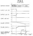
field effect transistor 6 turns off with the inactive low voltage level, and, accordingly, the conduction path between thesense amplifier circuit 5 and the column line DL0 is blocked by the n-channel typefield effect transistor 6. On the other hand, the n-channel type field effect transistor 7 turns on to provide a conduction path between thesense amplifier circuit 5 and the column line DL1, thereby allowing the column line DL1 to be precharged by thesense amplifier circuit 5. The word line WL0 remains in the active high voltage level, so that the column line DL0 continues to be coupled to the ground node, and is discharged to the ground voltage level. As the memory cell M10 is formed by the n-channel type field effect transistor with the relatively high threshold voltage level, the n-channel type field effect transistor keeps off, and, for this reason, the column line DL1 is increased in voltage level toward the high voltage level. If the column line DL1 reaches the high voltage level at time t2, thesense amplifier circuit 5 is activated to increase a small differential voltage level between the column line DL1 and the reference node therein (not shown), thereby deciding that the memory cell M10 memorizes the data bit of logic "1" level. This results in that the output signal of the high voltage level is delivered to the outside thereof. - However, a problem is encountered in the prior art read only memory device in that a relatively long time period is consumed for deciding the logic level of the accessed data bit. This is because of the fact that coupling capacitances C01, C12 and C23 are applied to the adjacent two column lines DL0 and DL1, DL1 and DL2, and DL2 and DL3. Namely, the column line DL1 is affected by the fluctuation in voltage level on the adjacent column line DL0 through the coupling capacitance C01, and, for this reason, the column line DL1 can not be fully charged up to the high voltage level until the column line DL0 reaches the ground level. In other words, the column line DL0 is kept in a voltage level slightly lower than the high voltage level until time t3, and goes up to the high voltage level. If there was no coupling capacitance C01, the column line would reach the high voltage level at time t4, and, for this reason, the time period tc between times t4 and t2 is wasted due to the coupling capacitance C01 between the column lines DL0 and DL1.
- The smaller the gap between the adjacent column line, the larger coupling capacitance, so that the problem is serious in a semiconductor memory device increased in the number of memory cells.
- A non-volatile memory device according to the preamble of claim 1 is disclosed in JP-A-58188394.
- EP-A-0060078 discloses a non-volatile memory having plurality of bit line groups, column address selectors for selecting one of the bit line groups and a second selector for selecting a bit line from the selected bit line group.
- It is an object of the invention to provide a read only memory device which is improved in reading-out speed.
- It is another object of the invention to provide a read only memory device which is free from coupling capacitance between adjacent column lines.
- These objects are achieved by a non-volatile memory device as defined in claim 1;
claim 2 is related to a development of the invention. - The features and advantages of a non-volatile memory device according to the present invention will be more clearly understood from the following description taken in conjunction with the accompanying drawings in which:
- Fig. 1 is a circuit diagram showing the arrangement of a prior art read only memory device;
- Fig. 2 is a diagram showing the waveforms of essential signals which appear in the prior art read only memory device;
- Fig. 3 is a circuit diagram showing the arrangement of another read only memory device;
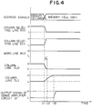
- Fig. 4 is a circuit diagram showing the waveforms of essential signals which appear in the read only memory device shown in Fig. 3;
- Fig. 5 is a diagram showing the arrangement of another read only memory device;
- Fig. 6 is a circuit diagram showing the arrangement of a read only memory device embodying the present invention;
- Fig. 7 is a circuit diagram showing the arrangement of still another read only memory device embodying the present invention;
- Fig. 8 is a diagram showing another read only memory cell alternatively used in the read only memory devices shown in Figs. 3, 5, 6 and 7; and
- Fig. 9 is a diagram showing an electrically erasable read only memory cell capable of being used for formation of the memory cell arrays shown in Figs. 3, 5, 6 and 7.
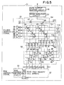
- Referring first to Fig. 3 of the drawings, a read only memory device is fabricated on a
semiconductor substrate 21 and largely comprises amemory cell array 22 coupled to column lines DYO, DY1, DY2, and DY3, a rowaddress decoder circuit 23 coupled to thememory cell array 22 through word lines WL0, WL1, WL2 and WL3, acolumn selector circuit 24, a columnaddress decoder circuit 25 coupled to thecolumn selector circuit 24 through column selecting lines YD0, YD1, YD2 and YD3, a discharging facility 26 provided between thememory cell array 22 and thecolumn selector circuit 24 and coupled to the column selecting lines YD0 to YD3, asense amplifier circuit 27, and a dataoutput buffer circuit 28. - The
memory cell array 22 has a plurality of read only memory cells M00 to M33 arranged in rows and columns, and the read only memory cells M00 to M33 are respectively formed by n-channel type field effect transistors. The n-channel type field effect transistors have respective threshold voltage level of either low or high level, and the low and high threshold voltage levels are about 1.0 volt and about 10.0 volts, respectively. In thememory cell array 22, the n-channel type field effect transistors for the memory cells M00, M11, M12, M23 and M33 are of the low threshold level, however, the other n-channel type field effect transistors have the high threshold voltage level. The n-channel type field effect transistors M00 to M33 of the columns are respectively coupled between the column lines DY0 to DY3 and a constant voltage source or a ground node, and the word lines WL0 to WL3 are shared by the n-channel type field effect transistors M00 to M33 of the rows, respectively. Although only sixteen memory cells are illustrated in Fig. 3, a large number of the memory cells are incorporated in the read only memory device, and, for this reason, a substantial amount of capacitance C01, C12 or C23 is coupled between the adjacent two column lines. - The row
address decoder circuit 23 is well known by a person skilled in the art, so that no detailed description is incorporated for the sake of simplicity. A multiple-bit row address signal is supplied to the rowaddress decoder circuit 23, and the rowaddress decoder circuit 23 selectively shifts the word lines depending upon the row address signal. If one of the word lines WL0 is by way of example selected by the rowaddress decoder circuit 23 and goes up to the active high voltage level, the memory cells M00, M10, M20 and M30 are activated to allow data bits stored therein to be read out to the column lines DL0 to DL3 in the form of voltage level. However, the non-selected word lines remain in the inactive low voltage level, and no data bit is read out from the other memory cells. - The
column selector circuit 24 is provided with a plurality of n-channel typefield effect transistors field effect transistors 29 to 32 are gated by the column selecting lines YD0 to YD3, and one of the n-channel typefield effect transistors 29 to 32 turns on with the active high voltage level to provide a conduction path between one of the column lines and thesense amplifier circuit 27. - The column
address decoder circuit 25 comprises a plurality of series combination circuits each having a NAND gate and an inverter circuit, and is supplied with a multiple-bit column address signal. The address bits of the column address signal and the complementary bits thereof are selectively supplied to the NAND gates, and one of the NAND gates produces the active low voltage level depending upon the bit string of the column address signal. The active low voltage level is inverted at the associated inverter circuit to provide the active high voltage level to the column selecting line. Thus, one of the column selecting lines is shifted to the active high voltage level depending upon the bit string of the column address signal, and, accordingly, associated one of the n-channel type field effect transistors turns on to provide the conduction path for propagating the data bit in the form of voltage level. - The discharging circuit 26 has a plurality of n-channel type
field effect transistors Inverter circuits field effect transistors 33 to 36. The column selecting lines YD0 to YD3 are further coupled to theinverter circuit 37 to 40 for selectively gating the n-channel typefield effect transistors 33 to 36. Both of thecolumn selector circuit 24 and the discharging circuit 26 are formed by the n-channel type field effect transistors, so that the inverter circuit propagating the active high voltage level causes the associated inverter circuit to supply the n-channel type field effect transistor of the discharging circuit 26 with the inactive low voltage level. However, the other column selecting lines remaining in the inactive low voltage level cause the associated inverter circuits to supply the inverter circuits with the active high voltage levels. Thus, the n-channel typefield effect transistors 33 to 36 of the discharging circuit 26 are complementarily shifted between the on-states and the off-states with respect to the n-channel typefield effect transistors 29 to 32 of thecolumn selector circuit 24. - The
sense amplifier circuit 27 is operative to charge up one of the column lines through thecolumn selector circuit 24, and amplifies a small difference in voltage level between the column line propagating a data bit and a reference node (not shown). - Description is hereinbelow made for the operation of the read only memory device with reference to Fig. 4 on the assumption that the memory cell M00 and, thereafter, the memory cell M10 are successively accessed for reading out the data bits stored therein. With the column address signal, the column
address decoder circuit 25 shifts the column selecting line YD0 to the active high voltage level, leaving the other column selecting lines YD1 to YD3 in the inactive low voltage levels. The n-channel typefield effect transistor 29 turns on to allow thesense amplifier circuit 27 to charge up the column line DY0, so that the column line DY0 is increased in voltage level toward the high voltage level of, for example, about 1.5 volt. The active high voltage level is inverted by theinverter circuit 37, and the n-channel typefield effect transistor 33 remains in the off-state with the low voltage level from theinverter circuit 37. On the other hand, the column selecting lines YD1 to YD3 remain in the inactive low voltage level, and, for this reason, no conduction path is established for the other n-channel type field effect transistors 30 to 32. The inactive low voltage levels on the respective column selecting lines YD1 to YD3 are inverted to the active high voltage levels by theinverter circuits 38 to 40, so that the n-channel type field effect transistors turn on to provide conduction paths between the column lines DY1 to DY3 and the ground node. Since the non-selected column lines DY1 to DY3 are thus grounded through the discharging circuit 26, no high voltage is left on the non-selected column lines. - The row
address decoder circuit 23 is supplied with the row address signal and produces the active high voltage level which is applied to the word line WL0. Since the n-channel type field effect transistor for the memory cell M00 has the relatively low threshold voltage level, the n-channel type field effect transistor turns on to provide a conduction path from the column line DL0 to the ground node. This results in that the column line DL0 is slightly discharged to a voltage level of, for example, 1.4 volt, and thesense amplifier circuit 5 decides that the data bit read out from the memory cell M00 is logic "0" level. Though not shown in the drawings, the n-channel typefield effect transistors 31 and 32 remain in the off-states, and the n-channel typefield effect transistors - Next, the column address signal is changed for access to the memory cell M10 at time t11, and, accordingly, the column selecting line YD0 is recovered to the inactive low voltage level, however, the column selecting line YD1 goes up to the active high voltage level. The n-channel type
field effect transistor 29 turns off with the inactive low voltage level, and, accordingly, the conduction path between thesense amplifier circuit 27 and the column line DL0 is blocked by the n-channel typefield effect transistor 29. The inactive low voltage level on the column selecting line YD0 is inverted to the active high voltage level by theinverter circuit 37, and the active high voltage level allows the n-channel typefield effect transistor 33 to turn on. Then, the column line DY0 is rapidly discharged and, accordingly, reaches the ground voltage level at time t12. The time period tc′ between times t11 and t12 is surely reduced by virtue of the discharging circuit 26. - On the other hand, the n-channel type field effect transistor 30 turns on to provide a conduction path between the
sense amplifier circuit 27 and the column line DL1 with the active high voltage level supplied from the columnaddress decoder circuit 25, thereby allowing the column line DL1 to be precharged by thesense amplifier circuit 27. Theinverter circuit 38 produces the inactive low voltage level, so that the n-channel typefield effect transistor 34 turns off to block the conduction path between the column line DY1 and the ground node. The word line WL0 remains in the active high voltage level, so that the column line DL0 continues to be connected to the ground node. Since the memory cell M10 is formed by the n-channel type field effect transistor with the relatively high threshold voltage level, the n-channel type field effect transistor keeps off, and, for this reason, the column line DL1 is rapidly increased toward the high voltage level, because the column line DY0 has been already discharged to the ground level. If the column line DL1 reaches the high voltage level attime 13, thesense amplifier circuit 27 decides that the data bit read out from the memory cell M10 is logic "1" level, and shifts the output signal thereof to the high voltage level. - Turning to Fig. 5, another read only memory device is fabricated on a
semiconductor substrate 51 and largely comprises two read onlymemory cell arrays 52 coupled to column lines DY0, DY1, DY2 and DY3, and DY4, DY5 DY6 and DY7, respectively, a rowaddress decoder circuit 53 coupled to thememory cell array 52 through word lines WL0, WL1, WL2 and WL3, acolumn selector circuit 54, a columnaddress decoder circuit 55 coupled to thecolumn selector circuit 54 through column selecting lines YD0, YD1, YD2 and YD3 as cell as group selecting lines GY0 and GY1, a dischargingfacility 56 provided between thememory cell array 52 and thecolumn selector circuit 54 and coupled to the column selecting lines YD0 to YD7, a sense amplifier circuit 57, and a dataoutput buffer circuit 58. - The word lines WL0 to WL3 are shared by the two read only
memory cell arrays 52, and thecolumn selector circuit 54 is formed in a two-stage configuration. Namely, two groups of n-channel typefield effect transistors column selector circuit 54, and two n-channel typefield effect transistors column selector circuit 54. Thecolumn decoder circuit 55 selectively shifts not only the column selecting lines YD0 to YD3 but also the group selecting lines GY0 and GY1. When one of the column selecting lines YD0 to YD3 goes up to the high voltage level, one of the n-channel typefield effect transistors 59 to 62 turns on, and another n-channel type field effect transistor is selected from the second group of the n-channel typefield effect transistors 63 to 66. For this reason, two conduction paths are established in the first stage of thecolumn selector circuit 54. Thecolumn decoder circuit 55 further shifts one of the group selecting lines GY0 and GY1, so that one of the n-channel typefield effect transistors column selector circuit 54, and, accordingly, one of the column lines DY0 to DY7 is charged up by the sense amplifier circuit 57 for reading out a data bit from the accessed memory cell. - Since the
column selector circuit 54 is of the two stage arrangement, the dischargingcircuit 56 is also formed with two groups of discharging transistors respectively formed by n-channel typefield effect transistors 67 to 82. The n-channel typefield effect transistors 67 to 74 of the first stage are further divided into two sub-groups, and the first and second sub-groups are associated with two column line groups DY0 to DY3 and DY4 to DY7. The n-channel type field effect transistors of the first sub-group are gated by the complementary signal produced by an inverter circuit 83, and are complementarily shifted between on-states and off-states with respect to the n-channel typefield effect transistor 67. Similarly, the n-channel typefield effect transistors 71 to 74 of the second sub-group are simultaneously gated by aninverter circuit 84, and are established into the opposite states with respect to the n-channel typefield effect transistor 68. Thus, one of the column line groups is directly conducted to the ground node. The n-channel typefield effect transistors 75 to 82 of the second group are also divided into two sub-groups, and are gated byinverter circuits 85 to 88 which are coupled to the column selecting lines YD0 to YD3, respectively. This arrangement results in that two of the n-channel typefield effect transistors 75 to 82 are complementary shifted between the on-states and the off-states with respect to the associated n-channel typefield effect transistors 59 to 66, so that two column lines are blocked from the ground node by the two n-channel type field effect transistors of the second group. However, one of the two column lines is conducted to the ground node through one of the sub-groups of the n-channel typefield effect transistors 67 to 74. For this reason, only one column line is isolated from the ground node and propagates the data bit read out from the accessed memory cell in the form of voltage level. - The other circuit arrangements and the behaviors thereof are similar to those of the read only memory device shown in Fig. 3, and, for this reason, no further description is hereinbelow incorporated.
- Turning to Fig. 6, another read only memory device is fabricated on a
semiconductor substrate 91 and largely comprises a read onlymemory cell array 92 coupled to column lines DY0, DY1, DY2 and DY3, respectively, a rowaddress decoder circuit 93 coupled to thememory cell array 92 through word lines WL0, WL1, WL2 and WL3, acolumn selector circuit 94, a columnaddress decoder circuit 95 coupled to thecolumn selector circuit 94 through column selecting lines YD0, YD1, YD2 and YD3, a dischargingfacility 96 provided between thememory cell array 92 and thecolumn selector circuit 94 and supplied with the row address bits a0 and a1 and the complementary bits thereof, asense amplifier circuit 97, and a dataoutput buffer circuit 98. - The discharging
circuits 96 comprises n-channel type field effect transistors 99 to 105 grouped by two, and every two n-channel type field effect transistors are coupled in parallel to every column lines DY0 to DY3. The row address bits a0 and a1 and the complementary bits thereof are selectively supplied to the n-channel type field effect transistors 99 to 106 in such a manner as to be complementarily shifted between on-states and off-states with respect to associated n-channel typefield effect transistors 107 to 110 of thecolumn selector circuit 94. For example, if both of the row address bits a0 and a1 are logic "1" level, the n-channel typefield effect transistor 107 turns on to charge up the column line DY0, and the row address bits of logic "1" level allows the n-channel typefield effect transistors field effect transistors 107 to 110 for discharging the column lines except for that coupled to the accessed memory cell. - The other component circuits and the behaviors thereof are similar to those shown in Fig. 3, so that detailed description is omitted for the sake of simplicity.
- Turning to Fig. 7, another read only memory device is fabricated on a semiconductor substrate 121 and largely comprises a read only
memory cell array 122 coupled to column lines DY0, DY1, DY2 DY3, DY4, DY5 DY6 and DY7, respectively, a rowaddress decoder circuit 123 coupled to thememory cell array 122 through word lines, acolumn selector circuit 124, a columnaddress decoder circuit 125 coupled to thecolumn selector circuit 124 through column selecting lines YD0, YD1, YD2, YD3, YD4, YD5, YD6 and YD7, a dischargingfacility 126 provided between thememory cell array 122 and thecolumn selector circuit 124, a sense amplifier circuit 127, and a dataoutput buffer circuit 128. - The
column selector circuit 124 has a plurality of n-channel typefield effect transistors 129 to 136 selectively gated by the column selecting lines YD0 to YD7, and the dischargingcircuit 126 is formed with two groups of discharging transistors respectively formed by n-channel typefield effect transistors 137 to 152. The n-channel typefield effect transistors 145 to 152 of the first stage are further divided into two sub-groups, and the first and second sub-groups are associated with two column line groups DY0 to DY3 and DY4 to DY7. The n-channel type field effect transistors of the first sub-group are gated by the row address bit a2 and the complementary bit supplied frominverter circuits - The n-channel type
field effect transistors 137 to 144 of the second group are also divided into two sub-groups, and are gated byNAND gates 155 to 158 which are selectively supplied with the row address bits aO and al and the complementary bits thereof. One of theNAND gates 155 to 158 produces the inactive low voltage level, so that only two n-channel type field effect transistors turn off to isolate the column lines coupled to the memory cells specified by the row address signal. Thus, only one current path is established from the sense amplifier circuit 127 to one of the column lines DY0 to DY7 which is isolated from the ground node, however, the other column lines are connected to the ground node through two-stage discharging circuit 126. - The other circuit arrangements and the behaviors thereof are similar to those of the read only memory device shown in Fig. 3, and, for this reason, no further description is hereinbelow incorporated. The discharging
circuit 126 shown in Fig. 7 has the two-stage arrangement, and, for this reason, the signal lines passing therethrough are decreased in number in comparison with a single stage arrangement. - Modifications are possible, for example, each of the memory cells incorporated in the above mentioned read only memory devices is formed of a single n-channel type enhancement-mode field effect transistor, however, the memory cell may be implemented by a series of n-channel type enhancement-mode
field effect transistors 201 to 203 as shown in Fig. 8. The series of the n-channel typefield effect transistors 201 to 203 achieve a NAND operation. Moreover, the memory cell array may be formed by electrically erasable read only memory cells, and each of the electrically erasable read only memory cell can be implemented by a floating gate type MOSfield effect transistor 204 shown in Fig. 9.
Claims (2)
- A non-volatile memory device fabricated on a semiconductor substrate, comprising:a) a plurality of non-volatile memory cells arranged in rows and columns and coupled in parallel to a constant voltage source, said non-volatile memory cells respectively having threshold voltage levels of either high or low level depending upon data bits memorized therein,b) a plurality of word lines (WL0 - WL3) coupled to the rows of said non-volatile memory cells, respectively, and selectively driven to an active level for simultanously reading out the data bits from the memory cells of one of said rows,c) a row address decoder circuit (93, 123) supplied with a row address signal and selectively driving one of said word lines to said active level,d) a plurality of column lines (DY0 - DY3; DY0 - DY7) coupled to said non-volatile memory cells of the columns for propagating the data bits read out form said memory cells in the form of voltage level,e) a column selector circuit (94, 124) coupled to said column lines and activated so as to provide a conduction path for one of said column lines,f) a column address decoder circuit (95, 125) supplied with a column address signal for causing said column selector circuit to select one of said plurality of column lines,g) a sense amplifier circuit (97, 127) for receiving the data bit in the form of voltage level and to decide the logic level of the data bit received,h) a discharging circuit (96, 126) coupled between said column lines and said constant voltage source,characterized in that said sense amplifier is operative to charge said one of said column lines through the column selector circuit and
that said discharging circuit (96) comprises a plurality of switching transistors selectively coupled between said plurality of column lines and said constant voltage source and responsive to said column address signal for discharging at least the column lines adjacent to said one of said column lines. - A non-volatile memory device as claimed in claim 1,
characterized
in that said plurality of column lines is divided into a plurality of column line groups, that an auxiliary column address decoder unit (153 - 158) is provided responsive to said column address signal for producing a column address decoded signal having first signals and second signals, and in that said discharging circuit (126) comprises a plurality of first transistor groups (145 - 148; 149 - 152) respectively associated with said plurality of column line groups and responsive to said first signals so as to select one of said plurality of column line groups, and a plurality of second transistor groups (137 - 140; 141 - 144) respectively associated with said plurality of column lines and each having a plurality of switching transistors gated with said second signals for coupling column lines selected from said one of said plurality of column line groups and adjacent to said one of said column lines with said constant voltage source.
Applications Claiming Priority (2)
| Application Number | Priority Date | Filing Date | Title |
|---|---|---|---|
| JP63158748A JPH029098A (en) | 1988-06-27 | 1988-06-27 | Read-only semiconductor storage device |
| JP158748/88 | 1988-06-27 |
Publications (3)
| Publication Number | Publication Date |
|---|---|
| EP0348893A2 EP0348893A2 (en) | 1990-01-03 |
| EP0348893A3 EP0348893A3 (en) | 1990-08-22 |
| EP0348893B1 true EP0348893B1 (en) | 1995-12-06 |
Family
ID=15678471
Family Applications (1)
| Application Number | Title | Priority Date | Filing Date |
|---|---|---|---|
| EP89111676A Expired - Lifetime EP0348893B1 (en) | 1988-06-27 | 1989-06-27 | High speed non-volatile memory device |
Country Status (3)
| Country | Link |
|---|---|
| EP (1) | EP0348893B1 (en) |
| JP (1) | JPH029098A (en) |
| DE (1) | DE68925001T2 (en) |
Families Citing this family (4)
| Publication number | Priority date | Publication date | Assignee | Title |
|---|---|---|---|---|
| JP2504150B2 (en) * | 1988-12-24 | 1996-06-05 | 三菱電機株式会社 | Semiconductor integrated circuit |
| JPH03283200A (en) * | 1990-03-30 | 1991-12-13 | Toshiba Corp | Non-volatile semiconductor storage device |
| JP2692395B2 (en) * | 1991-01-29 | 1997-12-17 | 日本電気株式会社 | High speed read semiconductor memory device |
| US10134475B2 (en) * | 2015-03-31 | 2018-11-20 | Silicon Storage Technology, Inc. | Method and apparatus for inhibiting the programming of unselected bitlines in a flash memory system |
Citations (1)
| Publication number | Priority date | Publication date | Assignee | Title |
|---|---|---|---|---|
| EP0060078A2 (en) * | 1981-03-06 | 1982-09-15 | Fujitsu Limited | Read-only memory device |
Family Cites Families (5)
| Publication number | Priority date | Publication date | Assignee | Title |
|---|---|---|---|---|
| US4264828A (en) * | 1978-11-27 | 1981-04-28 | Intel Corporation | MOS Static decoding circuit |
| US4340943A (en) * | 1979-05-31 | 1982-07-20 | Tokyo Shibaura Denki Kabushiki Kaisha | Memory device utilizing MOS FETs |
| JPS5740798A (en) * | 1980-08-20 | 1982-03-06 | Matsushita Electric Ind Co Ltd | Read-only storage device |
| JPS5873097A (en) * | 1981-10-27 | 1983-05-02 | Nec Corp | Decoder circuit |
| JPS6137715A (en) * | 1984-07-30 | 1986-02-22 | Kanebo Ltd | Makeup cosmetic |
-
1988
- 1988-06-27 JP JP63158748A patent/JPH029098A/en active Pending
-
1989
- 1989-06-27 EP EP89111676A patent/EP0348893B1/en not_active Expired - Lifetime
- 1989-06-27 DE DE1989625001 patent/DE68925001T2/en not_active Expired - Fee Related
Patent Citations (1)
| Publication number | Priority date | Publication date | Assignee | Title |
|---|---|---|---|---|
| EP0060078A2 (en) * | 1981-03-06 | 1982-09-15 | Fujitsu Limited | Read-only memory device |
Also Published As
| Publication number | Publication date |
|---|---|
| JPH029098A (en) | 1990-01-12 |
| EP0348893A3 (en) | 1990-08-22 |
| EP0348893A2 (en) | 1990-01-03 |
| DE68925001D1 (en) | 1996-01-18 |
| DE68925001T2 (en) | 1996-07-04 |
Similar Documents
| Publication | Publication Date | Title |
|---|---|---|
| US5453955A (en) | Non-volatile semiconductor memory device | |
| EP0477369B1 (en) | Semiconductor memory device | |
| US5959882A (en) | Nonvolatile semiconductor memory device and data writing method therefor | |
| US4377857A (en) | Electrically erasable programmable read-only memory | |
| US6351415B1 (en) | Symmetrical non-volatile memory array architecture without neighbor effect | |
| US5825205A (en) | Level-shift circuit for driving word lines of negative gate erasable type flash memory | |
| KR100308480B1 (en) | Flash memory device with row decoding structure which is appropriate for high desitty | |
| US6256216B1 (en) | Cam array with minimum cell size | |
| US5287310A (en) | Memory with I/O mappable redundant columns | |
| EP0918335A2 (en) | Content-addressable memory | |
| US5023837A (en) | Bitline segmentation in logic arrays | |
| US6005790A (en) | Floating gate content addressable memory | |
| US5274597A (en) | Semiconductor memory device capable of driving divided word lines at high speed | |
| US6028813A (en) | NOR type semiconductor memory device and a method for reading data stored therein | |
| EP0459794B1 (en) | Read only memory device | |
| US7352645B2 (en) | Memory device | |
| US20030202374A1 (en) | Semiconductor memory device | |
| US5402382A (en) | Nonvolatile semiconductor memory device capable of erasing by a word line unit | |
| US6320785B1 (en) | Nonvolatile semiconductor memory device and data writing method therefor | |
| US5229968A (en) | Nonvolatile semiconductor memory wherein dummy cells are used for generating a potential for detecting data | |
| US4602355A (en) | Memory circuit with noise preventing means for word lines | |
| US6683808B2 (en) | String programmable nonvolatile memory with NOR architecture | |
| EP0348893B1 (en) | High speed non-volatile memory device | |
| US4610002A (en) | Dynamic memory circuit with improved noise-prevention circuit arrangement for word lines | |
| US5835421A (en) | Method and apparatus for reducing failures due to bit line coupling and reducing power consumption in a memory |
Legal Events
| Date | Code | Title | Description |
|---|---|---|---|
| PUAI | Public reference made under article 153(3) epc to a published international application that has entered the european phase |
Free format text: ORIGINAL CODE: 0009012 |
|
| 17P | Request for examination filed |
Effective date: 19890627 |
|
| AK | Designated contracting states |
Kind code of ref document: A2 Designated state(s): DE FR GB |
|
| PUAL | Search report despatched |
Free format text: ORIGINAL CODE: 0009013 |
|
| AK | Designated contracting states |
Kind code of ref document: A3 Designated state(s): DE FR GB |
|
| 17Q | First examination report despatched |
Effective date: 19930224 |
|
| GRAA | (expected) grant |
Free format text: ORIGINAL CODE: 0009210 |
|
| AK | Designated contracting states |
Kind code of ref document: B1 Designated state(s): DE FR GB |
|
| RAP1 | Party data changed (applicant data changed or rights of an application transferred) |
Owner name: NEC CORPORATION |
|
| REF | Corresponds to: |
Ref document number: 68925001 Country of ref document: DE Date of ref document: 19960118 |
|
| ET | Fr: translation filed | ||
| PLBE | No opposition filed within time limit |
Free format text: ORIGINAL CODE: 0009261 |
|
| STAA | Information on the status of an ep patent application or granted ep patent |
Free format text: STATUS: NO OPPOSITION FILED WITHIN TIME LIMIT |
|
| 26N | No opposition filed | ||
| REG | Reference to a national code |
Ref country code: GB Ref legal event code: IF02 |
|
| REG | Reference to a national code |
Ref country code: GB Ref legal event code: 732E |
|
| REG | Reference to a national code |
Ref country code: FR Ref legal event code: TP |
|
| PGFP | Annual fee paid to national office [announced via postgrant information from national office to epo] |
Ref country code: FR Payment date: 20050608 Year of fee payment: 17 |
|
| PGFP | Annual fee paid to national office [announced via postgrant information from national office to epo] |
Ref country code: GB Payment date: 20050622 Year of fee payment: 17 |
|
| PGFP | Annual fee paid to national office [announced via postgrant information from national office to epo] |
Ref country code: DE Payment date: 20050623 Year of fee payment: 17 |
|
| PG25 | Lapsed in a contracting state [announced via postgrant information from national office to epo] |
Ref country code: GB Free format text: LAPSE BECAUSE OF NON-PAYMENT OF DUE FEES Effective date: 20060627 |
|
| PG25 | Lapsed in a contracting state [announced via postgrant information from national office to epo] |
Ref country code: DE Free format text: LAPSE BECAUSE OF NON-PAYMENT OF DUE FEES Effective date: 20070103 |
|
| GBPC | Gb: european patent ceased through non-payment of renewal fee |
Effective date: 20060627 |
|
| REG | Reference to a national code |
Ref country code: FR Ref legal event code: ST Effective date: 20070228 |
|
| PG25 | Lapsed in a contracting state [announced via postgrant information from national office to epo] |
Ref country code: FR Free format text: LAPSE BECAUSE OF NON-PAYMENT OF DUE FEES Effective date: 20060630 |