EP0348701A1 - Device for distance measurement - Google Patents
Device for distance measurement Download PDFInfo
- Publication number
- EP0348701A1 EP0348701A1 EP89110254A EP89110254A EP0348701A1 EP 0348701 A1 EP0348701 A1 EP 0348701A1 EP 89110254 A EP89110254 A EP 89110254A EP 89110254 A EP89110254 A EP 89110254A EP 0348701 A1 EP0348701 A1 EP 0348701A1
- Authority
- EP
- European Patent Office
- Prior art keywords
- coil
- signal
- direct current
- frequency
- temperature
- Prior art date
- Legal status (The legal status is an assumption and is not a legal conclusion. Google has not performed a legal analysis and makes no representation as to the accuracy of the status listed.)
- Granted
Links
Images

Classifications
-
- G—PHYSICS
- G01—MEASURING; TESTING
- G01B—MEASURING LENGTH, THICKNESS OR SIMILAR LINEAR DIMENSIONS; MEASURING ANGLES; MEASURING AREAS; MEASURING IRREGULARITIES OF SURFACES OR CONTOURS
- G01B7/00—Measuring arrangements characterised by the use of electric or magnetic techniques
- G01B7/02—Measuring arrangements characterised by the use of electric or magnetic techniques for measuring length, width or thickness
- G01B7/023—Measuring arrangements characterised by the use of electric or magnetic techniques for measuring length, width or thickness for measuring distance between sensor and object
-
- G—PHYSICS
- G01—MEASURING; TESTING
- G01D—MEASURING NOT SPECIALLY ADAPTED FOR A SPECIFIC VARIABLE; ARRANGEMENTS FOR MEASURING TWO OR MORE VARIABLES NOT COVERED IN A SINGLE OTHER SUBCLASS; TARIFF METERING APPARATUS; MEASURING OR TESTING NOT OTHERWISE PROVIDED FOR
- G01D3/00—Indicating or recording apparatus with provision for the special purposes referred to in the subgroups
- G01D3/028—Indicating or recording apparatus with provision for the special purposes referred to in the subgroups mitigating undesired influences, e.g. temperature, pressure
- G01D3/036—Indicating or recording apparatus with provision for the special purposes referred to in the subgroups mitigating undesired influences, e.g. temperature, pressure on measuring arrangements themselves
Definitions
- the invention relates to a device for measuring the distance specified in the preamble of claim 1.
- the coil is usually the resonant circuit coil of a high-frequency oscillator, and it supplies the high-frequency signal dependent on its damping.
- the damping is based on the effective resistance of the coil, which is partly due to the eddy current losses in the object, which affect the coil, and moreover is caused by the DC resistance of the coil, which depends on the temperature of the coil.
- the advantage of distance measurement with devices of the type in question is that it is sufficient to arrange only the coil at the measurement location, while the oscillator and the evaluation circuit can be operated at a certain distance from the measurement location, in particular at room temperature, while the coil at a higher location (or lower) temperature at which other parts of the device could not operate, especially if they are equipped with semiconductor elements.
- the influence of temperature on the amount of damping caused by the DC resistance of the coil is no longer negligible, so that the high-frequency signal depends on both the distance of the object from the coil and the temperature of the coil depends.
- the DC resistance of the coil increases approximately twice when the temperature increases by 250 ° C.
- the DC voltage signal can be obtained as a voltage drop in a constant DC current flowing through the coil.
- the object is achieved to provide a device for distance measurement with improved temperature compensation.
- the energy lost in the temperature-dependent direct current resistance of the coil is always covered by the correspondingly temperature-controlled high-frequency current source, so that the alternating magnetic field generated by the coil is independent of the temperature.
- the device has four switches which are jointly controlled by a clock generator and a measuring head which in any case contains the coil and has four connections, the second and fourth of which are grounded. When the switches are in one position, the first connection is connected to an oscillator and the third connection is connected via an amplifier, rectifier and a logarithmic element to a holding circuit controlled by the clock generator, which supplies the distance signal.
- the third measuring head connection is connected instead of to the amplifier to a direct current source which supplies a constant direct current and which prevails at this third measuring head connection the coil temperature dependent DC voltage is at the input of a circuit that supplies a signal to the oscillator.
- the measuring head is neither connected to the oscillator nor to the amplifier and the logarithmic element is not connected to the holding circuit either, and when the switch is switched back to its first position the DC source is switched off and also the input of the circuit supplying the signal to the oscillator is grounded, the oscillator oscillates exactly as before and the distance signal is not temperature compensated.
- the magnetic, high-frequency alternating field of the coil is independent of the temperature.
- the damping of the coil is always influenced by the object under the same conditions, and a high-frequency signal is generated which only depends on the distance of the object from the coil.
- the device With the device, a signal dependent on the distance a of an object 1 from a high-frequency excited coil L1 is generated.
- the object 1 is arranged on an end face of the coil L1 and, if it is not itself electrically (or magnetically) conductive, is provided with a coating (not shown) of these properties.
- the coil L1 is the resonant circuit coil of a high-frequency oscillator 5
- the High-frequency voltage is on a line 7 to which a diode D1 with subsequent smoothing element 12 is connected.
- the output voltage of the smoothing element 12 is a signal dependent on the distance a.
- the damping of the resonant circuit also depends on the DC resistance of coil L1, which is temperature-dependent.
- the output voltage of the filter element 12 also depends on the temperature of the coil L1.
- a direct current from a constant current source 9 is superimposed on the high-frequency current flowing through the coil L1, and the voltage drop of the direct current at the coil L1 is input to a control circuit 10, 6 which controls the Controls the oscillating DC current depending on the DC voltage drop and thus counteracts temperature-related changes in the high-frequency voltage.
- the constant current source 9 is connected to the line 7 by a high-frequency choke coil L2, which keeps the high frequency away from the constant current source 9, and the control circuit has an inverting amplifier 10, a resistor network 14 and a controllable current source 6, which feed the oscillator 5 DC supplies.
- the input of amplifier 10 is through a radio frequency block forming RC element R1, C1 connected to line 7, the output voltage of which is at the input of resistance network 14, the output of which is connected to the control input of current source 6.
- the DC voltage drop across coil L1 which is at the input of amplifier 10, increases.
- the output voltage and thus the control voltage of the controllable current source 6 increases and an amplifier 04 (FIG.
- the network 14 ensures that the amount by which the control circuit 10, 14, 6 changes the high-frequency excitation of the coil L1 when the temperature thereof changes is equal to the amount which the excitation would change if the control circuit 10, 14, 6 were not present. As a result, the influence of the temperature of the coil L1 on its high-frequency excitation is compensated, so that the high-frequency voltage and the signal corresponding to this voltage at the output of the filter element 12 only depend on the distance of the object 1 from the coil L1.
- the current source 6 which feeds the oscillator 5 is controlled to compensate for the temperature dependence of the direct current resistance of the coil L1 by the signal at the output of the amplifier 10 which is dependent thereon.
- the dependence of the high-frequency voltage on the coil L1 on the distance a is not linear. This high-frequency voltage increases steeply with increasing distance a and then gradually less steeply.
- a signal which depends practically linearly on the distance a can be obtained from the high-frequency voltage rectified by means of the diode D1 and smoothed in the smoothing element 12 by a non-linear transmission element, the output voltage of which first increases less steeply and then steeply with increasing input voltage.
- Semiconductor components with a barrier layer, in particular diodes, are known to have a current-voltage characteristic which rises less steeply in the region of small voltages with increasing voltage and then rises more steeply.
- a non-linear transmission element 15 for the rectified and smoothed high-frequency voltage can thus be obtained, which delivers a signal whose dependence on the distance a is linear.
- a non-linear element 15 of a special type which is described in more detail below and in which the temperature dependency of the diode characteristic is compensated, is provided, which works together with an amplifier 16 which produces the desired signal delivers at the output 17 of the circuit arrangement.
- the dependence of this signal on the distance a is linear, and the signal is, as previously explained, independent of the temperature of the coil L1, and the influence of the temperature on the diode characteristic that is decisive for the linearization is compensated, as will be explained further below .
- the power supply to the circuit parts 5, 6, 9, 10, 12, 13, 14, 15 and 16 takes place on a line 19 with e.g. 17.2 volts and a line 20 with e.g. 6.3 volts based on ground 22.
- These voltages are stabilized in a manner known per se by means of a Darlington circuit T1, T2, a differential amplifier O1 and two Zener diodes Z1 and Z2.
- the high-frequency oscillator 5 is a Colpitts oscillator in the basic circuit with a transistor T4 and the resonant circuit formed by the coil L1 and two capacitors C2 and C3, which is connected on the one hand to the collector of the transistor T4 and the high-frequency line 7 and on the other hand to ground 22 lies.
- the smoothing element 12 contains, in a known manner, two capacitors C6, C7 and a resistor K1, which is designed to compensate for the effects of temperature on the circuit arrangement (without coil L1), in particular the semiconductor diode D1, as a PTC thermistor for smoothing high frequency.
- the constant current source 9 is implemented in a known manner with an operational amplifier O2, a transistor T5 in a collector circuit and five resistors R9 to R13. It supplies the constant direct current to the high-frequency end of coil L1 connected to line 7. This current is e.g. dimensioned so that the DC voltage drop across coil L1 at room temperature is approximately 0.2 volts.
- the collector current of the transistor T4 which also flows through the coil L1 and inevitably changes with the distance a, is of no importance.
- the current flowing through the resistors R1, R16, R19, R20 / 21 and the coil L1 is negligible, it is also stabilized because of the stabilized voltage on the line 19, albeit with greater deviations than the current of the Constant current source 9, which in turn is fed with this voltage.
- the controllable current source 6 contains as an actuator for the direct current supply of the oscillator 5 an operational amplifier O4 and resistors R24 to R29.
- the output voltage of the resistor network 14 is the manipulated variable at the input of the operational amplifier O4.
- the amplifier 13 is an operational amplifier O5, the non-inverting input of which is connected to the output of the filter element 12 by a resistor R 36 and the inverting input of which is fed by a voltage divider R 32, R 33.
- the resistor network 14 contains a resistor 23, which connects the output of the amplifier 10 to the control input of the current source 6, which also has a resistor was upstream of R24.
- Resistors 28 and 42 provide the required bias at the inverting input of amplifier O4.
- the resistors R23 and R42, together with the resistor R28, cause the voltage at the control input of the current source 6, which is dependent on the temperature of the coil L1, to be as great as is necessary for the most complete possible compensation.
- the described compensation of the influence of the temperature on the high-frequency voltage of the coil L1 by the temperature-dependent direct current resistance of the coil L1 is no longer sufficient, as has been shown, when the coil L1 is exposed to extreme temperatures, for example 24 o K or 300 o C. Then come additional, other temperature-dependent influences on the damping and thus on the high-frequency voltage of the coil L1. For example, it could be dielectric losses in the insulation of the coil wire or eddy current losses in the coil body (not shown). In order to also take these additional effects into account in the intended temperature compensation, the measuring head 23 containing the coil can be equipped with a network D3, R60, C12 according to FIG. 4.
- the suitable network and its elements, in particular the type of diode D1 and the resistance value and the (temperature-dependent) material of the resistor R60 or R61 can be determined by tests.
- the resistance value of R60 or R61 should not be more than 5%, at most 10%, of the DC resistance of coil L1.
- the capacitor C12 or C13 is to be dimensioned such that its impedance is negligible at the frequency in question bar is small compared to the resistance of the series circuit D1, R60 or to the resistor R61. Its capacity must be a multiple of the capacity of C2 and C3. As can be seen from FIGS.
- the additional network D5, R60, C12 and R61 C13 is connected in series with the coil L1, so that the measuring head also has only two connections in this embodiment, and the compensation with a single DC voltage takes place, ie the direct current source 6 of the oscillator 5 is only controlled by a direct voltage containing all temperature-related influences.
- a voltage that only depends on the DC resistance and a voltage determined by the network could act on the DC source 6.
- the non-linear element 15 contains two branches connected in parallel, each of which consists of a transistor T6 or T7 connected as a diode in series with a resistor R49 or R50. Transistors are used because such a pair is commercially available in a package on a semiconductor substrate that maintains both transistors at the same temperature, and as described below, such a pair is required for temperature compensation of an electrical signal.
- the branches T6, R49 and T7, R50 are in FIG. 2 at the output of an operational amplifier O6, whose non-inverting input is connected to line 20, and whose inverting input is connected to the base and the collector of transistor T7.
- This operational amplifier 06 is fundamentally not necessary, it only brings about a further improvement in the action of the non-linear element 15.
- the mode of operation of an embodiment is therefore described in which the branches T6, R49 and T7, R50 are connected directly to line 20 (without an operational amplifier) are.
- the transistors T6 and T7 have the same characteristics and in the quiescent state there are equal voltage drops across the resistors R 49 and 50, so that in the quiescent state the voltages across the transistors T6 and T7 are equal to one another.
- the output of amplifier 13 is connected through a resistor 44 to the end of resistor 49 connected to the base and collector of transistor T6, so that the output voltage of this amplifier 13 increases the voltage across this resistor 49.
- the voltage across transistor T6 increases, causing its operating point to shift in terms of its current-voltage characteristic and the current it supplies to resistor R49 to decrease more than proportional to the output voltage of differential amplifier 05 in accordance with the characteristic.
- the current-voltage characteristic of the transistors T6 and T7 connected as diodes is already temperature-dependent in the range of normal room temperatures. This temperature influence is compensated for by the fact that the end of the resistor 49 facing the transistor T6 is connected by a resistor R53 with the non-inverting input and the end of the resistor R50 facing the transistor T7 is connected by a PTC thermistor K2 and a resistor R52 is connected to the inverting input of an operational amplifier O7, the output of which supplies the desired signal, which is linearly dependent on the distance a, at the output 17 of the circuit arrangement. This signal is determined by the difference in the voltages across the resistors R49 and R50.
- the voltage at R49 has arisen from the high-frequency voltage at coil L1 and is linearized with respect to distance a by means of transistor T6.
- the voltage at R50 is an auxiliary voltage (independent of the distance a). Both voltages depend on the temperature of transistors T6 and T7 with a small deviation, so that their difference, that is the linearized output voltage at 17 (apart from the small deviation), is temperature-independent. This deviation arises because the two voltages are unequal, which is why the operating points of the transistors T6 and T7 connected as diodes have their characteristics at different points.
- the PTC thermistor K2 is used to compensate for this deviation.
Abstract
Die Dämpfung einer Spule (L1) ist von einem Objekt (1) beeinflussbar, so dass die Hochfrequenzspannung an der Spule (L1) vom Abstand (a) des Objekts (1) von der Spule (L1) abhängt. Dem Hochfrequenzstrom durch die Spule ist ein konstanter Gleichstrom überlagert, wobei der Gleichspannungsabfall an der Spule (L1) entsprechend dem die Spule (L1) dämpfenden Gleichstromwiderstand der Spule (L1) von der Temperatur beeinflusst ist. Die hochfrequente Erregung (5, 6) der Spule (L1) ist von dem Gleichspannungsabfall gesteuert, um den Einfluss der Temperatur auf die Hochfrequenzspannung zu kompensieren, so dass die Hochfrequenzspannung nur von dem Abstand (a) abhängt. Die Hochfrequenzspannung, die nichtlienear mit dem Abstand (a) zusammenhängt, ist in einem nichtlinearen Glied (15) mit einem Halbleiterelement in Bezug auf die Entfernung (a) linearisiert. Dabei ist der Einfluss der Temperatur auf die Linearisierung mittels eines zweiten Halbleiterelement kompensiert. 
Description
Die Erfindung bezieht sich auf eine Vorrichtung zur Abstandsmessung der im Oberbegriff des Patentanspruchs 1 angegebenen Gattung.The invention relates to a device for measuring the distance specified in the preamble of
Bei solchen Vorrichtungen ist die Spule üblicherweise die Schwingkreisspule eines Hochfrequenzoszillators, wobei sie das von ihrer Dämpfung abhängige Hochfrequenzsignal liefert. Die Dämpfung beruht auf dem Wirkwiderstand der Spule, der teilsweise durch die Wirbel stromverluste im Objekt, die auf die Spule zurückwirken, und im übrigen durch den Gleichstromwiderstand der Spule verursacht ist, der von der Temperatur der Spule abhängt.In such devices, the coil is usually the resonant circuit coil of a high-frequency oscillator, and it supplies the high-frequency signal dependent on its damping. The damping is based on the effective resistance of the coil, which is partly due to the eddy current losses in the object, which affect the coil, and moreover is caused by the DC resistance of the coil, which depends on the temperature of the coil.
Der Vorteil der Abstandsmessung mit Vorrichtungen vorliegender Gattung besteht wesentlich darin, dass es genügt, am Messort nur die Spule anzuordnen, während der Oszillator und die Auswerteschaltung in einer gewissen Entfernung vom Messort betrieben werden können, insbesondere bei Raumtemperatur, während die Spule am Messort einer höheren (oder tieferen) Temperatur ausgesetzt ist, bei der anderen Teile der Vorrichtung nicht betrieben werden könnten, besonders wenn sie mit Halbleiterelementen ausgerüstet sind.The advantage of distance measurement with devices of the type in question is that it is sufficient to arrange only the coil at the measurement location, while the oscillator and the evaluation circuit can be operated at a certain distance from the measurement location, in particular at room temperature, while the coil at a higher location (or lower) temperature at which other parts of the device could not operate, especially if they are equipped with semiconductor elements.
Bei erheblich von der Raumtemperatur abweichenden Temperaturen ist jedoch der Einfluss der Temperatur auf den Anteil der Dämpfung, der durch den Gleichstromwiderstand der Spule verurscht ist, nicht mehr vernachlässigbar, so dass das Hochfrequenzsignal sowohl vom Abstand des Objekts von der Spule als auch von der Temperatur derselben abhängt. Beispielsweise steigt der Gleichstromwiderstand der Spule bei einer Temperaturerhöhung um 250 °C auf ungefähr das Doppelte.If the temperature deviates significantly from the room temperature, however, the influence of temperature on the amount of damping caused by the DC resistance of the coil is no longer negligible, so that the high-frequency signal depends on both the distance of the object from the coil and the temperature of the coil depends. For example, the DC resistance of the coil increases approximately twice when the temperature increases by 250 ° C.
Um die Abhängigkeit des aus dem Hochfrequenzsignal erhaltenen Abstandssignals von der Temperatur zu vermeiden, wurde vorgeschlagen, mittels einer die Spule speisenden Gleichstromquelle ein von der Spulentemperatur abhängiges Gleichstromsignal zu erzeugen und zur Kompensation des Einflusses der Temperatur auf das Abstandssignal zu verwenden.In order to avoid the dependency of the distance signal obtained from the high-frequency signal on the temperature, it was proposed to generate a direct current signal dependent on the coil temperature using a direct current source feeding the coil and to use it to compensate for the influence of the temperature on the distance signal.
Das Gleichspannungssignal kann als Spannungsabfall eines durch die Spule fliessenden konstanten Gleichstroms erhalten werden.The DC voltage signal can be obtained as a voltage drop in a constant DC current flowing through the coil.
Aus der EP-A-0 049 304 ist eine Vorrichtung dieser Gattung bekannt, bei der ein aus dem Hochfrequenzsignal erhaltenes Signal und ein aus dem Gleichstromsignal erhaltenes Signal einem Summierglied zugeführt sind, welches als Summensignal das Abstandssignal liefert. Wenn bei dieser bekannten Vorrichtung die Temperatur der Spule ändert, ändern sich das Gleichstromsignal und das daraus erhaltene, dem Summierglied zugeführte Signal. Die Folge ist eine entsprechende Aenderung des als Summensignal von dem Summierglied erhaltenen Abstandssignals auch dann, wenn der Abstand der Spule vom Objekt unverändert geblieben ist, d. h. das Abstandssignal ändert sich bei konstantem Abstand mit der Temperatur.From EP-A-0 049 304 a device of this type is known, in which a signal obtained from the high frequency signal and a signal obtained from the direct current signal are fed to a summing element which supplies the distance signal as a sum signal. In this known device, when the temperature of the coil changes, the DC signal and the signal obtained therefrom and fed to the summing element change. The result is a corresponding change in the distance signal obtained as a sum signal from the summing element even if the distance of the coil from the object has remained unchanged, i. H. the distance signal changes with temperature at a constant distance.
Durch die Erfindung, wie sie im Patentanspruch 1 gekennzeichnet ist, wird die Aufgabe gelöst, eine Vorrichtung zur Abstandsmessung mit verbesserter Temperaturkompensation zu schaffen.By the invention, as characterized in
Bei der erfindungsgemässen Vorrichtung wird die im temperaturabhängigen Gleichstromwiderstand der Spule verloren gehende Energie stets aus der entsprechend temperaturgesteuerten Hochfrequenzstromquelle gedeckt, so dass das von der Spule erzeugte magnetische Wechselfeld unabhängig von der Temperatur ist.In the device according to the invention, the energy lost in the temperature-dependent direct current resistance of the coil is always covered by the correspondingly temperature-controlled high-frequency current source, so that the alternating magnetic field generated by the coil is independent of the temperature.
In den Patent Abstracts of Japan, Band 9, Nr. 203 (P-381) (1926), 21. Aug. 1985, ist eine gattungsmässig andere Vorrichtung zur Abstandsmessung beschrieben, die dadurch temperaturkompensiert sein soll, dass ein tem peraturabhängiges Gleichspannungssignal auf den Oszillator wirkt. Jedoch sind die Beschreibung und das Schaltbild auch im Zusammenhang miteinander unverständlich. Die Vorrichtung hat vier von einem Taktgeber gemeinsam gesteuerte Schalter und einen Messkopf, der jedenfalls die Spule enthält und vier Anschlüsse hat, deren zweiter und vierter geerdet sind. In einer Stellung der Schalter ist der erste Anschluss mit einem Oszillator und der dritte Anschluss über einen Verstärker, Gleichrichter und ein Logarithmierglied mit einem vom Taktgeber gesteuerten Haltestromkreis verbunden, der das Abstandssignal liefert. In der anderen Stellung der Schalter ist die Verbindung des Oszillators mit dem ersten Messkopfanschluss und die Verbindung des Logarithmiergliedes mit dem Haltestromkreis unterbrochen, der dritte Messkopfanschluss ist statt mit dem Verstärker mit einer einen konstanten Gleichstrom liefernden Gleichstromquelle verbunden, die an diesem dritten Messkopfanschluss herrschende, von der Spulentemperatur abhängige Gleichspannung liegt am Eingang einer Schaltung, die ein Signal an den Oszillator liefert. Da aber in dieser Schalterstellung der Messkopf weder mit dem Oszillator noch mit dem Verstärker und das Logarithmierglied auch nicht mit dem Haltestromkreis verbunden ist, und beim Zurückschalten der Schalter in ihre erste Stellung die Gleichstromquelle abgeschaltet und ausserdem der Eingang der das Signal an den Oszillator liefernden Schaltung geerdet ist, schwingt der Oszillator genau so wie vorher, und das Abstandssignal ist nicht temperaturkompensiert. Eine Kompensation des Einflusses der Temperatur auf das Abstandssignal ist nicht offenbart. Auch ist diese Vorrichtung bereits gattungsmässig anders als die vorliegende. Bei ihr ist der Gleichstrom in der Spule nicht dem Hochfrequenzstrom überlagert, sondern es fliesst je nach der Stellung der Schalter entweder Hochfrequenz oder Gleichstrom durch die Spule.In the Patent Abstracts of Japan,
Wie weiter oben erwähnt, ist bei der erfindungsgemässen Vorrichtung das magnetische, hochfrequenzte Wechselfeld der Spule unabhängig von derTemperatur. Dabei wird die Dämpfung der Spule durch das Objekt stets unter denselben Bedingungen beeinflusst, und es entsteht ein Hochfreqeuenzsignal, das nur vom Abstand des Objekts von der Spule abhängt.As mentioned above, in the device according to the invention the magnetic, high-frequency alternating field of the coil is independent of the temperature. The damping of the coil is always influenced by the object under the same conditions, and a high-frequency signal is generated which only depends on the distance of the object from the coil.
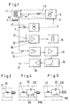
Im folgenden wird die Erfindung einschliesslich besonderer Ausführungsarten anhand der nur einen Ausführungsweg darstellenden, beiliegenden Zeichnungen näher erläutert. Es zeigen:
- Fig. 1 ein Blockdiagramm,
- Fig. 2 das detaillierte Schaltbild einer erfindungsgemässen Vorrichtung und
- Fig. 3 bis 5 je einem Messkopf.
- 1 is a block diagram;
- Fig. 2 shows the detailed circuit diagram of an inventive device and
- 3 to 5 each a measuring head.
Mit der Vorrichtung wird ein vom Abstand a eines Objekts 1 von einer hochfrequent erregten Spule L1 abhängiges Signal erzeugt. Dazu ist das Objekt 1 an einer Stirnseite der Spule L1 angeordnet und, falls es nicht selbst elektrisch (oder magnetisch) leitend ist, mit einem (nicht dargestellten) Belag dieser Eigenschaften versehen. Wie im Prinzip aus Fig. 1 und im einzelnen aus Fig. 2 ersichtlich, ist die Spule L1 die Schwingkreisspule eines Hochfrequenzoszillators 5, dessen Hochfrequenzspannung an einer Leitung 7 liegt, an die eine Diode D1 mit nachfolgendem Glättungsglied 12 angeschlossen ist. Da die Rückwirkung der im Objekt 1 induzierten Wirbelströme auf die Spule L1 die Dämpfung des Oszillator-Schwingkreises in einem vom Abstand a abhängigen Masse erhöht und dadurch dessen Hochfrequenzspannung herabsetzt, ist die Ausgangsspannung des Glättungsgliedes 12 ein von dem Abstand a abhängiges Signal.With the device, a signal dependent on the distance a of an
Die Dämpfung des Schwingkreises hängt auch vom Gleichstromwiderstand der Spule L1 ab, der temperaturabhängig ist. Damit hängt die Ausgangsspannung des Siebgliedes 12 zusätzlich auch von der Temperatur der Spule L1 ab.The damping of the resonant circuit also depends on the DC resistance of coil L1, which is temperature-dependent. Thus, the output voltage of the
Um den Einfluss der Temperatur auf die Ausgangsspannung des Siebgliedes 12 zu kompensieren, ist dem durch die Spule L1 fliessenden Hochfrequenzstrom ein Gleichstrom einer Konstantstromquelle 9 überlagert, und der Spannungsabfall des Gleichstroms an der Spule L1 liegt als Eingangsgrösse an einer Steuerschaltung 10, 6, welche den Oszillator speisenden Gleichstrom in Abhängigkeit von dem Gleichspannungsabfall steuert und dadurch temperaturbedingten Aenderungen der Hochfrequenzspannung entgegenwirkt.In order to compensate for the influence of the temperature on the output voltage of the
Zu diesem Zwecke ist die Konstantstromquelle 9 mit der Leitung 7 durch eine Hochfrequenzdrosselspule L2 verbunden, welche die Hochfrequenz von der Konstantstromquelle 9 fernhält, und die Steuerschaltung weist einen invertierenden Verstärker 10, ein Widerstandsnetzwerk 14 und eine steuerbare Stromquelle 6 auf, die den Oszillator 5 speisenden Gleichstrom liefert. Der Eingang des Verstärkers 10 ist durch ein Hochfrequenzsperre bildendes R-C-Glied R1, C1 mit der Leitung 7 verbunden, dessen Ausgangsspannung am Eingang des Widerstandsnetzwerkes 14 liegt, dessen Ausgang mit dem Steuereingang der Stromquelle 6 verbunden ist. Wenn die Spulentemperatur zunimmt, nimmt der Gleichspannungsabfall an der Spule L1, der am Eingang des Verstärkers 10 liegt, zu. Dabei nimmt dessen Ausgangsspannung und damit die Steuerspannung der steuerbaren Stromquelle 6 zu und ein Verstärker 04 (Fig. 2) der Stromquelle 6, die den Speisegleichstrom des Oszillators 5 liefert, bewirkt eine Erhöhung des Speisestromes und damit der Erregung der Spule L1. Bei einer Abnahme der Spulentemperatur sind die Vorgänge entsprechend umgekehrt. Durch das Netzwerk 14 wird bei im übrigen gegebenen Daten der Schaltungsteile 5, 6, 10 erreicht, dass der Betrag, um den die Steuerschaltung 10, 14, 6 die Hochfrequenzerregung der Spule L1 bei einer Aenderung deren Temperatur ändert, gleich dem Betrag ist, um den die Erregung ändern würde, wenn die Steuerschaltung 10, 14, 6 nicht vorhanden wäre. Im Ergebnis ist der Einfluss der Temperatur der Spule L1 auf deren Hochfrequenzerregung kompensiert, so dass die Hochfrequenzspannung und das dieser Spannung entsprechende Signal am Ausgang des Siebgliedes 12 nur vom Abstand des Objekts 1 von der Spule L1 abhängt.For this purpose, the constant
Auf diese Weise wird die den Oszillator 5 speisende Stromquelle 6 zur Kompensation der Temperaturabhängigkeit des Gleichstromwiderstandes der Spule L1 durch das von diesem abhängige Signal am Ausgang des Verstärkers 10 gesteuert.In this way, the
Wenn der Abstand a bei konstanter Temperatur grösser wird, nimmt die Ausgangsspannung des Glättungsgliedes 12 zu, der Eingang des Verstärkers 13 wird positiver, die Ausgangsspannung des Verstärkers 13 nimmt zu, wodurch der den Oszillator 5 speisende Strom schwächer wird. Im Ergebnis wird ein bei zunehmendem Abstand a zunehmendes Signal an der Ausgangsleitung 17 erhalten, das unabhängig von der Temperatur ist.If the distance a increases at a constant temperature, the output voltage of the
Die Abhängigkeit der Hochfrequenzspannung an der Spule L1 vom Abstand a ist nicht linear. Diese Hochfrequenzspannung nimmt bei zunehmendem Abstand a zuerst steil und dann allmählich immer weniger steil zu.The dependence of the high-frequency voltage on the coil L1 on the distance a is not linear. This high-frequency voltage increases steeply with increasing distance a and then gradually less steeply.
Ein Signal, das praktisch linear vom Abstand a abhängt, kann aus der mittels der Diode D1 gleichgerichteten und im Glättungsglied 12 geglätteten Hochfrequenzspannung durch ein nichtlineares Uebertragungsglied erhalten werden, dessen Ausgangsspannung bei zunehmender Eingangsspannung zuerst weniger steil und dann steiler zunimmt. Halbleiterbauelemente mit Sperrschicht, insbesondere Dioden, haben bekanntlich eine im Bereich kleiner Spannungen mit zunehmender Spannung zuerst weniger steil und dann steiler ansteigende Strom-Spannungs-Charakteristik. Damit kann ein nichtlineares Uebertragungsglied 15 für die gleichgerichtete und geglättete Hochfrequenzspannung erhalten werden, das ein Signal liefert, dessen Abhängigkeit vom Abstand a linear ist.A signal which depends practically linearly on the distance a can be obtained from the high-frequency voltage rectified by means of the diode D1 and smoothed in the
Die Charakteristik einer Diode ist bei Temperaturschwankungen auch im Bereich der Raumtemperaturen, nennenswerten Aenderungen unterworfen. Deshalb ist bei der Schaltungsanordnung nach Fig. 1 und 2 ein nichtlineares Glied 15 besonderer, im folgenden näher beschriebener Art, bei der die Temperaturabhängigkeit der Diodencharakteristik kompensiert ist, vorgesehen, das mit einem Verstärker 16 zusammenarbeitet, der das gewünschte Sig nal am Ausgang 17 der Schaltungsanordnung liefert. Dabei ist die Abhängigkeit dieses Signals vom Abstand a linear, und das Signal ist, wie vorher erläutert, unabhängig von der Temperatur der Spule L1, und auch der Einfluss der Temperatur auf die für die Linearisierung massgebende Diodencharakteristik ist, wie weiter unten noch erläutert, kompensiert.The characteristic of a diode is subject to significant changes in the case of temperature fluctuations, even in the area of room temperatures. Therefore, in the circuit arrangement according to FIGS. 1 and 2, a
Im folgenden werden Einzelheiten der Schaltungsteile der Schaltungsanordnung anhand Fig. 2 näher erläutert.Details of the circuit parts of the circuit arrangement are explained in more detail below with reference to FIG. 2.
Die Stromversorgung der Schaltungsteile 5, 6, 9, 10, 12, 13, 14, 15 und 16 erfolgt an einer Leitung 19 mit z.B. ca. 17,2 Volt und einer Leitung 20 mit z.B. 6,3 Volt bezogen auf Masse 22. Diese Spannungen sind in an sich grundsätzlich bekannter Weise mittels einer Darlingtonschaltung T1, T2, einem Differenzverstärker O1 und zweier Zenerdioden Z1 und Z2 stabilisiert.The power supply to the
Der Hochfrequenzoszillator 5 ist ein Colpitts-Oszillator in Basisschaltung mit einem Transistor T4 und dem durch die Spule L1 und zwei Kondensatoren C2 und C3 gebildeten Schwingkreis, der einerseits mit dem Kollektor des Transistors T4 und der die Hochfrequenz führenden Leitung 7 verbunden ist und andererseits an Masse 22 liegt.The high-
Das Glättungsglied 12 enthält zur Glättung gleichgerichteter Hochfrequenz in bekannter Weise zwei Kondensatoren C6, C7 und einen Widerstand K1, der zur Kompensation von Einflüssen der Temperatur auf die Schaltungsanordnung (ohne Spule L1), insbesondere der Halbleiterdiode D1, als Kaltleiter ausgeführt ist.The
Die Konstantstromquelle 9 ist in bekannter Art mit einem Operationsverstärker O2, einem Transistor T5 in Kollektorschaltung und fünf Widerständen R9 bis R13 ausgeführt. Sie liefert den konstanten Gleichstrom an das Hochfrequenz führende, mit der Leitung 7 verbundene Ende der Spule L1. Dieser Strom ist z.B. so bemessen, dass der Gleichspannungsabfall an der Spule L1 bei Raumtemperatur ca. 0,2 Volt beträgt. Dabei ist der ebenfalls durch die Spule L1 fliessende, mit dem Abstand a zwangsläufig ändernde Kollektorstrom des Transistors T4 unbeachtlich. Auch der durch die Widerstände R1, R16, R19, R20/21 und die Spule L1 fliessende Strom fällt dabei nicht ins Gewicht, er ist im übrigen wegen der stabilisierten Spannung an der Leitung 19 auch stabilisiert, wenn auch mit grösseren Abweichungen als der Strom der Konstantstromquelle 9, die ihrerseits mit dieser Spannung gespeist ist.The constant
Die steuerbare Stromquelle 6 enthält als Stellglied für die Gleichstromversorgung des Oszillators 5 einen Operationsverstärker O4 und Widerstände R24 bis R29. Dabei ist die Ausgangsspannung des Widerstandsnetzwerkes 14 die Stellgrösse am Eingang des Operationsverstärkers O4.The controllable
Der Verstärker 13 ist ein Operationsverstärker O5, dessen nicht invertierender Eingang durch einen Widerstand R 36 mit dem Ausgang des Siebgliedes 12 verbunden und dessen invertierender Eingang von einem Spannungsteiler R 32, R 33 gespeist ist.The
Das Widerstandsnetzwerk 14 enthält einen Widerstand 23, der den Ausgang des Verstärkers 10 mit dem Steuereingang der Stromquelle 6 verbindet, dem noch ein Wider stand R24 vorgeschaltet ist. Durch die Widerstände 28 und 42 wird die erforderliche Vorspannung am invertierenden Eingang des Verstärkers O4 erhalten. Die Widerstände R23 und R42 bewirken zusammen mit dem Widerstand R28, dass die von der Temperatur der Spule L1 abhängige Spannung am Steuereingang der Stromquelle 6 so gross ist, wie für eine möglichst vollständige Kompensation erforderlich.The
Die beschriebene Kompensation des Einflusses der Temperatur auf die Hochfrequenzspannung der Spule L1 durch den temperaturabhängigen Gleichstromwiderstand der Spule L1 genügt, wie sich gezeigt hat, nicht mehr, wenn die Spule L1 extremen Temperaturen ausgesetzt ist, beispielsweise 24 oK oder 300 oC. Dann kommen zusätzliche, andere temperaturabhängige Einflüsse auf die Dämpfung und damit auf die Hochfrequenzspannung der Spule L1 zur Wirkung. Beispielsweise könnte es sich um dielektrische Verluste in der Isolation des Spulendrahtes oder um Wirbelstromverluste im (nicht dargestellten) Spulenkörper handeln. Um auch diese zusätzlichen Wirkungen bei der beabsichtigten Temperaturkompensation zu berücksichtigen, kann der die Spule enthaltende Messkopf 23 mit einem Netzwerk D3, R60, C12 nach Fig. 4 ausgerüstet werden. Das geeignete Netzwerk und dessen Elemente, insbesondere die Art der Diode D1 und der Widerstandswert sowie das (temperaturabhängige) Material des Widerstands R60 bzw. R61 können durch Versuche ermittelt werden. Der Widerstandswert von R60 bzw. R61 soll jedoch nicht mehr als 5 %, höchstens 10 % des Gleichstromwiderstandes der Spule L1 betragen. Der Kondensator C12 bzw. C13 ist so zu bemessen, das sein Scheinwiderstand bei der betreffenden Frequenz vernachlässig bar klein ist im Vergleich zum Widerstand der Reihenschaltung D1, R60 bzw. zum Widerstand R61. Seine Kapazität muss ein Vielfaches der Kapazität von C2 und von C3 sein. Wie aus Fig. 4 und 5 ersichtlich, ist das zusätzliche Netzwerk D5, R60, C12 bzw. R61 C13 in Reihe mit der Spule L1 geschaltet, so dass der Messkopf auch bei diesen Ausführung nur zwei Anschlüsse hat, und die Kompensation mit einer einzigen Gleichspannung erfolgt, d. h. die Gleichstromquelle 6 des Oszillators 5 nur von einer alle temperaturbedingten Einflüsse enthaltenen Gleichspannung gesteuert ist. Grundsätzlich könnte natürlich auch eine nur vom Gleichstromwiderstand abhängige Spannung und eine durch das Netzwerk bestimmte Spannung auf die Gleichstromquelle 6 wirken.The described compensation of the influence of the temperature on the high-frequency voltage of the coil L1 by the temperature-dependent direct current resistance of the coil L1 is no longer sufficient, as has been shown, when the coil L1 is exposed to extreme temperatures, for example 24 o K or 300 o C. Then come additional, other temperature-dependent influences on the damping and thus on the high-frequency voltage of the coil L1. For example, it could be dielectric losses in the insulation of the coil wire or eddy current losses in the coil body (not shown). In order to also take these additional effects into account in the intended temperature compensation, the measuring
Das nichtlineare Glied 15 enthält zwei parallel geschaltete Zweige, deren jeder aus einem als Diode geschalteten Transistor T6 bzw. T7 in Reihe mit einem Widerstand R49 bzw. R50 besteht. Transistoren werden verwendet, weil ein derartiges Paar in einem Gehäuse auf einem Halbleitersubstrat, das beide Transistoren auf gleicher Temperatur hält, handelsüblich ist, und wie weiter unten beschrieben, ein derartiges Paar zur Temperaturkompensation eines elektrischen Signals erforderlich ist. Die Zweige T6, R49 und T7, R50 liegen in Fig. 2 am Ausgang eines Operationsverstärkers O6, dessen nicht invertierender Eingang mit der Leitung 20, und dessen invertierender Eingang mit der Basis und dem Kollektor des Transistors T7 verbunden ist. Dieser Operationsverstärker 06 ist grundsätzlich nicht erforderlich, er bewirkt nur eine weitere Verbesserung der Wirkung des nichtlinearen Gliedes 15. Deshalb wird die Wirkungsweise einer Ausführung beschrieben, bei der die Zweige T6, R49 und T7, R50 direkt (ohne Operationsverstärker) an die Leitung 20 angeschlossen sind.The
Bei beiden Ausführungen haben die Transistoren T6 und T7 die gleichen Charakteristiken und im Ruhezustand liegen an den Widerständen R 49 und 50 gleiche Spannungsabfälle, so dass im Ruhezustand einander gleiche Spannungen über den als Dioden geschalteten Transistoren T6 und T7 liegen. Der Ausgang des Verstärkers 13 ist durch einen Widerstand 44 mit dem an die Basis und den Kollektor der Transistor T6 angeschlossenen Ende des Widerstands 49 verbunden, so dass die Ausgangsspannung dieses Verstärkers 13 die Spannung an diesem Widerstand 49 erhöht. Dadurch nimmt die Spannung am Transistor T6 zu, wodurch sich dessen Arbeitspunkt an seiner Strom-Spannungscharakteristik verschiebt und der von ihm an den Widerstand R49 gelieferte Strom entsprechend der Charakteristik mehr als proportional zur Ausgangsspannung des Differenzverstärkers 05 abnimmt. Dadurch wird kleineren Aenderungen der Ausgangsspannung des Differenzverstärkers 05 (Schaltungsteil 13) relativ weniger, grösseren Aenderungen relativ stärker entgegengewirkt. Der Grad dieser Entgegenwirkung hängt von der Lage des Arbeitspunktes im Ruhezustand und vom Widerstand 49 ab und kann so bemessen werden, dass die Abhängigkeit der Spannung am Widerstand R49 vom Abstand a praktisch linear ist.In both versions, the transistors T6 and T7 have the same characteristics and in the quiescent state there are equal voltage drops across the resistors R 49 and 50, so that in the quiescent state the voltages across the transistors T6 and T7 are equal to one another. The output of
Die Strom-Spannungs-Charakteristik der als Dioden geschalteten Transistoren T6 und T7 ist bereits im Bereich üblicher Raumtemperaturen temperaturabhängig. Dieser Temperatureinfluss ist dadurch kompensiert, dass das dem Transistor T6 zugewandte Ende des Widerstands 49 durch einen Widerstand R53 mit dem nicht invertierenden Eingang und das dem Transistor T7 zugewandte Ende des Widerstandes R50 durch einen Kaltleiter K2 und einem Widerstand R52 mit dem invertierenden Eingang eines Operationsverstärkers O7 verbunden ist, dessen Ausgang das gewünschte, vom Abstand a linear abhängige Signal am Ausgang 17 der Schaltungsanordnung liefert. Dabei ist dieses Signal durch die Differenz der Spannungen an den Widerständen R49 und R50 bestimmt. Die Spannnung an R49 ist aus der Hochfrequenzspannung an der Spule L1 hervorgegangen und mittels des Transistors T6 in Bezug auf die Entfernung a linearisiert. Die Spannung an R50 ist ein (vom Abstand a unabhängige) Hilfsspannung. Beide Spannungen hängen mit einer kleinen Abweichung übereinstimmend von der Temperatur der Transistoren T6 und T7 ab, so dass ihre Differenz, das ist die linearisierte ausgangsspannung an 17 (abgesehen von der kleinen Abweichung) temperaturunabhängig ist. Diese Abweichung entsteht, weil die beiden Spannungen ungleich sind, weshalb die Arbeitspunkte der als Dioden geschalteten Transistoren T6 und T7 an verschiedenen Stellen deren Charakteristik liegen. Zum Ausgleich dieser Abweichung dient der Kaltleiter K2.The current-voltage characteristic of the transistors T6 and T7 connected as diodes is already temperature-dependent in the range of normal room temperatures. This temperature influence is compensated for by the fact that the end of the resistor 49 facing the transistor T6 is connected by a resistor R53 with the non-inverting input and the end of the resistor R50 facing the transistor T7 is connected by a PTC thermistor K2 and a resistor R52 is connected to the inverting input of an operational amplifier O7, the output of which supplies the desired signal, which is linearly dependent on the distance a, at the
Claims (10)
Applications Claiming Priority (2)
| Application Number | Priority Date | Filing Date | Title |
|---|---|---|---|
| CH2344/88 | 1988-06-17 | ||
| CH2344/88A CH676147A5 (en) | 1988-06-17 | 1988-06-17 |
Publications (2)
| Publication Number | Publication Date |
|---|---|
| EP0348701A1 true EP0348701A1 (en) | 1990-01-03 |
| EP0348701B1 EP0348701B1 (en) | 1992-12-23 |
Family
ID=4231609
Family Applications (1)
| Application Number | Title | Priority Date | Filing Date |
|---|---|---|---|
| EP89110254A Expired - Lifetime EP0348701B1 (en) | 1988-06-17 | 1989-06-07 | Device for distance measurement |
Country Status (6)
| Country | Link |
|---|---|
| US (1) | US5043661A (en) |
| EP (1) | EP0348701B1 (en) |
| JP (1) | JPH0238903A (en) |
| CA (1) | CA1305765C (en) |
| CH (1) | CH676147A5 (en) |
| DE (1) | DE58903084D1 (en) |
Cited By (2)
| Publication number | Priority date | Publication date | Assignee | Title |
|---|---|---|---|---|
| DE19642699A1 (en) * | 1996-10-16 | 1998-04-30 | Saia Burgess Electronics Gmbh | Method and appliance for contactless measurement of distance |
| DE19833220A1 (en) * | 1997-12-15 | 1999-06-17 | Mikrowellen Technologie Und Se | Distance measuring device and method for determining a distance |
Families Citing this family (21)
| Publication number | Priority date | Publication date | Assignee | Title |
|---|---|---|---|---|
| DE59100083D1 (en) * | 1991-06-28 | 1993-05-19 | Siemens Ag | CIRCUIT ARRANGEMENT FOR TEMPERATURE COMPENSATION OF THE COIL QUALITY. |
| DE4232426C2 (en) * | 1991-10-01 | 1994-09-08 | Zam Ev | Circuit for inductive distance detection of a metal part |
| US5200697B1 (en) * | 1991-11-27 | 1996-06-18 | Ntn Toyo Bearing Co Ltd | Hub and bearing assembly with integrated rotation sensor including a tone ring and annular transducer |
| DE4141065A1 (en) * | 1991-12-13 | 1993-06-17 | Vdo Schindling | METHOD FOR TEMPERATURE COMPENSATION OF INDUCTIVE SENSORS |
| DE4325406B4 (en) * | 1992-09-02 | 2006-02-23 | Tiefenbach Gmbh | proximity switch |
| DE4239635C2 (en) * | 1992-11-23 | 1998-02-12 | Hartmann & Braun Ag | Device for measuring the travel of valve rod movements of electropneumatic positioners |
| DE4313273C2 (en) * | 1993-04-23 | 1998-09-03 | Wabco Gmbh | Evaluation circuit for an inductive sensor |
| US5430342A (en) | 1993-04-27 | 1995-07-04 | Watson Industries, Inc. | Single bar type vibrating element angular rate sensor system |
| DE19803187C3 (en) * | 1998-01-28 | 2003-06-18 | Siemens Ag | Device for recognizing the position of an element movable between two end positions, in particular a lock bolt of a motor vehicle lock, and method for actuating such a device |
| US6529007B2 (en) * | 1999-08-04 | 2003-03-04 | Ellen Ott | Temperature compensation for ground piercing metal detector |
| DE10049758B4 (en) * | 2000-09-29 | 2004-07-22 | Walter Hanke Mechanische Werkstätten GmbH & Co KG | Circuit arrangement for generating a switch-on signal for battery-operated coin validators |
| KR100567367B1 (en) * | 2003-04-22 | 2006-04-03 | 마츠시다 덴코 가부시키가이샤 | Displacement-detecting device |
| US20040232906A1 (en) * | 2003-05-19 | 2004-11-25 | Taneyhill David J. | High temperature magnetoresistive sensor |
| US20060056488A1 (en) * | 2004-09-15 | 2006-03-16 | Boris Surname | Method and apparatus for measuring temperature with the use of an inductive sensor |
| JP4699797B2 (en) * | 2005-04-20 | 2011-06-15 | 株式会社リベックス | Measuring method and apparatus |
| US8478560B2 (en) | 2011-01-19 | 2013-07-02 | Honeywell International Inc. | Three wire transformer position sensor, signal processing circuitry, and temperature compensation circuitry therefor |
| JP4902001B2 (en) * | 2011-04-07 | 2012-03-21 | 株式会社マコメ研究所 | Inductance change detection circuit, displacement detection device, and metal detection device |
| US10856452B1 (en) * | 2013-03-14 | 2020-12-01 | David Fiori, Jr. | Sensor apparatus |
| DE102014213741A1 (en) | 2014-07-15 | 2016-02-18 | Micro-Epsilon Messtechnik Gmbh & Co. Kg | Circuit and method for driving a distance measuring sensor |
| CN110207730B (en) * | 2019-07-08 | 2023-09-22 | 哈尔滨理工大学 | Temperature self-compensation method for resistance type displacement sensor |
| DE102022201923B3 (en) * | 2022-02-24 | 2023-08-10 | Vitesco Technologies GmbH | Method and circuit arrangement for determining an inductance of a measuring coil and use therefor |
Citations (5)
| Publication number | Priority date | Publication date | Assignee | Title |
|---|---|---|---|---|
| US3252084A (en) * | 1961-04-24 | 1966-05-17 | Abilities Inc | Measuring device using impedance variation of r. f. bridge coils with temperature compensation by flowing d.c. current through the coils |
| US3619805A (en) * | 1969-01-09 | 1971-11-09 | Reliance Electric & Eng Co | Noncontacting displacement transducer including an oscillator with cable-connected inductive probe |
| US3883796A (en) * | 1972-09-05 | 1975-05-13 | Acme Cleveland Corp | Proximity probe with output proportional to target distance |
| EP0049304A1 (en) * | 1980-10-07 | 1982-04-14 | Micro-Epsilon Messtechnik GmbH & Co. Kommanditgesellschaft | Method of compensating for temperature-induced errors in alternating current measurement circuits, particularly remote clearance measurement instruments, and apparatus for carrying out the method |
| GB2138145A (en) * | 1983-03-09 | 1984-10-17 | Nippon Kokan Kk | Method and apparatus for continuously measuring distance utilizing eddy currents |
Family Cites Families (3)
| Publication number | Priority date | Publication date | Assignee | Title |
|---|---|---|---|---|
| JPS6067819A (en) * | 1983-09-22 | 1985-04-18 | Hitachi Ltd | Temperature compensating unit of displacement detector |
| JPS6114501A (en) * | 1984-06-30 | 1986-01-22 | Nippon Kokan Kk <Nkk> | Eddy current type range finder |
| JPH0667819A (en) * | 1992-08-20 | 1994-03-11 | Nec Corp | Printer device |
-
1988
- 1988-06-17 CH CH2344/88A patent/CH676147A5/de not_active IP Right Cessation
-
1989
- 1989-06-07 EP EP89110254A patent/EP0348701B1/en not_active Expired - Lifetime
- 1989-06-07 DE DE8989110254T patent/DE58903084D1/en not_active Revoked
- 1989-06-09 JP JP1145544A patent/JPH0238903A/en active Pending
- 1989-06-12 US US07/365,119 patent/US5043661A/en not_active Expired - Fee Related
- 1989-06-14 CA CA000602830A patent/CA1305765C/en not_active Expired
Patent Citations (5)
| Publication number | Priority date | Publication date | Assignee | Title |
|---|---|---|---|---|
| US3252084A (en) * | 1961-04-24 | 1966-05-17 | Abilities Inc | Measuring device using impedance variation of r. f. bridge coils with temperature compensation by flowing d.c. current through the coils |
| US3619805A (en) * | 1969-01-09 | 1971-11-09 | Reliance Electric & Eng Co | Noncontacting displacement transducer including an oscillator with cable-connected inductive probe |
| US3883796A (en) * | 1972-09-05 | 1975-05-13 | Acme Cleveland Corp | Proximity probe with output proportional to target distance |
| EP0049304A1 (en) * | 1980-10-07 | 1982-04-14 | Micro-Epsilon Messtechnik GmbH & Co. Kommanditgesellschaft | Method of compensating for temperature-induced errors in alternating current measurement circuits, particularly remote clearance measurement instruments, and apparatus for carrying out the method |
| GB2138145A (en) * | 1983-03-09 | 1984-10-17 | Nippon Kokan Kk | Method and apparatus for continuously measuring distance utilizing eddy currents |
Non-Patent Citations (1)
| Title |
|---|
| PATENT ABSTRACTS OF JAPAN, Band 9, Nr. 203 (P-381)[1926], 21. August 1985, Seite 120 P 381; & JP-A-60 67 819 (HITACHI SEISAKUSHO K.K.) 18-04-1985 * |
Cited By (2)
| Publication number | Priority date | Publication date | Assignee | Title |
|---|---|---|---|---|
| DE19642699A1 (en) * | 1996-10-16 | 1998-04-30 | Saia Burgess Electronics Gmbh | Method and appliance for contactless measurement of distance |
| DE19833220A1 (en) * | 1997-12-15 | 1999-06-17 | Mikrowellen Technologie Und Se | Distance measuring device and method for determining a distance |
Also Published As
| Publication number | Publication date |
|---|---|
| CA1305765C (en) | 1992-07-28 |
| US5043661A (en) | 1991-08-27 |
| CH676147A5 (en) | 1990-12-14 |
| DE58903084D1 (en) | 1993-02-04 |
| JPH0238903A (en) | 1990-02-08 |
| EP0348701B1 (en) | 1992-12-23 |
Similar Documents
| Publication | Publication Date | Title |
|---|---|---|
| EP0348701B1 (en) | Device for distance measurement | |
| DE3038538C2 (en) | Battery charger | |
| DE826148C (en) | Transistor amplifier for electrical oscillations | |
| DE2052520C3 (en) | ||
| DE1791050C3 (en) | Transmitter | |
| DE2529544C2 (en) | Variable reactance circuit | |
| EP0813306A1 (en) | Temperature stabilised oscillator and proximity switch using the same | |
| DE2400219A1 (en) | ELECTRONIC THERMOSTAT | |
| DE2337138B2 (en) | AMPLIFIER CIRCUIT | |
| DE2539632C3 (en) | Vibrating crystal controlled oscillator | |
| EP0227966A1 (en) | Inductive proximity switch | |
| DE2745915A1 (en) | TRANSFER DEVICE FOR USE IN AN INSTRUMENTATION SYSTEM FOR INDUSTRIAL PROCESS CONTROL | |
| DE3513403A1 (en) | Method for reducing the temperature response of a tuned circuit, and an oscillator which is compensated in accordance with this method | |
| DE2650777A1 (en) | BROADBAND OSCILLATOR WITH ELECTRIC FREQUENCY CONTROL | |
| EP0682412A1 (en) | Circuit with a composite transfer function | |
| DE2052521C2 (en) | Two-wire measuring arrangement | |
| DE3126277A1 (en) | "SPEED CONTROL" | |
| EP0435048B1 (en) | Broadband amplifier stage with controllable amplification | |
| DE3926083C2 (en) | ||
| EP0303563A2 (en) | Sensor device with a compensation arrangement | |
| WO1991012573A1 (en) | Frequency response-compensated circuit | |
| DE2649306A1 (en) | VOLTAGE REGULATORS FOR GENERATORS IN MOTOR VEHICLES | |
| DE2721836A1 (en) | TEMPERATURE COMPENSATED CRYSTAL OSCILLATOR | |
| DE3427635C1 (en) | Bridge circuit arrangement | |
| EP0146679A1 (en) | Circuit for temperature compensation of a measuring transducer |
Legal Events
| Date | Code | Title | Description |
|---|---|---|---|
| PUAI | Public reference made under article 153(3) epc to a published international application that has entered the european phase |
Free format text: ORIGINAL CODE: 0009012 |
|
| AK | Designated contracting states |
Kind code of ref document: A1 Designated state(s): CH DE FR GB IT LI |
|
| 17P | Request for examination filed |
Effective date: 19900519 |
|
| 17Q | First examination report despatched |
Effective date: 19910624 |
|
| GRAA | (expected) grant |
Free format text: ORIGINAL CODE: 0009210 |
|
| AK | Designated contracting states |
Kind code of ref document: B1 Designated state(s): CH DE FR GB IT LI |
|
| ITF | It: translation for a ep patent filed |
Owner name: ING. ANTON AUSSERER |
|
| GBT | Gb: translation of ep patent filed (gb section 77(6)(a)/1977) |
Effective date: 19921222 |
|
| ET | Fr: translation filed | ||
| REF | Corresponds to: |
Ref document number: 58903084 Country of ref document: DE Date of ref document: 19930204 |
|
| PLBI | Opposition filed |
Free format text: ORIGINAL CODE: 0009260 |
|
| 26 | Opposition filed |
Opponent name: CARL SCHENCK AG Effective date: 19930923 |
|
| PGFP | Annual fee paid to national office [announced via postgrant information from national office to epo] |
Ref country code: GB Payment date: 19940517 Year of fee payment: 6 |
|
| PGFP | Annual fee paid to national office [announced via postgrant information from national office to epo] |
Ref country code: DE Payment date: 19940519 Year of fee payment: 6 |
|
| PGFP | Annual fee paid to national office [announced via postgrant information from national office to epo] |
Ref country code: FR Payment date: 19940520 Year of fee payment: 6 |
|
| PGFP | Annual fee paid to national office [announced via postgrant information from national office to epo] |
Ref country code: CH Payment date: 19940623 Year of fee payment: 6 |
|
| PG25 | Lapsed in a contracting state [announced via postgrant information from national office to epo] |
Ref country code: GB Effective date: 19950607 |
|
| GBPC | Gb: european patent ceased through non-payment of renewal fee |
Effective date: 19950607 |
|
| REG | Reference to a national code |
Ref country code: CH Ref legal event code: PL |
|
| RDAG | Patent revoked |
Free format text: ORIGINAL CODE: 0009271 |
|
| STAA | Information on the status of an ep patent application or granted ep patent |
Free format text: STATUS: PATENT REVOKED |
|
| REG | Reference to a national code |
Ref country code: FR Ref legal event code: ST |
|
| 27W | Patent revoked |
Effective date: 19951216 |