EP0347613A2 - Dispositif semi-conducteur comprenant des moyens de contact par pression - Google Patents
Dispositif semi-conducteur comprenant des moyens de contact par pression Download PDFInfo
- Publication number
- EP0347613A2 EP0347613A2 EP89109662A EP89109662A EP0347613A2 EP 0347613 A2 EP0347613 A2 EP 0347613A2 EP 89109662 A EP89109662 A EP 89109662A EP 89109662 A EP89109662 A EP 89109662A EP 0347613 A2 EP0347613 A2 EP 0347613A2
- Authority
- EP
- European Patent Office
- Prior art keywords
- plate
- semiconductor device
- electrodes
- element assembly
- semiconductor element
- Prior art date
- Legal status (The legal status is an assumption and is not a legal conclusion. Google has not performed a legal analysis and makes no representation as to the accuracy of the status listed.)
- Ceased
Links
Images
Classifications
-
- H10W72/00—
-
- H10W20/484—
-
- H10W44/401—
Definitions
- the present invention relates to a semiconductor device, and more particularly, it relates to a pressure-connection type semiconductor device such as a high-power gate turn off thyristor having a multi-emitter structure, for example.
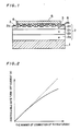
- Fig. 1 is a sectional view showing such a conventional semiconductor device.
- a P-type emitter layer 2a, an N-type base layer 2b and a P-type base layer 2c are formed in this order on the surface of an anode electrode 1, and a plurality of N-type emitter regions 2d are formed on an upper layer part of the P-type base layer 2c at regular intervals.
- a plurality of thyristors 2 are formed by the P-type emitter layer 2a, the N-type base layer 2b, the P-type base layer 2c and the N-type emitter regions 2d.
- Gate electrodes 3 are formed on the surface of the P-type base layer 2c, while cathode electrodes 4 are formed on the respective N-type emitter regions 2d.
- a contact electrode plate 5 is pressed on the cathode electrodes 4 to be electrically in contact therewith in order to electrically connect the cathode electrodes 4 with each other.
- a gate lead wire 6 is electrically connected to the gate electrode 3.
- a gate turn-off thyristor (hereinafter referred to as "GTO") is formed by several hundreds to several thousands of such thyristors 2, each having capacity of several amperes, which are connected in parallel with each other.
- the switching characteristic of the GTO formed in the aforementioned manner depends on the switching performance of each thyristor 2 and the balance performance among the switching characteristics of the respective thyristors 2.
- thyristors 2 of excellent switching performance must be connected in parallel with each other, with no dispersion in characteristic.
- a GTO has such a structure that a current concentration is easily caused at turn-off. Therefore, it is desired to reduce the current concentration of each respective thyristor 2 and to balance the switching characteristics of the thyristors 2 by uniformalizing the current distribution among the thyristors 2 which are connected in parallel with each other.
- a conventional GTO is formed by merely connecting the thyristors 2 in parallel with each other as described above, and no means are provided to reduce the current concentration of each respective thyristor 2 and to make the current distribution among the thyristors 2 uniform.
- the controllable gate turn-off current ( A ) representing the turn-off performance of the GTO is proportional to the number ( n ) of connections of the thyristors 2, as shown by a broken line in Fig. 2.
- controllable gate turn-off current ( A ) is lower when compared with the theoretical value (broken line in Fig. 2) with an increasing number ( n ) of connections of the thyristors 2 as shown by a solid line in Fig. 2, since the thyristors 2 are not balanced in their switching characteristics.
- a GTO of high controllable gate turn-off current cannot be obtained even if the number of connections ( n ) of the thyristors 2 is increased.
- the main object of the present invention is to provide a semiconductor device which has an excellent switching characteristics as well as a high controllable gate turn-off current.
- a semiconductor device comprises a semiconductor element assembly having a plurality of semiconductor elements connected in parallel, a plurality of first electrodes arranged on one surface side of the semiconductor element assembly to be connected with the plurality of semiconductor elements, respectively, a resistor plate which is so arranged that its one surface faces the surfaces of the first electrodes, a conductor plate which is so arranged that its one surface faces the other surface of the resistor plate, and pressure connection means for applying pressure to the other surfaces of the semiconductor element assembly and the conductor plate to create junction surfaces between the first electrodes and the resistor plate as well as between the resistor plate and the conductor plate to connect them with pressure.
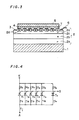
- Fig. 3 is a sectional view showing a semiconductor device according to the present invention.
- a P-type emitter layer 2a, an N-type base layer 2b and a P-type base layer 2c are formed in this order on the surface of an anode electrode 1, and a plurality of N-type emitter regions 2d are formed on an upper layer part of the P-type base layer 2c at regular intervals.
- a plurality of thyristors 2 are formed by the P-type emitter layer 2a, the N-type base layer 2b, the P-type base layer 2c and the N-type emitter regions 2d.
- Gate electrodes 3 are formed on the surface of the P-type base layer 2c. The gate electrodes 3 are electrically connected with each other, although such a connection is not shown in Fig. 3.
- Cathode electrodes 4 are formed on the respective N-type emitter regions 2d.
- a thin resistor plate 7 of uniform thickness is arranged on the cathode electrodes 4, and a contact electrode plate 5 is arranged on the thin resistor plate 7.
- Pressure is applied to the contact electrode plate 5 and the anode electrode 1 by a well-known technique such as an insulated case, whereby the thin resistor plate 7 is pressed on and against the cathode electrodes 4 to be electrically in contact therewith in order to electrically connect all the cathode electrodes 4 with each other. Further, the contact electrode plate 5 is pressed against the thin resistor plate 7 to be electrically in contact therewith.
- Fig. 4 is a circuit diagram showing an equivalent circuit of the semiconductor device shown in Fig. 3.
- thyristors T1 to Tn are respectively connected in series with resistors R1 to Rn, and all these series circuits are connected in parallel with each other.
- the respective resistors R1 to Rn have resistance components of regions corresponding to the respective thyristors T1 to Tn within the thin resistor plate 7, and the respective resistors R1 to Rn are at the same value since the thin resistor plate 7 has a uniform thickness.
- Symbols K , A and G denote a cathode terminal, an anode terminal and a gate terminal, respectively.
- any current concentration is caused in the thyristor T1
- a distributed or partial current i1 is increased as compared with the other partial currents i2 to in.
- I i1 + i2 + i3 + ... + in (1).
- the voltage drop ⁇ VR1 is increased as compared with the voltage drop ⁇ VR2 to ⁇ VRn
- the voltage drop ⁇ VT1 is decreased as compared with the voltage drop ⁇ VT2 to ⁇ VTn as equation (2) is satisfied, and a current across the thyristor T1 is decreased, accordingly.
- the resistor R1 suppresses the current i1 to balance the currents i1 to in, while current re-distribution is performed with respect to the currents i2 to in.
- the resistors R1 to Rn so uniformalize the distributed or partial currents i1 to in as to prevent any local current concentration. Therefore, the respective thyristors 2 can be balanced in switching characteristic, to thereby improve the switching characteristic of the GTO.
- the controllable gate turn-off current ( A ) approaches the theoretical value (broken line in Fig. 2), whereby a GTO of high gate turn-off capacity can be obtained by increasing the number ( n ) of connections of the thyristor 2.
- the present invention is also applicable to a reverse-conductivity type gate turn-off thyristor having a shorted emitter at its anode side, a reverse-blocking type or a reverse-conductivity type gate turn-off thyristor having an NPNP structure or another multi-emitter semiconductor device employing a pressure-contact structure such as a high-power transistor or a high-power electrostatic induction thyristor, to attain a similar effect of improving the switching characteristic of such a semiconductor device.
Landscapes
- Thyristors (AREA)
- Die Bonding (AREA)
Applications Claiming Priority (2)
| Application Number | Priority Date | Filing Date | Title |
|---|---|---|---|
| JP63138006A JPH01307235A (ja) | 1988-06-03 | 1988-06-03 | 半導体装置 |
| JP138006/88 | 1988-06-03 |
Publications (2)
| Publication Number | Publication Date |
|---|---|
| EP0347613A2 true EP0347613A2 (fr) | 1989-12-27 |
| EP0347613A3 EP0347613A3 (fr) | 1990-12-12 |
Family
ID=15211858
Family Applications (1)
| Application Number | Title | Priority Date | Filing Date |
|---|---|---|---|
| EP19890109662 Ceased EP0347613A3 (fr) | 1988-06-03 | 1989-05-29 | Dispositif semi-conducteur comprenant des moyens de contact par pression |
Country Status (2)
| Country | Link |
|---|---|
| EP (1) | EP0347613A3 (fr) |
| JP (1) | JPH01307235A (fr) |
Cited By (1)
| Publication number | Priority date | Publication date | Assignee | Title |
|---|---|---|---|---|
| EP0499707A1 (fr) * | 1991-02-22 | 1992-08-26 | Asea Brown Boveri Ag | Composant semi-conducteur de puissance à commande d'extinction |
Family Cites Families (5)
| Publication number | Priority date | Publication date | Assignee | Title |
|---|---|---|---|---|
| US4127863A (en) * | 1975-10-01 | 1978-11-28 | Tokyo Shibaura Electric Co., Ltd. | Gate turn-off type thyristor with separate semiconductor resistive wafer providing emitter ballast |
| US4327370A (en) * | 1979-06-28 | 1982-04-27 | Rca Corporation | Resilient contact ring for providing a low impedance connection to the base region of a semiconductor device |
| JPS57170566A (en) * | 1981-04-15 | 1982-10-20 | Toshiba Corp | Semiconductor device |
| DE3616233A1 (de) * | 1986-05-14 | 1987-11-19 | Semikron Elektronik Gmbh | Halbleiterbauelement |
| CH670334A5 (fr) * | 1986-09-16 | 1989-05-31 | Bbc Brown Boveri & Cie |
-
1988
- 1988-06-03 JP JP63138006A patent/JPH01307235A/ja active Pending
-
1989
- 1989-05-29 EP EP19890109662 patent/EP0347613A3/fr not_active Ceased
Cited By (2)
| Publication number | Priority date | Publication date | Assignee | Title |
|---|---|---|---|---|
| EP0499707A1 (fr) * | 1991-02-22 | 1992-08-26 | Asea Brown Boveri Ag | Composant semi-conducteur de puissance à commande d'extinction |
| US5221851A (en) * | 1991-02-22 | 1993-06-22 | Asea Brown Boveri Ltd. | Controlled-turn-off high-power semiconductor component |
Also Published As
| Publication number | Publication date |
|---|---|
| JPH01307235A (ja) | 1989-12-12 |
| EP0347613A3 (fr) | 1990-12-12 |
Similar Documents
| Publication | Publication Date | Title |
|---|---|---|
| US3634929A (en) | Method of manufacturing semiconductor integrated circuits | |
| US2721965A (en) | Power transistor | |
| US11056484B2 (en) | Semiconductor device with multiple trench structures | |
| US5089864A (en) | Insulated gate type semiconductor device | |
| US2971139A (en) | Semiconductor switching device | |
| US4161740A (en) | High frequency power transistor having reduced interconnection inductance and thermal resistance | |
| US3525910A (en) | Contact system for intricate geometry devices | |
| US3443171A (en) | Symmetrical switching controlled rectifier with non-overlapped emitters | |
| EP0111166A1 (fr) | Thyristor à blocage par la gâchette | |
| US3896476A (en) | Semiconductor switching device | |
| US4243999A (en) | Gate turn-off thyristor | |
| US4356503A (en) | Latching transistor | |
| EP0064231B1 (fr) | Dispositif semiconducteur à compression | |
| US5021855A (en) | Gate turn-off thyristor | |
| US3622845A (en) | Scr with amplified emitter gate | |
| US3681667A (en) | Controlled rectifier and triac with laterally off-set gate and auxiliary segments for accelerated turn on | |
| US3474303A (en) | Semiconductor element having separated cathode zones | |
| US4862239A (en) | Power semiconductor component | |
| US5365086A (en) | Thyristors having a common cathode | |
| US3755722A (en) | Resistor isolation for double mesa transistors | |
| US4652902A (en) | Power semiconductor device | |
| JPH049378B2 (fr) | ||
| EP0347613A2 (fr) | Dispositif semi-conducteur comprenant des moyens de contact par pression | |
| US4581626A (en) | Thyristor cathode and transistor emitter structures with insulator islands | |
| US3409811A (en) | Four-zone semiconductor rectifier with spaced regions in one outer zone |
Legal Events
| Date | Code | Title | Description |
|---|---|---|---|
| PUAI | Public reference made under article 153(3) epc to a published international application that has entered the european phase |
Free format text: ORIGINAL CODE: 0009012 |
|
| AK | Designated contracting states |
Kind code of ref document: A2 Designated state(s): CH DE GB LI |
|
| PUAL | Search report despatched |
Free format text: ORIGINAL CODE: 0009013 |
|
| AK | Designated contracting states |
Kind code of ref document: A3 Designated state(s): CH DE GB LI |
|
| 17P | Request for examination filed |
Effective date: 19901212 |
|
| 17Q | First examination report despatched |
Effective date: 19920831 |
|
| STAA | Information on the status of an ep patent application or granted ep patent |
Free format text: STATUS: THE APPLICATION HAS BEEN REFUSED |
|
| 18R | Application refused |
Effective date: 19940106 |