EP0346003A2 - Multiprocessor control system - Google Patents
Multiprocessor control system Download PDFInfo
- Publication number
- EP0346003A2 EP0346003A2 EP89305523A EP89305523A EP0346003A2 EP 0346003 A2 EP0346003 A2 EP 0346003A2 EP 89305523 A EP89305523 A EP 89305523A EP 89305523 A EP89305523 A EP 89305523A EP 0346003 A2 EP0346003 A2 EP 0346003A2
- Authority
- EP
- European Patent Office
- Prior art keywords
- switching
- register
- supplied
- vector
- group
- Prior art date
- Legal status (The legal status is an assumption and is not a legal conclusion. Google has not performed a legal analysis and makes no representation as to the accuracy of the status listed.)
- Granted
Links
Images


Classifications
-
- G—PHYSICS
- G06—COMPUTING OR CALCULATING; COUNTING
- G06F—ELECTRIC DIGITAL DATA PROCESSING
- G06F15/00—Digital computers in general; Data processing equipment in general
- G06F15/76—Architectures of general purpose stored program computers
- G06F15/80—Architectures of general purpose stored program computers comprising an array of processing units with common control, e.g. single instruction multiple data processors
- G06F15/8053—Vector processors
- G06F15/8076—Details on data register access
- G06F15/8084—Special arrangements thereof, e.g. mask or switch
-
- G—PHYSICS
- G06—COMPUTING OR CALCULATING; COUNTING
- G06F—ELECTRIC DIGITAL DATA PROCESSING
- G06F9/00—Arrangements for program control, e.g. control units
- G06F9/06—Arrangements for program control, e.g. control units using stored programs, i.e. using an internal store of processing equipment to receive or retain programs
- G06F9/30—Arrangements for executing machine instructions, e.g. instruction decode
- G06F9/38—Concurrent instruction execution, e.g. pipeline or look ahead
- G06F9/3836—Instruction issuing, e.g. dynamic instruction scheduling or out of order instruction execution
- G06F9/3851—Instruction issuing, e.g. dynamic instruction scheduling or out of order instruction execution from multiple instruction streams, e.g. multistreaming
Definitions
- the present invention generally relates to a multiprocessor system, and particularly to a multiprocessor system having a plurality of scalar units and a single vector unit, which selectively executes vector instructions supplied from the scalar units. More particularly, the present invention relates to a control system which selects vector instructions from the scalar units to be executed in the vector unit.
- a multiprocessor system having a plurality of scalar units each processing a scalar instruction, and a single vector unit which processes a vector instruction at high speeds.
- a vector instruction is executed in such a way that the right to use the vector unit is selectively assigned the plurality of scalar units.
- the vector unit since the vector unit includes pipelines each consisting of a plurality of processing stages, it takes long to start executing a vector instruction after the vector instruction is selected.
- a multiprocessor system records how long the vector unit is exclusively used for each scalar unit, on the basis of a timing with which the scalar unit being selected is switched to another scalar unit. The recorded time is based on accounting.
- a more specific object of the present invention is to provide a multiprocessor control system capable of satisfying a variety of needs by selectively setting a timing with which the right to use a vector unit is switched among scalar units.
- a multiprocessor control system adapted to a multiprocessor system including a plurality of first execution units each processing a first group of instructions, and a single second execution unit processing a second group of instructions supplied from the plurality of first execution units, the second execution unit including a plurality of pipelines used for executing the second group of instructions, the multiprocessor control system comprising the following circuit.
- a switching circuit selectively switches the second group of instructions supplied from the first execution units to thereby select the second group of instructions relating to one of the plurality of first execution units.
- a control stage circuit includes a plurality of register stages used for controlling a pipeline process.
- the control stage circuit sequentially stores the second group of instructions relating to the selected one of the first execution units in the register stages and outputs, for every register stage, a state indicating signal indicating state information on the corresponding register stage.
- a switching mode setting circuit generates a mode setting signal used for selecting one of a plurality of switching modes each defining a timing with which the switching by the switching circuit is done.
- a switching control circuit generates the switching signal based on the state indicating signals output from the control stage circuit and the mode setting signal indicative of one of the plurality of switching modes supplied from the switching mode setting circuit.
- the switching mode setting circuit is controlled so as to select one of the switching modes which defines a timing enabling it possible to record an accurate of each of the first execution units for accounting, for example.
- the switching mode setting circuit is controlled so as to select another one of the switching modes which defines another timing making it possible to execute the second group of instructions at high speeds. It is preferable that a user freely accesses the switching mode setting circuit and selects desired one of the switching modes.
- FIG.1 A description is now given of the overall structure of a multiprocessor system with reference to FIG.1.
- the illustrated block diagram itself is described in Japanese Laid-Open Patent Application Nos. 62-9460 and 214467. It is noted that the present invention relates to an improvement of a vector control unit as will be described in detail later.
- a multiprocessor system includes two scalar units (SU0, SU1) 12 and 13, and a single vector unit (VU) 14.
- the scalar units 12 and 13 are connected to a memory control unit (MCU) 1b, which controls a main memory unit (MSU) 1a.
- the vector unit 14 includes a vector execute unit (VEU) 15 and a vector control unit (VCU) 16.
- the vector control unit 16 is connected to the scalar units 12 and 13, and the vector execute unit 15 is connected to the memory control unit 1b, and the vector control unit 16.
- the vector execution unit 15 is made up of a load pipeline 150, a store pipeline 151, a vector register (VR) 152, an addition pipeline 153, a multiplication pipeline 154, and a division pipeline 155.
- the vector control unit 16 has the function of controlling vector instructions in a unit of instruction vector.
- the vector control unit 16 enters one or more vector instructions related to selected one of the scalar units 12 and 13.
- the vector control unit 16 generates supervisory information related to the pipelines 150 through 155.
- the generated supervisory information is transferred to the vector execute unit 15 through a signal line 160.
- the load pipeline 150 and the store pipeline 151 of the vector execute unit 15 are used for data transfer between the vector register 152 and the main memory unit 1a.
- the addition, multiplication and division pipelines 153, 154 and 155 are used for carrying out a vector operation on vector data (operand) read out of the vector register 152, and writing resultant vector data into the vector register 152.
- a fetch of an instruction from the main memory unit 1a is carried out by the scalar units 12 and 13.
- each of the scalar units 12 and 13 fetches a scalar instruction, it executes the related scalar instruction therein.
- each of the scalar units 12 and 13 fetches a vector instruction, it passes the vector instruction to the vector control unit 16.
- the vector unit 14 selects vector instructions supplied from the scalar units 12 and 13, and executes the same.
- the vector execute unit 15 has processed a packet consisting of a plurality of consecutive vector instructions supplied from either the scalar unit 12 or 13, the vector control unit 16 can select vector instructions supplied from the other scalar unit and execute the same.
- Each of the scalar units 12 and 13 includes a timer called a CPU timer used for recording a time it takes to execute an instruction (a CPU operating time).
- the CPU timer of each of the scalar units 12 and 13 is controlled as will be described later.
- vector instructions related to the other scalar unit are inhibited from being executed in the vector unit 14, and therefore the CPU timer in the related scalar unit is set inactive.
- FIGS.2A and 2B illustrate the relations between the switching between the scalar units 12 and 13 and respective CPU operating times.
- the CPU timer of the scalar unit 12 (system #0) records the CPU operating time during the time when the vector unit 14 is coupled to the scalar unit 12.
- the scalar unit 13 (system #1) becomes coupled to the vector unit 14 in place of the scalar unit 12.
- the CPU timer of the scalar unit 12 stops recording the CPU operating time, and on the other hand, the CPU timer of the scalar unit 13 starts recording. In this case, it is possible to obtain an accurate CPU operating time; however an overhead occurring at the time of switching is large, and therefore, the above process is wasteful of time intervals t1 and t2.
- the scalar units 12 and 13 are selectively connected to the vector unit 14, before the vector unit 14 has processed all the vector instructions (in the illustrated case, the vector unit starts processing the vector instructions supplied from the scalar unit 13 when the execution of the last vector instruction related to the scalar unit 12 is started).
- the overhead time can extremely be reduced.
- the present invention makes it possible to selectively provide a timing with which the scalar unit to be connected to the vector unit 14 is switched.
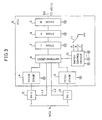
- the vector control unit 16 includes fetch stages 4 and 5 (related to the scalar units 12 and 13, respectively), a switching circuit 6, three stages 7, 8 and 9 provided for the pipeline process of vector instructions, a switching control circuit 10, and a mode setting switch 11.
- the mode setting switch 11 is used for selecting one of a plurality of switching modes (three modes A, B and C are provided in the illustrated structure).
- the switching control circuit 10 is informed of the selected mode by a switching mode signal supplied from the mode setting switch 11.
- the switching control circuit 10 is supplied with state indicating signals a through e, which are output from the fetch stages 4, 5, and the first, second and third stages 7, 8, 9, respectively.
- state indicating signals a through e become indicative of the switching mode designated by the mode setting switch 11
- the switching control circuit 10 supplies a related switch signal to the switching circuit 6.
- each of the state indicating signal represents presence/absence of a vector instruction therein.
- each state indicating signal indicates the scalar unit to which the stored vector instruction is related.
- the mode setting switch selects one of the switching modes A, B and C.
- Examples of the switching modes A, B and C are as follows.
- the switching mode A is a mode in which the switching is performed when all vector instructions related to one of the scalar units 12 and 13 completely go out of all the stages 4, 5, 7, 8 and 9.
- the switching mode B is a mode in which the switching is performed when vector instructions related to one of the scalar units 12 and 13 completely go out of the third stage 9.
- the mode C is a mode in which the switching is performed when vector instructions related to one of the scalar units 12 and 13 completely go out of the second stage 8.
- the switching control circuit 10 outputs the switch signal when the selected state is detected.
- the right to use the vector unit 14 is given the selected one of the scalar units 12 and 13.
- the CPU timer of the selected scalar unit is started supplied from a timer control signal, which is derived from the switching circuit 6 and is supplied to the scalar units 12 and 13 through signal lines L1 and L2.
- the number of stages to be cascaded is not limited to 3.
- the mode A is selected by the mode setting switch 11.
- the mode B or C is selected by the mode setting switch 11.
- FIG.4 there is illustrated a configuration of the structure of the vector control unit 16 constructed according to the embodiment of the present invention.
- the scalar units 12 and 13 are connected to vector fetch stages 23 and 24 (VFS0, VFS1) through buses BUS1 and BUS2, respectively.
- the vector fetch stage 23 includes a vector fetch stage register (VFSR0) 23-1, a vector fetch buffer (VFB0) 23-2, and a selector (SEL) 23-3.
- the vector fetch stage 23 includes a logic circuit, which will be described in detail later.
- the vector fetch stage (VFS1) 24 includes a vector fetch register (VFSR1)) 24-1, a vector fetch buffer (VFB1) 24-2, a selector (SEL) 24-3, and a logic circuit (not shown).
- the vector fetch stages 23 and 24 correspond to the fetch stages 4 and 5 shown in FIG.3, respectively.
- the selectors 23-3 and 24-3 are connected to a switching circuit 25, which corresponds to the switching circuit 6 illustrated in FIG.3.
- the switching circuit 25 is followed by a vector pre-decode stage (VPS) 28, which indicates one of the scalar units 12 and 13 to which a vector instruction existing therein is related.
- the state indicating signal related to the vector pre-decode stage 28 is generated therein and supplied to a switching control circuit 26.
- the vector pre-decode stage 28 and the switching control circuit 26 correspond to the first stage 7 and the switching control circuit 10 shown in FIG.3, respectively.
- the switching control circuit 26 is supplied with busy signals derived from the aforementioned logic circuits provided in the vector fetch stages 23 and 24. The busy signals will be described in detail later.
- the vector pre-decode stage 28 precedes to a vector queue stage (VQS) 29, which temporarily stores vector instructions supplied from the vector pre-decode stage 28.
- VQS vector queue stage
- the state indicating signal related to the vector queue stage 29 is generated therein and supplied to the switching control circuit 26.
- the vector queue stage 29 corresponds to the second stage 8 shown in FIG.3.
- a vector execute stage (VES) 30 follows the vector queue stage 30, and includes a supervisory register related to each of the pipelines 150, 151, 153, 154 and 155 shown in FIG.1.
- the supervisory registers store data which controls the start and end of the execution of the vector instructions to be executed in the corresponding pipelines 150, 151, 153, 154 and 155.
- the stage indicating signal related to the vector execute stage 30 is generated therein and supplied to the switching control circuit 26.
- the vector execute stage 30 corresponds to the third stage 9 shown in FIG.3.
- a mode setting circuit 27 is connected to the switching control circuit 26, and selects one of the three switching modes by closing the corresponding contact.
- the mode setting circuit 27 corresponds to the mode setting circuit 10 shown in FIG.3.
- vector instructions from the scalar units 12 and 13 are supplied to the vector fetch registers 23-1 and 24-1 through the buses BUS1 and BUS2, respectively.
- system #0 an operation related to the scalar unit 12
- the following operation is carried out.
- the fetched vector instruction is supplied from the vector fetch register 23-1 to the vector pre-decode stage 28 through the selector 23-3 and the switching circuit 25.
- the fetched vector instruction relating to the scalar unit 12 is transferred from the vector fetch register 23-1 to the vector fetch buffer 23-2, and is stored therein.
- a vector instruction which is placed at top of the vector instructions stored in the vector fetch buffer 23-2, is read out of the vector fetch buffer 23-2, when the switching circuit 25 selects the scalar unit 12.
- the switching control circuit 26 selectively determines which one of the vector instructions sent from the scalar units 12 and 13 should be selected and supplied to the vector pre-decode stage 28.
- This switching control means the switching of the right to use the vector unit 14 in a unit of instruction packet.
- An instruction packet is defined as a sequence of consecutive vector instructions which can successively be executed with no interruption thereof. Therefore, for example, the switching circuit 25 operates in such a manner that an instruction packet relating to the scalar unit 12 is completely executed, and thereafter the execution of an instruction packet relating to the scalar unit 13 is started.
- the right to use the vector unit 14 is exclusively switchable between the scalar units 12 and 13.
- vector instructions related to one of the scalar units 12 and 13 which has obtained the right are set the vector pre-decode stage 28 at the next operating stage.
- the vector instruction selected by the selector 25 in accordance with the switch signal supplied form the switching control circuit 26, is decoded by the vector pre-decode stage 28. Thereby, it can be found that which one of the scalar units 12 and 13 the received vector instruction relates to. Then, the vector instruction in the vector pre-decode stage 28 is stored in the vector queue stage 29. Thereafter, the vector instruction read out of the vector queue stage 29 is supplied to the vector execute stage 30, which manages the access to the main memory unit 1a (FIG.1) and operation. At the same time as the vector execute stage 30 receives the vector instruction, it sends supervisory information to one of the pipelines 150, 151, 153, 154 and 155 to be executed. Thereafter, when the execution of the vector instruction is completed, the used pipeline is released from the execution.
- the switching control circuit 26 is supplied with the switching mode signal indicative of one of the switching modes M1, M2 and M3 selected by the mode setting switch 27.
- the switching control circuit 26 includes a first busy detecting circuit 26-1 shown in FIG.5A relating to the scalar unit 12 (system #0), and a second busy detecting circuit 26-2 shown in FIG.5B relating to the scalar unit 13 (system #1).
- An output signal of each of the first and second busy detecting circuits 26-1 and 26-2 is supplied to the switching circuit 25, a detailed configuration of which is illustrated in FIG.6.
- a busy signal VFS0-BUSY0 generated by the vector fetch register 23-1 is supplied to OR gates 31, 32 and 33.
- the busy signal VFS0-BUSY0 indicates whether or not a vector instruction relating to system #0 exists in the vector fetch stage 23.
- a busy signal VPS-BUSY0 generated by the vector pre-decode stage 28 is supplied to the OR gates 31, 32 and 33.
- the busy signal VPS-BUSY0 indicates whether or not a vector instruction relating to system #0 exists in the vector pre-decode stage 28.
- a busy signal VQS-BUSY0 generated by the vector queue stage 29 is supplied to the OR gates 31 and 32.
- the busy signal VQS-BUSY0 indicates whether or not a vector instruction relating to system #0 exists in the vector queue stage 29.
- a busy signal VES-BUSY0 generated by the vector execute stage 30 is supplied to the OR gate 31.
- the busy signal VES-BUSY0 indicates whether or not a vector instruction relating to system #0 exists in the vector execute stage 30.
- Output terminals of the OR gates 31, 32 and 33 are connected to input terminals of AND gates 34, 35 and 36, respectively.
- the switching mode signals M1, M2 and M3 derived from the mode setting circuit 27 are supplied to the AND gates 34, 35 and 36, respectively.
- Output terminals of the AND gates 34, 35 and 36 are connected to input terminals of an OR gate 37, which outputs a busy signal BUSY0.
- Each of the above-mentioned busy signals VFS0-BUSY0, VPS-BUSY0, VQS-BUSY0 and VES-BUSY0 is "1" when a vector instruction exists in the related stage, and is "0" when no vector instruction exists in the related stage.
- the OR gate 31 outputs "1” when a vector instruction exists in at least one of the four stages 23, 28, 29 and 30.
- the OR gate 32 outputs "1" when a vector instruction exists in at least one of the three stages 23, 28 and 29.
- the OR gate 33 outputs "1" when a vector instruction exists in at least one of the two stages 23 and 28.
- the AND gate 34 performs an AND operation on the output signal of the OR gate 31 and the switching mode signal M1.
- the AND gate 35 performs an AND operation on the output signal of the OR gate 32 and the switching mode signal M2.
- the AND gate 36 performs an AND operation on the output signal of the OR gate 33 and the switching mode signal M3.
- the aforementioned busy signal BUSY0 is generated by performing an OR operation on the output signals of the AND gates 34, 35 and 36 in the OR gate 37.
- the busy signal BUSY0 When the busy signal BUSY0 is "1", the busy signal BUSY0 represents that it is impossible to perform the switching based on the designated switching mode, or in other words, there are vector instructions relating to system #0 in the designated stages. On the other hand, when the busy signal BUSY0 is switched to "0", this change of the busy signal BUSY0 represents that all vector instructions relating to system #0 have gone out of the designated stages and therefore the switching from system #0 to system #1 becomes available.
- a busy signal VFS1-BUSY1 generated by the vector fetch register 23-1 is supplied to OR gates 41, 42 and 43.
- the busy signal VFS1-BUSY1 indicates whether or not a vector instruction relating to system #1 exists in the vector fetch stage 24.
- a busy signal VPS-BUSY1 generated by the vector pre-decode stage 28 is supplied to the OR gates 41, 42 and 43.
- the busy signal VPS-BUSY1 indicates whether or not a vector instruction relating to system #1 exists in the vector pre-decode stage 28.
- a busy signal VQS-BUSY1 generated by the vector queue stage 29 is supplied to the OR gates 41 and 42.
- the busy signal VQS-BUSY1 indicates whether or not a vector instruction relating to system #1 exists in the vector queue stage 29.
- a busy signal VES-BUSY1 generated by the vector execute stage 30 is supplied to the OR gate 41.
- the busy signal VES-BUSY1 indicates whether or not a vector instruction relating to system #1 exists in the vector execute stage 30.
- Output terminals of the OR gates 41, 42 and 43 are connected to input terminals of AND gates 44, 45 and 46, respectively.
- the switching mode signals M1, M2 and M3 derived from the mode setting circuit 27 are supplied to the AND gates 44, 45 and 46, respectively.
- Output terminals of the AND gates 44, 45 and 46 are connected to input terminals of an OR gate 47, which outputs a busy signal BUSY 1.
- Each of the above-mentioned busy signals VFS1-BUSY1, VPS-BUSY1, VQS-BUSY1 and VES-BUSY1 is "1" when a vector instruction exists in the related stage, and is "0" when no vector instruction exists in the related stage.
- the OR gate 41 outputs "1” when a vector instruction exists in at least one of the four stages 23, 28, 29 and 30.
- the OR gate 42 outputs "1" when a vector instruction exists in at least one of the three stages 23, 28 and 29.
- the OR gate 43 outputs "1" when a vector instruction exists in at least one of the two stages 23 and 28.
- the AND gate 44 performs an AND operation on the output signal of the OR gate 41 and the switching mode signal M1.
- the AND gate 45 performs an AND operation on the output signal of the OR gate 42 and the switching mode signal M2.
- the AND gate 46 performs an AND operation on the output signal of the OR gate 43 and the switching mode signal M3.
- the aforementioned busy signal BUSY1 is generated by performing an OR operation on the output signals of the AND gates 44, 45 and 46 in the OR gate 47.
- the busy signal BUSY1 When the busy signal BUSY1 is "1", the busy signal BUSY1 represents that it is impossible to perform the switching based on the designated switching mode, or in other words, there are vector instructions relating to system #1 in the designated stages. On the other hand, when the busy signal BUSY1 is switched to "0", this change of the busy signal BUSY1 represents that all vector instructions relating to system #1 have gone out of the designated stages, and therefore the switching from system #1 to system #0 becomes available.
- FIG.6 illustrates an example of the structure for the switching circuit 25.
- the switching circuit 25 includes a set-reset type latch circuit (SR0) 50 in which a set operation has priority over a reset operation, a set-reset type latch circuit (SR1) 51 in which a reset operation has priority over a set operation, AND gates 52, 53, an OR gate 54, and inverters 55, 56, 57 and 58.
- SR0 set-reset type latch circuit
- SR1 set-reset type latch circuit
- the output signal of the latch circuit 50 passes through the inverter 57 and is then supplied to the scalar unit 12.
- the output signal of the inverter 57 is "1" when the scalar unit 12 is not selected. At this time, the CPU timer of the scalar unit 12 is stopped.
- the output signal of the latch circuit 51 passes through an inverter 58 and is then supplied to the scalar unit 13.
- the output signal of the inverter 58 is "1" when the scalar unit 13 is not selected. At this time, the CPU timer of the scalar unit 13 is stopped.
- the switching mode M1 shown in FIG.7(A) when the last vector instruction of the instruction packet relating to system #0 is completed (or goes out of the vector execute stage 30), the right to use the vector unit 14 assigned the scalar unit 12 is turned OFF to thereby stop the time recording by the CPU timer of the scalar unit 12, and on the other hand, the right of the use of the vector unit 14 is turned ON (assigned the scalar unit 13) to thereby start the time recording by the CPU timer of the scalar unit 13. With this timing, a vector instruction is set in the vector pre-decode lo stage 28, and immediately set in the vector queue stage 29. In the switching mode M1, there is no overlap of CPU operating time between the systems #0 and #1. It follows that there occurs no error in the recording of the CPU operating times. However, the switching mode M1 is wasteful of time intervals DT1 shown in FIG.7(A).
- a vector instruction relating to system #1 (top vector instruction) is to be next executed, is being used for executing a vector instruction relating to system #0, the above vector instruction relating to system #1 waits in the vector queue stage 29 until the above pipeline is released from the use exclusive to system #0. In other cases, the vector instruction relating to system #1 is immediately sent to the designated one of the pipelines.
- Operation occurring at the time of switching from system #1 to system #0 is similar to that for the switching from system #0 to system #1.
- the vector fetch stage 23 includes a logic circuit 23-4 in addition to the aforementioned vector fetch register (VFSR0) 23-1, vector fetch buffer (VFB0) 23-2, and selector (SEL) 23-3.
- the vector fetch register 23-1 includes a flag register VFSR0-VALID.
- the vector fetch buffer 23-2 includes buffer portions VFB00 and VFB01. When a vector instruction is being registered in the buffer portion VFB00, "1" is set in an associated flag register VFB00-VALID. For the same purpose, a flag register VFB01-VALID is provided with respect to the buffer portion VFB00.
- the selector 23-3 includes AND gates 23a, 23b, and an OR gate 23c.
- the AND gates 23a and 23b are connected to the vector fetch register 23-1 and the vector fetch buffer 23-2, respectively. Further, the AND gates 23a and 23b are supplied with select signals SELECT-VFSR0 and SELECT-VFB0, respectively, which are generated by the logic circuit 23-4. Output terminals of the AND gates 23a and 23b are connected to the OR gate 23c, which is connected to the switching circuit 25.
- the logic circuit 23-4 is made up of OR gates 23d, 23e, and an inverter 23f.
- the OR gate 23d is supplied with the state signals stored in the flag registers VFB00-VALID and VFB01-VALID.
- the OR gate 23e is supplied with the state signal stored in the flag register VFSR0-VALID and an output signal of the OR gate 23d.
- the output signal of the OR gate 23d is the select signal SELECT-VFB0 to be supplied to the AND gate 23b, and is also supplied to the AND gate 23a through the inverter 23f, as the select signal SELECT-VFSR0.
- the output signal of the OR gate 23e is the aforementioned busy signal VFS0-BUSY0.
- a vector instruction supplied from the scalar unit 12 is set in the vector fetch register 23-1.
- a valid signal of "1" is set in the flag register VFSR0-VALID associated with the vector fetch register 23-1.
- the select signal SELECT VFSR0 is "1".
- the selector 23-3 selects the vector instruction supplied from the vector fetch register 23-1.
- FIG.9 illustrates an example of the structure for the vector pre-decode stage (VPS) 28.
- the vector pre-decode stage 28 includes a vector pre-decode stage register (VPSR) 28-1, and a logic circuit 28-2 made up of an inverter 28a and AND gates 28b and 28c.
- the vector pre-decode stage register 28-1 includes flag registers VPSR-SU1 and VPSR-VALID.
- VPSR-SU1 flag registers VPSR-SU1
- VPSR-VALID When a vector instruction is supplied to the vector pre-decode stage register 28-1 from the vector fetch stage 23, a value of "1" is written into the flag register VPSR-VALID, and a value of "0" is written into the register VPSR-SU1.
- the state where there are values of "1" and "0" in the flag registers VPSR-VALID and VPSR-SU1, respectively, means that a vector instruction relating to system #0 is set in the vector pre-decode flag register 28-1.
- the logic circuit 28-2 sets the busy signal VPS-BUSY0 to "1".
- the valid signal stored in the flag register VPSR-VALID is supplied to the AND gates 28b and 28c.
- the state signal stored in the flag register VPSR-SU1 is supplied to the AND gate 28b, and the AND gate 28c through the inverter 28a.
- the AND gates 28b and 28c output the busy signals VPS-BUSY0 and VPS-BUSY1, respectively.
- the state where a value of "1" is set in each of the flag registers VPSR-VALID and VPSR-SU1, means that a vector instruction relating to system #1 is set in the vector pre-decode stage register 28-1.
- the busy signal VPS-BUSY1 is set to "1".
- the busy signals VPS-BUSY0 and VPS-BUSY1 are sent to the switching control circuit 26.
- FIG.10 illustrates an example of the structure for the vector queue stage 29.
- the vector queue stage 29 includes a register (AQSR) 29-1, a register (EQSR) 29-2, a selector (SEL) 29-3, and a logic circuit 29-4.
- the register 29-1 includes flag registers AQS-VALID and AQS-SU1
- the register 29-2 includes flag registers EQS-VALID and EQS-SU1.
- he register 29-2 includes flag registers EQS-VALID and EQS-SU1.
- the vector instruction is a vector instruction which uses one of the addition pipeline 153, the multiplication pipeline 154 and the division pipeline 155
- the above vector instruction is written into the register 29-2.
- the valid signal stored in the flag register VPSR-VALID shown in FIG.9 is set in either the flag register AQS-VALID or EQS-VALID.
- the state signal stored in the flag register VPSR-SU1 is set in either the flag register AQS-SU1 or the register EQS-SU1.
- the vector instructions in the registers 29-1 and 29-2 are sequentially read out starting from an executable vector instruction contained therein, and are supplied to the vector execute stage 30.
- the valid signal stored in the flag register AQSR-VALID is supplied to AND gates 29a and 29b of the logic circuit 29-4.
- the state signal stored in the flag register AQS-SU1 is supplied to the AND gate 29b, and the AND gate 29a through an inverter 29e.
- the output signals of the AND gates 29a and 29b are supplied to OR gates 29g and 29h, respectively.
- the valid signal stored in the flag register EQS-VALID is supplied to the AND gates 29c and 29d.
- the state signal stored in the flag register EQS-SU1 is supplied to the AND gate 29d, and the AND gate through an inverter 29f.
- the output signals of the AND gates 29c and 29d are supplied to the OR gates 29g and 29h, respectively.
- the OR gates 29g and 29h output the busy signals VQS-BUSY0 and VQS-BUSY1, respectively, which are supplied to the switching control circuit 26.
- the busy signal VQS-BUSY0 is "1"
- the value of the busy signal VQS-BUSY1 is determined.
- the busy signals VQS-BUSY0 and VQS-BUSY1 generated in this manner are supplied to the switching control circuit 26.
- the vector execute stage 30 has the illustrated supervisory circuit for each of the load pipeline 150, the store pipeline 151, the addition pipeline 153, the multiplication pipeline 154 and the division pipeline 155.
- the following description relates to the structure of the supervisory circuit provided for the load pipeline 150 (a load supervisory circuit).
- the supervisory circuit is made up of a register (LRSR) 30-1, a register (LWSR) 30-2, counters 30-3, 30-4, and a logic circuit 30-5.
- LRSR register
- LWSR register
- a vector instruction supplied from the vector queue stage 29 is set in the register 30-1, which includes flag registers LRSR-VALID and LRSR-SU1.
- the counter 30-3 is set to 0, and starts counting.
- the vector instruction stored in the register 30-1 is supplied to the load pipeline 150 through the signal line 160.
- the counter 30-3 counts a value determined by the received vector instruction (read time)
- the vector instruction is read out of the register 30-1 and is then set in the register 30-2.
- the counter 30-4 is set to "0", and then starts counting.
- the counted value of the counter 30-4 reaches a value indicative of a time it takes to execute the vector instruction of concern (write time)
- the execution of the vector instruction is ended.
- the above circuit is the same as the logic circuit 29-4 shown in FIG.10.
- the busy signal LSR-BUSY0 is "1".
- the busy signal LSR-BUSY1 is "1".
- An OR gate 30i included in the logic circuit 30-5 is supplied to busy signals LSR-BUSY0, SSR-BUSY0, ASR-BUSY0, MSR-BUSY0, and DSR-BUSY0 with respect to the pipelines 150, 151, 153, 154 and 155, respectively. Then the OR gate generates a busy signal VES-BUSY0, which is supplied to the switching control circuit 26. Similarly, an OR gates 30j generates a busy signal VES-BUSY1 from busy signals LSR-BUSY1, SSR-BUSY1, ASR-BUSY1, MSR-BUSY1, and DSR-BUSY1 with respect to the pipelines 150, 151, 153, 154 and 155, respectively. The busy signals VES-BUSY0 and VES-BUSY1 thus generated are supplied to the switching control circuit 26.
- the present invention is not limited to the above-mentioned embodiment.
- an arbitrary number of stages provided in the vector control unit 16 may be used.
- the busy signal generated at each stage may be generated based only on whether one of the scalar units 12 and 13 is related to the stored vector instruction. This is because the scalar units 12 and 13 are alternately selected.
- the above-mentioned embodiment relates to a multiprocessor system having a plurality of scalar units and a single vector unit.
- the present invention includes a multiprocessor system which includes a plurality of small-scale execution units and a single large-scale execution unit.
Landscapes
- Engineering & Computer Science (AREA)
- Theoretical Computer Science (AREA)
- Software Systems (AREA)
- Physics & Mathematics (AREA)
- General Engineering & Computer Science (AREA)
- General Physics & Mathematics (AREA)
- Computer Hardware Design (AREA)
- Multimedia (AREA)
- Computing Systems (AREA)
- Advance Control (AREA)
- Complex Calculations (AREA)
- Multi Processors (AREA)
Abstract
Description
- The present invention generally relates to a multiprocessor system, and particularly to a multiprocessor system having a plurality of scalar units and a single vector unit, which selectively executes vector instructions supplied from the scalar units. More particularly, the present invention relates to a control system which selects vector instructions from the scalar units to be executed in the vector unit.
- Conventionally, there is known, as a computer for technological computation, a multiprocessor system having a plurality of scalar units each processing a scalar instruction, and a single vector unit which processes a vector instruction at high speeds. In such a multiprocessor system, a vector instruction is executed in such a way that the right to use the vector unit is selectively assigned the plurality of scalar units. Conventionally, since the vector unit includes pipelines each consisting of a plurality of processing stages, it takes long to start executing a vector instruction after the vector instruction is selected.
- Therefore, it is desired to switch one scalar unit to another scalar unit, before the execution of a scalar instruction being processed is not completed to thereby enhance the efficiency of processing. However, it is impossible to satisfy a variety of needs for multiprocessor systems by simply selecting one of the scalar units before the execution of a scalar instruction is completed. For example, generally, a multiprocessor system records how long the vector unit is exclusively used for each scalar unit, on the basis of a timing with which the scalar unit being selected is switched to another scalar unit. The recorded time is based on accounting. It would be understood that accounting is no longer performed accurately in the case where the switching of the connection between the vector unit and one of the scalar units is performed before the execution of a scalar instruction being processed is not completed. Further, there is also a need for efficiently carrying out a computation irrespective of operating time.
- It is therefore a general object of the present invention to provide an improved multiprocessor control system in which the above-mentioned disadvantages are eliminated.
- A more specific object of the present invention is to provide a multiprocessor control system capable of satisfying a variety of needs by selectively setting a timing with which the right to use a vector unit is switched among scalar units.
- The above objects of the present invention can be achieved by a multiprocessor control system adapted to a multiprocessor system including a plurality of first execution units each processing a first group of instructions, and a single second execution unit processing a second group of instructions supplied from the plurality of first execution units, the second execution unit including a plurality of pipelines used for executing the second group of instructions, the multiprocessor control system comprising the following circuit. A switching circuit selectively switches the second group of instructions supplied from the first execution units to thereby select the second group of instructions relating to one of the plurality of first execution units. A control stage circuit includes a plurality of register stages used for controlling a pipeline process. The control stage circuit sequentially stores the second group of instructions relating to the selected one of the first execution units in the register stages and outputs, for every register stage, a state indicating signal indicating state information on the corresponding register stage. A switching mode setting circuit generates a mode setting signal used for selecting one of a plurality of switching modes each defining a timing with which the switching by the switching circuit is done. A switching control circuit generates the switching signal based on the state indicating signals output from the control stage circuit and the mode setting signal indicative of one of the plurality of switching modes supplied from the switching mode setting circuit. The switching mode setting circuit is controlled so as to select one of the switching modes which defines a timing enabling it possible to record an accurate of each of the first execution units for accounting, for example. On the other hand, the switching mode setting circuit is controlled so as to select another one of the switching modes which defines another timing making it possible to execute the second group of instructions at high speeds. It is preferable that a user freely accesses the switching mode setting circuit and selects desired one of the switching modes.
- Other objects, features and advantages of the present invention will become apparent from the following detailed description when read in conjunction with the accompanying drawings.
-
- FIG.1 is a block diagram of a multiprocessor system;
- FIGS.2A and 2B are timing charts illustrating a conventional scalar unit switching process;
- FIG.3 is a block diagram of an essential part of the present invention;
- FIG.4 is a block diagram of an essential part of a preferred embodiment of the present invention;
- FIGS.5A and 5B are circuit diagrams illustrating circuits included in a switching control circuit used in the embodiment of FIG.4;
- FIG.6 is a circuit diagram of a switching circuit used in the embodiment;
- FIG.7 is a timing chart illustrating operations of the embodiment;
- FIG.8 is a circuit diagram of an example of the structure of a vector fetch stage used in the embodiment;
- FIG.9 is a circuit diagram of an example of the structure of a vector pre-decode stage used in the embodiment;
- FIG.10 is a circuit diagram of an example of the structure of a vector queue stage used in the embodiment; and
- FIG.11 is a circuit diagram of a part of a vector execute stage used in the embodiment.
- A description is now given of the overall structure of a multiprocessor system with reference to FIG.1. The illustrated block diagram itself is described in Japanese Laid-Open Patent Application Nos. 62-9460 and 214467. It is noted that the present invention relates to an improvement of a vector control unit as will be described in detail later.
- Referring to FIG.1, a multiprocessor system includes two scalar units (SU0, SU1) 12 and 13, and a single vector unit (VU) 14. The
scalar units vector unit 14 includes a vector execute unit (VEU) 15 and a vector control unit (VCU) 16. Thevector control unit 16 is connected to thescalar units vector execute unit 15 is connected to thememory control unit 1b, and thevector control unit 16. Thevector execution unit 15 is made up of aload pipeline 150, astore pipeline 151, a vector register (VR) 152, anaddition pipeline 153, amultiplication pipeline 154, and adivision pipeline 155. - The
vector control unit 16 has the function of controlling vector instructions in a unit of instruction vector. When receiving vector instructions supplied from thescalar units vector control unit 16 enters one or more vector instructions related to selected one of thescalar units vector control unit 16 generates supervisory information related to thepipelines 150 through 155. The generated supervisory information is transferred to thevector execute unit 15 through asignal line 160. Theload pipeline 150 and thestore pipeline 151 of thevector execute unit 15 are used for data transfer between thevector register 152 and themain memory unit 1a. The addition, multiplication anddivision pipelines vector register 152, and writing resultant vector data into thevector register 152. - In operation, a fetch of an instruction from the
main memory unit 1a is carried out by thescalar units scalar units scalar units vector control unit 16. Thevector unit 14 selects vector instructions supplied from thescalar units vector execute unit 15 has processed a packet consisting of a plurality of consecutive vector instructions supplied from either thescalar unit vector control unit 16 can select vector instructions supplied from the other scalar unit and execute the same. - Each of the
scalar units scalar units scalar unit vector unit 14, and therefore the CPU timer in the related scalar unit is set inactive. - FIGS.2A and 2B illustrate the relations between the switching between the
scalar units vector unit 14 is coupled to thescalar unit 12. When the vector instructions related to thescalar unit 12 is completely processed, the scalar unit 13 (system #1) becomes coupled to thevector unit 14 in place of thescalar unit 12. At this time, the CPU timer of thescalar unit 12 stops recording the CPU operating time, and on the other hand, the CPU timer of thescalar unit 13 starts recording. In this case, it is possible to obtain an accurate CPU operating time; however an overhead occurring at the time of switching is large, and therefore, the above process is wasteful of time intervals t₁ and t₂. - On the other hand, as shown in FIG.2B, the
scalar units vector unit 14, before thevector unit 14 has processed all the vector instructions (in the illustrated case, the vector unit starts processing the vector instructions supplied from thescalar unit 13 when the execution of the last vector instruction related to thescalar unit 12 is started). In this case, the overhead time can extremely be reduced. However, it is impossible to record the CPU operating time with precision. - The present invention makes it possible to selectively provide a timing with which the scalar unit to be connected to the
vector unit 14 is switched. - A description is given of a fundamental construction of the present invention with reference to FIG.3. Essential features of the present invention exist in the construction of the
vector control unit 16. Referring to FIG.3, thevector control unit 16 includes fetchstages 4 and 5 (related to thescalar units switching circuit 6, threestages control circuit 10, and a mode setting switch 11. The mode setting switch 11 is used for selecting one of a plurality of switching modes (three modes A, B and C are provided in the illustrated structure). The switchingcontrol circuit 10 is informed of the selected mode by a switching mode signal supplied from the mode setting switch 11. The switchingcontrol circuit 10 is supplied with state indicating signals ⓐ through ⓔ, which are output from the fetchstages third stages control circuit 10 supplies a related switch signal to theswitching circuit 6. - In operation, vector instructions supplied from the
scalar units stages circuit 6 selects either the fetchstage 4 or the fetchstage 5, depending on the switch signal supplied from the switchingcontrol circuit 10. The selected vector instruction is sequentially processed in the first, second andthird stages control circuit 10 can discriminate which one of the stages the vector instruction proceeds to based on the state indicating signals ⓐ through ⓔ. For example, each of the state indicating signal represents presence/absence of a vector instruction therein. When a vector instruction exists, each state indicating signal indicates the scalar unit to which the stored vector instruction is related. - As described previously, the mode setting switch selects one of the switching modes A, B and C. Examples of the switching modes A, B and C are as follows. The switching mode A is a mode in which the switching is performed when all vector instructions related to one of the
scalar units stages scalar units third stage 9. The mode C is a mode in which the switching is performed when vector instructions related to one of thescalar units second stage 8. In the above-mentioned manner, the switchingcontrol circuit 10 outputs the switch signal when the selected state is detected. The right to use thevector unit 14 is given the selected one of thescalar units circuit 6 and is supplied to thescalar units - In the case where it is required to record the CPU operating time for each scalar unit with precision (a multiprocessor system employing an accounting system based on the CPU operating time, for example), the mode A is selected by the mode setting switch 11. On the other hand, when it is not required to record the CPU operating time with precision, it is preferable to select the mode B or C.
- A description is given of a preferred embodiment of the present invention. Referring to FIG.4, there is illustrated a configuration of the structure of the
vector control unit 16 constructed according to the embodiment of the present invention. Thescalar units stages 23 and 24 (VFS0, VFS1) through buses BUS1 and BUS2, respectively. The vector fetchstage 23 includes a vector fetch stage register (VFSR0) 23-1, a vector fetch buffer (VFB0) 23-2, and a selector (SEL) 23-3. Although not illustrated for convenience' sake, the vector fetchstage 23 includes a logic circuit, which will be described in detail later. Similarly, the vector fetch stage (VFS1) 24 includes a vector fetch register (VFSR1)) 24-1, a vector fetch buffer (VFB1) 24-2, a selector (SEL) 24-3, and a logic circuit (not shown). The vector fetchstages stages - The selectors 23-3 and 24-3 are connected to a
switching circuit 25, which corresponds to theswitching circuit 6 illustrated in FIG.3. The switchingcircuit 25 is followed by a vector pre-decode stage (VPS) 28, which indicates one of thescalar units vector pre-decode stage 28 is generated therein and supplied to aswitching control circuit 26. Thevector pre-decode stage 28 and the switchingcontrol circuit 26 correspond to thefirst stage 7 and the switchingcontrol circuit 10 shown in FIG.3, respectively. The switchingcontrol circuit 26 is supplied with busy signals derived from the aforementioned logic circuits provided in the vector fetchstages - The
vector pre-decode stage 28 precedes to a vector queue stage (VQS) 29, which temporarily stores vector instructions supplied from thevector pre-decode stage 28. The state indicating signal related to thevector queue stage 29 is generated therein and supplied to the switchingcontrol circuit 26. Thevector queue stage 29 corresponds to thesecond stage 8 shown in FIG.3. - A vector execute stage (VES) 30 follows the
vector queue stage 30, and includes a supervisory register related to each of thepipelines pipelines stage 30 is generated therein and supplied to the switchingcontrol circuit 26. The vector executestage 30 corresponds to thethird stage 9 shown in FIG.3. - A
mode setting circuit 27 is connected to the switchingcontrol circuit 26, and selects one of the three switching modes by closing the corresponding contact. Themode setting circuit 27 corresponds to themode setting circuit 10 shown in FIG.3. - In operation, vector instructions from the
scalar units scalar unit 12 is fetched by the vector fetch register 23-1, the following operation is carried out. At this time, if the vector fetch buffer 23-2 is vacant and the switchingcircuit 25 selects thesystem # 0 or the vector fetchstage 23, the fetched vector instruction is supplied from the vector fetch register 23-1 to thevector pre-decode stage 28 through the selector 23-3 and the switchingcircuit 25. On the other hand, if there is a preceding vector instruction in the vector fetch buffer 23-2 or if the switchingcircuit 25 selectssystem # 1 or the vector fetchstage 24, the fetched vector instruction relating to thescalar unit 12 is transferred from the vector fetch register 23-1 to the vector fetch buffer 23-2, and is stored therein. A vector instruction which is placed at top of the vector instructions stored in the vector fetch buffer 23-2, is read out of the vector fetch buffer 23-2, when the switchingcircuit 25 selects thescalar unit 12. When a vector instruction is fetched by the vector fetch register 24-1, the vector fetchstage 24 and related circuits operate in the same way as the vector fetchstage 23. - The switching
control circuit 26 selectively determines which one of the vector instructions sent from thescalar units vector pre-decode stage 28. This switching control means the switching of the right to use thevector unit 14 in a unit of instruction packet. An instruction packet is defined as a sequence of consecutive vector instructions which can successively be executed with no interruption thereof. Therefore, for example, the switchingcircuit 25 operates in such a manner that an instruction packet relating to thescalar unit 12 is completely executed, and thereafter the execution of an instruction packet relating to thescalar unit 13 is started. The right to use thevector unit 14 is exclusively switchable between thescalar units vector unit 14 is switched, vector instructions related to one of thescalar units vector pre-decode stage 28 at the next operating stage. However, it is to be noted that it is possible to vary the timing with which the right to use thevector unit 14 is switched between thescalar units - The vector instruction selected by the
selector 25 in accordance with the switch signal supplied form the switchingcontrol circuit 26, is decoded by thevector pre-decode stage 28. Thereby, it can be found that which one of thescalar units vector pre-decode stage 28 is stored in thevector queue stage 29. Thereafter, the vector instruction read out of thevector queue stage 29 is supplied to the vector executestage 30, which manages the access to themain memory unit 1a (FIG.1) and operation. At the same time as the vector executestage 30 receives the vector instruction, it sends supervisory information to one of thepipelines - The switching
control circuit 26 is supplied with the switching mode signal indicative of one of the switching modes M1, M2 and M3 selected by themode setting switch 27. The switchingcontrol circuit 26 includes a first busy detecting circuit 26-1 shown in FIG.5A relating to the scalar unit 12 (system #0), and a second busy detecting circuit 26-2 shown in FIG.5B relating to the scalar unit 13 (system #1). An output signal of each of the first and second busy detecting circuits 26-1 and 26-2 is supplied to the switchingcircuit 25, a detailed configuration of which is illustrated in FIG.6. - A description is given of the first busy detecting circuit 26-1 shown in FIG.5A. Referring to FIG.5A, a busy signal VFS0-BUSY0 generated by the vector fetch register 23-1 is supplied to OR
gates system # 0 exists in the vector fetchstage 23. A busy signal VPS-BUSY0 generated by thevector pre-decode stage 28 is supplied to the ORgates system # 0 exists in thevector pre-decode stage 28. A busy signal VQS-BUSY0 generated by thevector queue stage 29 is supplied to the ORgates system # 0 exists in thevector queue stage 29. A busy signal VES-BUSY0 generated by the vector executestage 30 is supplied to theOR gate 31. The busy signal VES-BUSY0 indicates whether or not a vector instruction relating tosystem # 0 exists in the vector executestage 30. Output terminals of the ORgates gates mode setting circuit 27 are supplied to the ANDgates gates OR gate 37, which outputs a busy signal BUSY0. - Each of the above-mentioned busy signals VFS0-BUSY0, VPS-BUSY0, VQS-BUSY0 and VES-BUSY0 is "1" when a vector instruction exists in the related stage, and is "0" when no vector instruction exists in the related stage. The
OR gate 31 outputs "1" when a vector instruction exists in at least one of the fourstages OR gate 32 outputs "1" when a vector instruction exists in at least one of the threestages OR gate 33 outputs "1" when a vector instruction exists in at least one of the twostages gate 34 performs an AND operation on the output signal of theOR gate 31 and the switching mode signal M1. The ANDgate 35 performs an AND operation on the output signal of theOR gate 32 and the switching mode signal M2. The ANDgate 36 performs an AND operation on the output signal of theOR gate 33 and the switching mode signal M3. The aforementioned busy signal BUSY0 is generated by performing an OR operation on the output signals of the ANDgates OR gate 37. - When the busy signal BUSY0 is "1", the busy signal BUSY0 represents that it is impossible to perform the switching based on the designated switching mode, or in other words, there are vector instructions relating to
system # 0 in the designated stages. On the other hand, when the busy signal BUSY0 is switched to "0", this change of the busy signal BUSY0 represents that all vector instructions relating tosystem # 0 have gone out of the designated stages and therefore the switching fromsystem # 0 tosystem # 1 becomes available. - A description is given of the second busy detecting circuit 26-2 shown in FIG.5B. Referring to FIG.5A, a busy signal VFS1-BUSY1 generated by the vector fetch register 23-1 is supplied to OR
gates system # 1 exists in the vector fetchstage 24. A busy signal VPS-BUSY1 generated by thevector pre-decode stage 28 is supplied to the ORgates system # 1 exists in thevector pre-decode stage 28. A busy signal VQS-BUSY1 generated by thevector queue stage 29 is supplied to the ORgates system # 1 exists in thevector queue stage 29. A busy signal VES-BUSY1 generated by the vector executestage 30 is supplied to theOR gate 41. The busy signal VES-BUSY1 indicates whether or not a vector instruction relating tosystem # 1 exists in the vector executestage 30. Output terminals of the ORgates gates mode setting circuit 27 are supplied to the ANDgates gates OR gate 47, which outputs a busy signal BUSY 1. - Each of the above-mentioned busy signals VFS1-BUSY1, VPS-BUSY1, VQS-BUSY1 and VES-BUSY1 is "1" when a vector instruction exists in the related stage, and is "0" when no vector instruction exists in the related stage. The
OR gate 41 outputs "1" when a vector instruction exists in at least one of the fourstages OR gate 42 outputs "1" when a vector instruction exists in at least one of the threestages OR gate 43 outputs "1" when a vector instruction exists in at least one of the twostages gate 44 performs an AND operation on the output signal of theOR gate 41 and the switching mode signal M1. The ANDgate 45 performs an AND operation on the output signal of theOR gate 42 and the switching mode signal M2. The ANDgate 46 performs an AND operation on the output signal of theOR gate 43 and the switching mode signal M3. The aforementioned busy signal BUSY1 is generated by performing an OR operation on the output signals of the ANDgates OR gate 47. - When the busy signal BUSY1 is "1", the busy signal BUSY1 represents that it is impossible to perform the switching based on the designated switching mode, or in other words, there are vector instructions relating to
system # 1 in the designated stages. On the other hand, when the busy signal BUSY1 is switched to "0", this change of the busy signal BUSY1 represents that all vector instructions relating tosystem # 1 have gone out of the designated stages, and therefore the switching fromsystem # 1 tosystem # 0 becomes available. - FIG.6 illustrates an example of the structure for the switching
circuit 25. As is illustrated, the switchingcircuit 25 includes a set-reset type latch circuit (SR0) 50 in which a set operation has priority over a reset operation, a set-reset type latch circuit (SR1) 51 in which a reset operation has priority over a set operation, ANDgates OR gate 54, andinverters latch circuit 50 is set and thelatch circuit 51 is reset. Thus, the vector instruction which is supplied from the vector fetchstage 23 and consists of a plurality of bits is supplied to thevector pre-decode stage 28 through the ANDgate 52 and theOR gate 54. - When both the busy signals BUSY0 and BUSY1 are "1", the previous state is held. When the busy signal BUSY0 is "1" and the busy signal BUSY1 is "0", the
latch circuit 50 is set and thelatch circuit 51 is reset. Thereby, the vector instruction supplied from the vector fetchstage 23 is selected. On the other hand, when the busy signal BUSY0 is "0" and the busy signal BUSY1 is "1", thelatch circuit 50 is reset and thelatch circuit 51 is reset. Thereby, the vector instruction which is supplied from the vector fetchstage 24 and consists of a plurality of bits is selected through the ANDgate 53 and theOR gate 54. - The output signal of the
latch circuit 50 passes through theinverter 57 and is then supplied to thescalar unit 12. The output signal of theinverter 57 is "1" when thescalar unit 12 is not selected. At this time, the CPU timer of thescalar unit 12 is stopped. Similarly, the output signal of thelatch circuit 51 passes through aninverter 58 and is then supplied to thescalar unit 13. The output signal of theinverter 58 is "1" when thescalar unit 13 is not selected. At this time, the CPU timer of thescalar unit 13 is stopped. - A description is given of operation in the switching modes M1, M2 and M3 with reference to FIG.7.
- In the switching mode M1 shown in FIG.7(A), when the last vector instruction of the instruction packet relating to
system # 0 is completed (or goes out of the vector execute stage 30), the right to use thevector unit 14 assigned thescalar unit 12 is turned OFF to thereby stop the time recording by the CPU timer of thescalar unit 12, and on the other hand, the right of the use of thevector unit 14 is turned ON (assigned the scalar unit 13) to thereby start the time recording by the CPU timer of thescalar unit 13. With this timing, a vector instruction is set in the vectorpre-decode lo stage 28, and immediately set in thevector queue stage 29. In the switching mode M1, there is no overlap of CPU operating time between thesystems # 0 and #1. It follows that there occurs no error in the recording of the CPU operating times. However, the switching mode M1 is wasteful of time intervals DT1 shown in FIG.7(A). - In the switching mode M2 shown in FIG.7(B), when the last vector instruction of the instruction packet relating to
system # 0 goes out of the vector queue stage and thereby no vector instructions relating tosystem # 0 exist in the vector fetchstage 23, thevector pre-decode stage 28 and thevector queue stage 29, the right to use thevector unit 14 forsystems # 0 and #1 are turned OFF and ON, respectively. With this timing, a vector instruction is set in thevector pre-decode stage 28, and immediately set in thevector queue stage 29. It is noted that there is no problem even if the execution of the vector instructions relating tosystem # 0 are not completed at this time. If one of thepipelines system # 0, the above vector instruction relating tosystem # 1 waits in thevector queue stage 29 until the above pipeline is released from the use exclusive tosystem # 0. In other cases, the vector instruction relating tosystem # 1 is immediately sent to the designated one of the pipelines. - In the switching mode M2, "passing" with respect to the execution of vector instructions does not occur. That is, the top (first) vector instruction of the instruction packet relating to
system # 1 is executed after the last vector instruction of the vector packet relating tosystem # 0 is completely executed. Further, there is a possibility that an error in the recording of the CPU operating time amounting to a maximum of one vector instruction may increase from the true value of the CPU operating time. - In the switching mode M3 shown in FIG.7(C), when the last vector instruction of the instruction packet relating to
system # 0 is set in thevector queue stage 29, and no vector instructions exist in the vector fetchstage 23 and thevector pre-decode stage 28, the right to use thevector unit 12 with respect tosystems # 0 and #1 are turned OFF and ON, respectively. With this timing, a vector instruction relating tosystem # 1 is set in thevector pre-decode stage 29, and immediately set in thevector queue stage 29. At this time, there is no problem even if the execution of a vector instruction relating tosystem # 0 is not completed. Further, the vector instruction relating tosystem # 1 may pass one or more vector instructions relating tosystem # 0. - Operation occurring at the time of switching from
system # 1 tosystem # 0 is similar to that for the switching fromsystem # 0 tosystem # 1. - A detailed description is given of the structure for the vector fetch
stage 23 relating to thescalar unit 12 ofsystem # 0. Referring to FIG.8, the vector fetchstage 23 includes a logic circuit 23-4 in addition to the aforementioned vector fetch register (VFSR0) 23-1, vector fetch buffer (VFB0) 23-2, and selector (SEL) 23-3. The vector fetch register 23-1 includes a flag register VFSR0-VALID. The vector fetch buffer 23-2 includes buffer portions VFB00 and VFB01. When a vector instruction is being registered in the buffer portion VFB00, "1" is set in an associated flag register VFB00-VALID. For the same purpose, a flag register VFB01-VALID is provided with respect to the buffer portion VFB00. The selector 23-3 includes AND gates 23a, 23b, and anOR gate 23c. The AND gates 23a and 23b are connected to the vector fetch register 23-1 and the vector fetch buffer 23-2, respectively. Further, the AND gates 23a and 23b are supplied with select signals SELECT-VFSR0 and SELECT-VFB0, respectively, which are generated by the logic circuit 23-4. Output terminals of the AND gates 23a and 23b are connected to theOR gate 23c, which is connected to the switchingcircuit 25. The logic circuit 23-4 is made up of ORgates inverter 23f. TheOR gate 23d is supplied with the state signals stored in the flag registers VFB00-VALID and VFB01-VALID. TheOR gate 23e is supplied with the state signal stored in the flag register VFSR0-VALID and an output signal of theOR gate 23d. The output signal of theOR gate 23d is the select signal SELECT-VFB0 to be supplied to the AND gate 23b, and is also supplied to the AND gate 23a through theinverter 23f, as the select signal SELECT-VFSR0. The output signal of theOR gate 23e is the aforementioned busy signal VFS0-BUSY0. - In operation, a vector instruction supplied from the
scalar unit 12 is set in the vector fetch register 23-1. At the same time, a valid signal of "1" is set in the flag register VFSR0-VALID associated with the vector fetch register 23-1. When the vector fetch buffer 23-2 stores no vector instruction, that is, a value of "0" is being set in both the flag registers VFB00-VALID and VFB01-VALID, the select signal SELECT VFSR0 is "1". Thereby, the selector 23-3 selects the vector instruction supplied from the vector fetch register 23-1. When a value of "1" is being set in the flag register VFB01-VALID, and a value of "0" is being set in the flag register VFB00-VALID, the vector instruction and the valid signal stored in the flag register VFSR0-VALID are transferred to the register portion VFB00 and the associated flag register VFB00-VALID. Thereby, the valid signal stored in the flag register VFB00-VALID is changed to "1". When a value of "1" is set in both the flag registers VFB00-VALID and VFB01-VALID, the vector instruction stored in the vector fetch register 23-1 is maintained therein. When either the flag register VFB00-VALID or VFB01-VALID is "1", a value of "1" is set in the select signal SELECT-VFB0, whereby the selector 23-3 selects the vector instruction which is read out of the vector fetch buffer VFB0. When a value of "1" is set in one of the flag registers VFSR0-VALID, VFB00-VALID and VFB01-VALID, the busy signal VFS0-BUSY0 becomes "1". The vector fetchstage 24 ofsystem # 1 is constructed in the same way as the above-mentioned vector fetchstage 23. - FIG.9 illustrates an example of the structure for the vector pre-decode stage (VPS) 28. As is illustrated, the
vector pre-decode stage 28 includes a vector pre-decode stage register (VPSR) 28-1, and a logic circuit 28-2 made up of aninverter 28a and ANDgates stage 23, a value of "1" is written into the flag register VPSR-VALID, and a value of "0" is written into the register VPSR-SU1. On the other hand, when a vector instruction is supplied to the vector pre-decode stage register 28-1 from the vector fetchstage 24, a value of "1" is set in the flag register VPSR-VALID, and a value of "1" is set in the flag register VPSR-SU1. The state signal stored in the flag register VPSR-SU1 indicates whether the vector instruction set in the vector pre-decode stage register 28-1 relates tosystem # 0 or #1. - The state where there are values of "1" and "0" in the flag registers VPSR-VALID and VPSR-SU1, respectively, means that a vector instruction relating to
system # 0 is set in the vector pre-decode flag register 28-1. In this case, the logic circuit 28-2 sets the busy signal VPS-BUSY0 to "1". As shown in FIG.9, the valid signal stored in the flag register VPSR-VALID is supplied to the ANDgates gate 28b, and the ANDgate 28c through theinverter 28a. The ANDgates system # 1 is set in the vector pre-decode stage register 28-1. In this case, the busy signal VPS-BUSY1 is set to "1". The busy signals VPS-BUSY0 and VPS-BUSY1 are sent to the switchingcontrol circuit 26. - FIG.10 illustrates an example of the structure for the
vector queue stage 29. Referring to FIG.10, thevector queue stage 29 includes a register (AQSR) 29-1, a register (EQSR) 29-2, a selector (SEL) 29-3, and a logic circuit 29-4. The register 29-1 includes flag registers AQS-VALID and AQS-SU1, and similarly the register 29-2 includes flag registers EQS-VALID and EQS-SU1. Similarly, he register 29-2 includes flag registers EQS-VALID and EQS-SU1. When a vector instruction supplied from thevector queue stage 28 is a vector instruction which uses either theload pipeline 150 or thestore pipeline 151, the present vector instruction is written into the register 29-1. On the other hand, when the vector instruction is a vector instruction which uses one of theaddition pipeline 153, themultiplication pipeline 154 and thedivision pipeline 155, the above vector instruction is written into the register 29-2. When a vector instruction is set in either the register AQSR or the register EQSR, the valid signal stored in the flag register VPSR-VALID shown in FIG.9 is set in either the flag register AQS-VALID or EQS-VALID. Simultaneously, the state signal stored in the flag register VPSR-SU1 is set in either the flag register AQS-SU1 or the register EQS-SU1. The vector instructions in the registers 29-1 and 29-2 are sequentially read out starting from an executable vector instruction contained therein, and are supplied to the vector executestage 30. - The valid signal stored in the flag register AQSR-VALID is supplied to AND
gates 29a and 29b of the logic circuit 29-4. The state signal stored in the flag register AQS-SU1 is supplied to the AND gate 29b, and the ANDgate 29a through an inverter 29e. The output signals of the ANDgates 29a and 29b are supplied to ORgates 29g and 29h, respectively. The valid signal stored in the flag register EQS-VALID is supplied to the ANDgates gate 29d, and the AND gate through aninverter 29f. The output signals of the ANDgates gates 29g and 29h, respectively. The ORgates 29g and 29h output the busy signals VQS-BUSY0 and VQS-BUSY1, respectively, which are supplied to the switchingcontrol circuit 26. When one of the valid signals stored in the flag registers AQS-VALID and EQS-VALID is "1", and simultaneously one of the valid signals stored in the flag registers AQS-SU1 and EQS-SU1 is "0", the busy signal VQS-BUSY0 is "1". Similarly, the value of the busy signal VQS-BUSY1 is determined. The busy signals VQS-BUSY0 and VQS-BUSY1 generated in this manner are supplied to the switchingcontrol circuit 26. - A description is given of an example of the structure for the vector execute
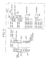
stage 30 with reference to FIG.11. The vector executestage 30 has the illustrated supervisory circuit for each of theload pipeline 150, thestore pipeline 151, theaddition pipeline 153, themultiplication pipeline 154 and thedivision pipeline 155. The following description relates to the structure of the supervisory circuit provided for the load pipeline 150 (a load supervisory circuit). The supervisory circuit is made up of a register (LRSR) 30-1, a register (LWSR) 30-2, counters 30-3, 30-4, and a logic circuit 30-5. A vector instruction supplied from thevector queue stage 29 is set in the register 30-1, which includes flag registers LRSR-VALID and LRSR-SU1. At the same time, the counter 30-3 is set to 0, and starts counting. Then, the vector instruction stored in the register 30-1 is supplied to theload pipeline 150 through thesignal line 160. When the counter 30-3 counts a value determined by the received vector instruction (read time), the vector instruction is read out of the register 30-1 and is then set in the register 30-2. At the same time, the counter 30-4 is set to "0", and then starts counting. When the counted value of the counter 30-4 reaches a value indicative of a time it takes to execute the vector instruction of concern (write time), the execution of the vector instruction is ended. - A circuit made of AND
gates 30a through 30d, inverters 30e, 30f, and ORgates system # 0 exists in either the register 30-1 or 30-2, the busy signal LSR-BUSY0 is "1". On the other hand, when a vector instruction relating tosystem # 1 exists in either the register 30-1 or 30-2, the busy signal LSR-BUSY1 is "1". - An
OR gate 30i included in the logic circuit 30-5 is supplied to busy signals LSR-BUSY0, SSR-BUSY0, ASR-BUSY0, MSR-BUSY0, and DSR-BUSY0 with respect to thepipelines control circuit 26. Similarly, an ORgates 30j generates a busy signal VES-BUSY1 from busy signals LSR-BUSY1, SSR-BUSY1, ASR-BUSY1, MSR-BUSY1, and DSR-BUSY1 with respect to thepipelines control circuit 26. - The present invention is not limited to the above-mentioned embodiment. For example, an arbitrary number of stages provided in the
vector control unit 16 may be used. The busy signal generated at each stage may be generated based only on whether one of thescalar units scalar units - The present invention is not limited to the above-mentioned embodiment, and variations and modification may be made without departing from the scope of the present invention.
Claims (21)
control stage means (4, 5, 7 - 9; 23, 24, 28 - 30) including a plurality of register stages used for controlling a pipeline process, for sequentially storing said second group of instructions relating to said selected one of said first execution units in said register stages and for outputting, for every register stage, a state indicating signal indicating state information on the corresponding register stage;
switching mode setting means (11, 27) for generating a mode setting signal used for selecting one of a plurality of switching modes (M1, M2, M3) each defining a timing with which the switching by said switching means is done; and
switching control means (10; 26) for generating said switching signal based on said state indicating signals output from said control stage means and said mode setting signal indicative of one of the plurality of switching modes supplied from said switching mode setting means.
said multiprocessor system comprises two first execution units (12, 13),
said switching control means (26) comprises first busy detecting means (26-1) relating to one (12) of said two first execution units, for determining whether or not the switching mode set by said switching mode setting means (27) can be done by referring to said state indicating signal supplied from each of said register stages (4, 5, 7 - 9; 23, 24, 28 - 30) and said switching mode setting signal supplied from said switching mode setting means (27) and for generating a first busy signal (BUSY0) indicative of the determination result, and second busy detecting means (26-2) relating to the other (13) of said two first execution units, for determining whether or not the switching mode set by said switching mode setting means (27) can be done by referring to said state indicating signal supplied from each of said register stages and said mode setting signal supplied from said switching mode setting means and for generating a second busy signal (BUSY1) indicative of the determination result, and
said first and second busy signals are supplied, as said switching signal, to said switching means.
a plurality of OR gates (31 - 33; 41 - 43) each performing an OR operation on said state indicating signals supplied from two or more register stages among said plurality of register stages, thereby outputting an OR operation result,
a plurality of AND gates (34 - 36; 44 - 46) respectively provided for said OR gates, each performing an AND operation on said OR operation result supplied from related one of said OR gates and one of said plurality of switching modes (M1, M2, M3), thereby outputting an AND operation result, and
an OR gate (37; 47) performing an OR operation on said AND operation results supplied from said plurality of AND gates, thereby outputting said first or second busy signal (BUSY0, BUSY1) to be supplied to said switching circuit.
said multiprocessor system comprises two first execution units (12, 13), and
said control stage means comprises first fetch register means (23), connected between one (12) of said first execution units and said switching means (25), for fetching said second group of instructions from said one of said first execution units, and
second fetch register means (24), connected between the other (13) of said first execution units and said switching means (25), for fetching said second group of instructions from the other of said first execution means.
first and second flip-flops (50, 51) each having set and reset terminals, first and second inverters (55, 56), first and second AND gates (52, 53), and an OR gates (54),
said first busy signal (BUSY0) is supplied, through said first inverter, to the reset terminal of said first flip-flop and the set terminal of said second flip-flop,
said second busy signal (BUSY1) is supplied, through said second inverter, to said set terminal of said first flip-flop and the reset terminal of said second flip-flop,
outputs of said first and second flip-flops (50, 51) are supplied to said first and second AND gates (52, 53), respectively, and said first and second AND gates are supplied with said second group of instructions relating to said respective first execution units first and second stages, and
outputs of said first and second AND gates are supplied to said OR gate (54), which outputs said second group of instructions related to said selected one of first execution units to said control stage means.
Applications Claiming Priority (2)
| Application Number | Priority Date | Filing Date | Title |
|---|---|---|---|
| JP140297/88 | 1988-06-07 | ||
| JP63140297A JPH06105460B2 (en) | 1988-06-07 | 1988-06-07 | Multiprocessor processor switching device |
Publications (3)
| Publication Number | Publication Date |
|---|---|
| EP0346003A2 true EP0346003A2 (en) | 1989-12-13 |
| EP0346003A3 EP0346003A3 (en) | 1991-06-05 |
| EP0346003B1 EP0346003B1 (en) | 1994-08-24 |
Family
ID=15265510
Family Applications (1)
| Application Number | Title | Priority Date | Filing Date |
|---|---|---|---|
| EP89305523A Expired - Lifetime EP0346003B1 (en) | 1988-06-07 | 1989-06-01 | Multiprocessor control system |
Country Status (5)
| Country | Link |
|---|---|
| US (1) | US5001627A (en) |
| EP (1) | EP0346003B1 (en) |
| JP (1) | JPH06105460B2 (en) |
| CA (1) | CA1315006C (en) |
| DE (1) | DE68917647T2 (en) |
Cited By (12)
| Publication number | Priority date | Publication date | Assignee | Title |
|---|---|---|---|---|
| WO2000067113A3 (en) * | 1999-04-29 | 2001-09-07 | Intel Corp | Method and apparatus for thread switching within a multithreaded processor |
| US6341347B1 (en) | 1999-05-11 | 2002-01-22 | Sun Microsystems, Inc. | Thread switch logic in a multiple-thread processor |
| US6357016B1 (en) | 1999-12-09 | 2002-03-12 | Intel Corporation | Method and apparatus for disabling a clock signal within a multithreaded processor |
| US6496925B1 (en) | 1999-12-09 | 2002-12-17 | Intel Corporation | Method and apparatus for processing an event occurrence within a multithreaded processor |
| US6542921B1 (en) | 1999-07-08 | 2003-04-01 | Intel Corporation | Method and apparatus for controlling the processing priority between multiple threads in a multithreaded processor |
| US6889319B1 (en) | 1999-12-09 | 2005-05-03 | Intel Corporation | Method and apparatus for entering and exiting multiple threads within a multithreaded processor |
| US7051329B1 (en) | 1999-12-28 | 2006-05-23 | Intel Corporation | Method and apparatus for managing resources in a multithreaded processor |
| US7127561B2 (en) | 2001-12-31 | 2006-10-24 | Intel Corporation | Coherency techniques for suspending execution of a thread until a specified memory access occurs |
| US7316021B2 (en) | 1999-05-11 | 2008-01-01 | Sun Microsystems, Inc. | Switching method in a multi-threaded processor |
| US7363474B2 (en) | 2001-12-31 | 2008-04-22 | Intel Corporation | Method and apparatus for suspending execution of a thread until a specified memory access occurs |
| US7856633B1 (en) | 2000-03-24 | 2010-12-21 | Intel Corporation | LRU cache replacement for a partitioned set associative cache |
| US8024735B2 (en) | 2002-06-14 | 2011-09-20 | Intel Corporation | Method and apparatus for ensuring fairness and forward progress when executing multiple threads of execution |
Families Citing this family (7)
| Publication number | Priority date | Publication date | Assignee | Title |
|---|---|---|---|---|
| JPH03233630A (en) * | 1990-02-08 | 1991-10-17 | Nec Corp | Information processor |
| US5261063A (en) * | 1990-12-07 | 1993-11-09 | Ibm Corp. | Pipeline apparatus having pipeline mode eecuting instructions from plural programs and parallel mode executing instructions from one of the plural programs |
| RU1804645C (en) * | 1991-03-27 | 1993-03-23 | Институт Точной Механики И Вычислительной Техники Им.С.А.Лебедева | Central processor |
| US5530881A (en) * | 1991-06-06 | 1996-06-25 | Hitachi, Ltd. | Vector processing apparatus for processing different instruction set architectures corresponding to mingled-type programs and separate-type programs |
| IT1264302B1 (en) * | 1993-12-24 | 1996-09-23 | Rainer Srl | MACHINE FOR THE PROCESSING OF A SHEET METAL. |
| US5663961A (en) * | 1995-02-24 | 1997-09-02 | Motorola, Inc. | Packet switch with centralized buffering for many output channels |
| US20250130799A1 (en) * | 2023-10-19 | 2025-04-24 | Ampere Computing Llc | Techniques for performing non-vector micro-operations on vector hardware |
Family Cites Families (7)
| Publication number | Priority date | Publication date | Assignee | Title |
|---|---|---|---|---|
| JPS5194734A (en) * | 1975-02-19 | 1976-08-19 | Tajushorisochino enzanseigyohoshiki | |
| JPS57155666A (en) * | 1981-03-20 | 1982-09-25 | Fujitsu Ltd | Instruction controlling system of vector processor |
| EP0105125B1 (en) * | 1982-09-03 | 1989-04-19 | Hitachi, Ltd. | Data processing system |
| KR900001999B1 (en) * | 1984-11-30 | 1990-03-31 | 후지쓰 가부시끼가이샤 | Multi processor system |
| US4875161A (en) * | 1985-07-31 | 1989-10-17 | Unisys Corporation | Scientific processor vector file organization |
| US4903196A (en) * | 1986-05-02 | 1990-02-20 | International Business Machines Corporation | Method and apparatus for guaranteeing the logical integrity of data in the general purpose registers of a complex multi-execution unit uniprocessor |
| US4760525A (en) * | 1986-06-10 | 1988-07-26 | The United States Of America As Represented By The Secretary Of The Air Force | Complex arithmetic vector processor for performing control function, scalar operation, and set-up of vector signal processing instruction |
-
1988
- 1988-06-07 JP JP63140297A patent/JPH06105460B2/en not_active Expired - Fee Related
-
1989
- 1989-06-01 DE DE68917647T patent/DE68917647T2/en not_active Expired - Fee Related
- 1989-06-01 EP EP89305523A patent/EP0346003B1/en not_active Expired - Lifetime
- 1989-06-06 CA CA000601891A patent/CA1315006C/en not_active Expired - Fee Related
- 1989-06-07 US US07/362,601 patent/US5001627A/en not_active Expired - Lifetime
Cited By (27)
| Publication number | Priority date | Publication date | Assignee | Title |
|---|---|---|---|---|
| US6850961B2 (en) | 1999-04-29 | 2005-02-01 | Intel Corporation | Method and system to perform a thread switching operation within a multithreaded processor based on detection of a stall condition |
| CN100399263C (en) * | 1999-04-29 | 2008-07-02 | 英特尔公司 | Method and apparatus for thread switching within multireaded processor |
| US6535905B1 (en) | 1999-04-29 | 2003-03-18 | Intel Corporation | Method and apparatus for thread switching within a multithreaded processor |
| WO2000067113A3 (en) * | 1999-04-29 | 2001-09-07 | Intel Corp | Method and apparatus for thread switching within a multithreaded processor |
| US6785890B2 (en) | 1999-04-29 | 2004-08-31 | Intel Corporation | Method and system to perform a thread switching operation within a multithreaded processor based on detection of the absence of a flow of instruction information for a thread |
| US6795845B2 (en) | 1999-04-29 | 2004-09-21 | Intel Corporation | Method and system to perform a thread switching operation within a multithreaded processor based on detection of a branch instruction |
| US6971104B2 (en) | 1999-04-29 | 2005-11-29 | Intel Corporation | Method and system to perform a thread switching operation within a multithreaded processor based on dispatch of a quantity of instruction information for a full instruction |
| US6854118B2 (en) | 1999-04-29 | 2005-02-08 | Intel Corporation | Method and system to perform a thread switching operation within a multithreaded processor based on detection of a flow marker within an instruction information |
| US6981261B2 (en) | 1999-04-29 | 2005-12-27 | Intel Corporation | Method and apparatus for thread switching within a multithreaded processor |
| US6865740B2 (en) | 1999-04-29 | 2005-03-08 | Intel Corporation | Method and system to insert a flow marker into an instruction stream to indicate a thread switching operation within a multithreaded processor |
| US6341347B1 (en) | 1999-05-11 | 2002-01-22 | Sun Microsystems, Inc. | Thread switch logic in a multiple-thread processor |
| WO2000068780A3 (en) * | 1999-05-11 | 2002-05-10 | Sun Microsystems Inc | Thread switch logic in a multiple-thread processor |
| US7316021B2 (en) | 1999-05-11 | 2008-01-01 | Sun Microsystems, Inc. | Switching method in a multi-threaded processor |
| US6542921B1 (en) | 1999-07-08 | 2003-04-01 | Intel Corporation | Method and apparatus for controlling the processing priority between multiple threads in a multithreaded processor |
| US6928647B2 (en) | 1999-07-08 | 2005-08-09 | Intel Corporation | Method and apparatus for controlling the processing priority between multiple threads in a multithreaded processor |
| US6496925B1 (en) | 1999-12-09 | 2002-12-17 | Intel Corporation | Method and apparatus for processing an event occurrence within a multithreaded processor |
| US6857064B2 (en) | 1999-12-09 | 2005-02-15 | Intel Corporation | Method and apparatus for processing events in a multithreaded processor |
| US7039794B2 (en) | 1999-12-09 | 2006-05-02 | Intel Corporation | Method and apparatus for processing an event occurrence for a least one thread within a multithreaded processor |
| US6889319B1 (en) | 1999-12-09 | 2005-05-03 | Intel Corporation | Method and apparatus for entering and exiting multiple threads within a multithreaded processor |
| US7353370B2 (en) | 1999-12-09 | 2008-04-01 | Intel Corporation | Method and apparatus for processing an event occurrence within a multithreaded processor |
| US7366879B2 (en) | 1999-12-09 | 2008-04-29 | Intel Corporation | Alteration of functional unit partitioning scheme in multithreaded processor based upon thread statuses |
| US6357016B1 (en) | 1999-12-09 | 2002-03-12 | Intel Corporation | Method and apparatus for disabling a clock signal within a multithreaded processor |
| US7051329B1 (en) | 1999-12-28 | 2006-05-23 | Intel Corporation | Method and apparatus for managing resources in a multithreaded processor |
| US7856633B1 (en) | 2000-03-24 | 2010-12-21 | Intel Corporation | LRU cache replacement for a partitioned set associative cache |
| US7127561B2 (en) | 2001-12-31 | 2006-10-24 | Intel Corporation | Coherency techniques for suspending execution of a thread until a specified memory access occurs |
| US7363474B2 (en) | 2001-12-31 | 2008-04-22 | Intel Corporation | Method and apparatus for suspending execution of a thread until a specified memory access occurs |
| US8024735B2 (en) | 2002-06-14 | 2011-09-20 | Intel Corporation | Method and apparatus for ensuring fairness and forward progress when executing multiple threads of execution |
Also Published As
| Publication number | Publication date |
|---|---|
| JPH06105460B2 (en) | 1994-12-21 |
| EP0346003A3 (en) | 1991-06-05 |
| DE68917647T2 (en) | 1994-12-22 |
| DE68917647D1 (en) | 1994-09-29 |
| JPH01309178A (en) | 1989-12-13 |
| EP0346003B1 (en) | 1994-08-24 |
| US5001627A (en) | 1991-03-19 |
| CA1315006C (en) | 1993-03-23 |
Similar Documents
| Publication | Publication Date | Title |
|---|---|---|
| EP0346003B1 (en) | Multiprocessor control system | |
| US5881302A (en) | Vector processing unit with reconfigurable data buffer | |
| US4214305A (en) | Multi-processor data processing system | |
| US5241679A (en) | Data processor for executing data saving and restoration register and data saving stack with corresponding stack storage for each register | |
| US4984151A (en) | Flexible, next-address generation microprogram sequencer | |
| US5060148A (en) | Control system for vector processor with serialization instruction for memory accesses for pipeline operation | |
| EP0087978A2 (en) | Information processing unit | |
| US4308581A (en) | Single step system for a microcomputer | |
| US5497496A (en) | Superscalar processor controlling fetching of instructions based upon number of empty instructions registers detected for each cycle | |
| EP0126247B1 (en) | Computer system | |
| JPH0332818B2 (en) | ||
| US4777592A (en) | Information processing system comprising a register renewal waiting control circuit with renewal register number registering means | |
| EP0223150B1 (en) | Information processing apparatus | |
| EP0167959B1 (en) | Computer vector register processing | |
| US4837688A (en) | Multi-channel shared resource processor | |
| EP0346031A2 (en) | Vector data processing apparatus | |
| EP0437207A2 (en) | Information processing system | |
| AU626067B2 (en) | Apparatus and method for control of asynchronous program interrupt events in a data processing system | |
| US5050076A (en) | Prefetching queue control system | |
| KR900005284B1 (en) | Micro computer | |
| EP0700005B1 (en) | Vector data bypass mechanism for vector computer | |
| KR100249536B1 (en) | Data processor having bus controller for controlling a plurality of buses independently of each other | |
| EP0416345B1 (en) | Instruction decoder for a pipeline processor | |
| AU691593B2 (en) | Vector processing unit with reconfigurable data buffer | |
| JPH0222413B2 (en) |
Legal Events
| Date | Code | Title | Description |
|---|---|---|---|
| PUAI | Public reference made under article 153(3) epc to a published international application that has entered the european phase |
Free format text: ORIGINAL CODE: 0009012 |
|
| AK | Designated contracting states |
Kind code of ref document: A2 Designated state(s): DE FR GB |
|
| PUAL | Search report despatched |
Free format text: ORIGINAL CODE: 0009013 |
|
| AK | Designated contracting states |
Kind code of ref document: A3 Designated state(s): DE FR GB |
|
| 17P | Request for examination filed |
Effective date: 19910731 |
|
| 17Q | First examination report despatched |
Effective date: 19930311 |
|
| GRAA | (expected) grant |
Free format text: ORIGINAL CODE: 0009210 |
|
| AK | Designated contracting states |
Kind code of ref document: B1 Designated state(s): DE FR GB |
|
| REF | Corresponds to: |
Ref document number: 68917647 Country of ref document: DE Date of ref document: 19940929 |
|
| ET | Fr: translation filed | ||
| PLBE | No opposition filed within time limit |
Free format text: ORIGINAL CODE: 0009261 |
|
| STAA | Information on the status of an ep patent application or granted ep patent |
Free format text: STATUS: NO OPPOSITION FILED WITHIN TIME LIMIT |
|
| 26N | No opposition filed | ||
| REG | Reference to a national code |
Ref country code: GB Ref legal event code: IF02 |
|
| PGFP | Annual fee paid to national office [announced via postgrant information from national office to epo] |
Ref country code: DE Payment date: 20060525 Year of fee payment: 18 |
|
| PGFP | Annual fee paid to national office [announced via postgrant information from national office to epo] |
Ref country code: GB Payment date: 20060531 Year of fee payment: 18 |
|
| PGFP | Annual fee paid to national office [announced via postgrant information from national office to epo] |
Ref country code: FR Payment date: 20060608 Year of fee payment: 18 |
|
| GBPC | Gb: european patent ceased through non-payment of renewal fee |
Effective date: 20070601 |
|
| REG | Reference to a national code |
Ref country code: FR Ref legal event code: ST Effective date: 20080229 |
|
| PG25 | Lapsed in a contracting state [announced via postgrant information from national office to epo] |
Ref country code: DE Free format text: LAPSE BECAUSE OF NON-PAYMENT OF DUE FEES Effective date: 20080101 |
|
| PG25 | Lapsed in a contracting state [announced via postgrant information from national office to epo] |
Ref country code: GB Free format text: LAPSE BECAUSE OF NON-PAYMENT OF DUE FEES Effective date: 20070601 |
|
| PG25 | Lapsed in a contracting state [announced via postgrant information from national office to epo] |
Ref country code: FR Free format text: LAPSE BECAUSE OF NON-PAYMENT OF DUE FEES Effective date: 20070702 |