EP0345086A1 - Einkristall-Ausgangsbildschirm - Google Patents
Einkristall-Ausgangsbildschirm Download PDFInfo
- Publication number
- EP0345086A1 EP0345086A1 EP89305587A EP89305587A EP0345086A1 EP 0345086 A1 EP0345086 A1 EP 0345086A1 EP 89305587 A EP89305587 A EP 89305587A EP 89305587 A EP89305587 A EP 89305587A EP 0345086 A1 EP0345086 A1 EP 0345086A1
- Authority
- EP
- European Patent Office
- Prior art keywords
- output screen
- stage
- semiconductor
- photocathode
- layer
- Prior art date
- Legal status (The legal status is an assumption and is not a legal conclusion. Google has not performed a legal analysis and makes no representation as to the accuracy of the status listed.)
- Withdrawn
Links
- 239000013078 crystal Substances 0.000 title claims abstract description 20
- 239000004065 semiconductor Substances 0.000 claims abstract description 29
- 150000001875 compounds Chemical class 0.000 claims abstract description 16
- 230000006798 recombination Effects 0.000 claims abstract description 6
- 238000005215 recombination Methods 0.000 claims abstract description 6
- 229910001218 Gallium arsenide Inorganic materials 0.000 claims description 19
- 229910000980 Aluminium gallium arsenide Inorganic materials 0.000 claims description 10
- 239000000463 material Substances 0.000 claims description 9
- 239000002245 particle Substances 0.000 claims description 4
- -1 GaAsP Inorganic materials 0.000 claims description 2
- 229910000530 Gallium indium arsenide Inorganic materials 0.000 claims description 2
- 239000000969 carrier Substances 0.000 claims description 2
- 230000015556 catabolic process Effects 0.000 claims description 2
- 238000006731 degradation reaction Methods 0.000 claims description 2
- 230000005540 biological transmission Effects 0.000 claims 1
- 230000002708 enhancing effect Effects 0.000 claims 1
- 230000003287 optical effect Effects 0.000 abstract description 4
- 230000008878 coupling Effects 0.000 abstract description 3
- 238000010168 coupling process Methods 0.000 abstract description 3
- 238000005859 coupling reaction Methods 0.000 abstract description 3
- 239000010410 layer Substances 0.000 description 55
- JBRZTFJDHDCESZ-UHFFFAOYSA-N AsGa Chemical compound [As]#[Ga] JBRZTFJDHDCESZ-UHFFFAOYSA-N 0.000 description 19
- OAICVXFJPJFONN-UHFFFAOYSA-N Phosphorus Chemical compound [P] OAICVXFJPJFONN-UHFFFAOYSA-N 0.000 description 12
- 238000000034 method Methods 0.000 description 9
- 150000002500 ions Chemical class 0.000 description 7
- 239000000758 substrate Substances 0.000 description 7
- 229910052782 aluminium Inorganic materials 0.000 description 5
- XAGFODPZIPBFFR-UHFFFAOYSA-N aluminium Chemical compound [Al] XAGFODPZIPBFFR-UHFFFAOYSA-N 0.000 description 5
- 230000004888 barrier function Effects 0.000 description 4
- 230000000694 effects Effects 0.000 description 4
- 238000004519 manufacturing process Methods 0.000 description 4
- 230000007547 defect Effects 0.000 description 3
- 239000011521 glass Substances 0.000 description 3
- 239000004922 lacquer Substances 0.000 description 3
- 230000008569 process Effects 0.000 description 3
- 230000004044 response Effects 0.000 description 3
- 238000001228 spectrum Methods 0.000 description 3
- 238000005253 cladding Methods 0.000 description 2
- 230000005684 electric field Effects 0.000 description 2
- 230000007935 neutral effect Effects 0.000 description 2
- 230000004297 night vision Effects 0.000 description 2
- 230000000737 periodic effect Effects 0.000 description 2
- 230000035945 sensitivity Effects 0.000 description 2
- 239000002002 slurry Substances 0.000 description 2
- 230000003595 spectral effect Effects 0.000 description 2
- 238000010521 absorption reaction Methods 0.000 description 1
- 229910045601 alloy Inorganic materials 0.000 description 1
- 239000000956 alloy Substances 0.000 description 1
- 230000003321 amplification Effects 0.000 description 1
- 239000006117 anti-reflective coating Substances 0.000 description 1
- 229910052792 caesium Inorganic materials 0.000 description 1
- TVFDJXOCXUVLDH-UHFFFAOYSA-N caesium atom Chemical compound [Cs] TVFDJXOCXUVLDH-UHFFFAOYSA-N 0.000 description 1
- 229910001942 caesium oxide Inorganic materials 0.000 description 1
- 238000006243 chemical reaction Methods 0.000 description 1
- 238000005229 chemical vapour deposition Methods 0.000 description 1
- 239000011248 coating agent Substances 0.000 description 1
- 238000000576 coating method Methods 0.000 description 1
- 239000000356 contaminant Substances 0.000 description 1
- 238000011109 contamination Methods 0.000 description 1
- 230000009849 deactivation Effects 0.000 description 1
- 230000000593 degrading effect Effects 0.000 description 1
- 230000001419 dependent effect Effects 0.000 description 1
- 238000009792 diffusion process Methods 0.000 description 1
- 239000002019 doping agent Substances 0.000 description 1
- 238000005530 etching Methods 0.000 description 1
- 238000003384 imaging method Methods 0.000 description 1
- 229910052738 indium Inorganic materials 0.000 description 1
- APFVFJFRJDLVQX-UHFFFAOYSA-N indium atom Chemical compound [In] APFVFJFRJDLVQX-UHFFFAOYSA-N 0.000 description 1
- 229910052751 metal Inorganic materials 0.000 description 1
- 239000002184 metal Substances 0.000 description 1
- 239000000203 mixture Substances 0.000 description 1
- 238000003199 nucleic acid amplification method Methods 0.000 description 1
- 230000002688 persistence Effects 0.000 description 1
- 231100000572 poisoning Toxicity 0.000 description 1
- 230000000607 poisoning effect Effects 0.000 description 1
- 239000000843 powder Substances 0.000 description 1
- 239000002904 solvent Substances 0.000 description 1
- 238000004544 sputter deposition Methods 0.000 description 1
- 230000005641 tunneling Effects 0.000 description 1
Images
Classifications
-
- H—ELECTRICITY
- H01—ELECTRIC ELEMENTS
- H01J—ELECTRIC DISCHARGE TUBES OR DISCHARGE LAMPS
- H01J29/00—Details of cathode-ray tubes or of electron-beam tubes of the types covered by group H01J31/00
- H01J29/02—Electrodes; Screens; Mounting, supporting, spacing or insulating thereof
- H01J29/10—Screens on or from which an image or pattern is formed, picked up, converted or stored
-
- H—ELECTRICITY
- H01—ELECTRIC ELEMENTS
- H01J—ELECTRIC DISCHARGE TUBES OR DISCHARGE LAMPS
- H01J31/00—Cathode ray tubes; Electron beam tubes
- H01J31/08—Cathode ray tubes; Electron beam tubes having a screen on or from which an image or pattern is formed, picked up, converted, or stored
- H01J31/50—Image-conversion or image-amplification tubes, i.e. having optical, X-ray, or analogous input, and optical output
-
- H—ELECTRICITY
- H10—SEMICONDUCTOR DEVICES; ELECTRIC SOLID-STATE DEVICES NOT OTHERWISE PROVIDED FOR
- H10H—INORGANIC LIGHT-EMITTING SEMICONDUCTOR DEVICES HAVING POTENTIAL BARRIERS
- H10H20/00—Individual inorganic light-emitting semiconductor devices having potential barriers, e.g. light-emitting diodes [LED]
- H10H20/80—Constructional details
- H10H20/81—Bodies
- H10H20/811—Bodies having quantum effect structures or superlattices, e.g. tunnel junctions
-
- H—ELECTRICITY
- H10—SEMICONDUCTOR DEVICES; ELECTRIC SOLID-STATE DEVICES NOT OTHERWISE PROVIDED FOR
- H10H—INORGANIC LIGHT-EMITTING SEMICONDUCTOR DEVICES HAVING POTENTIAL BARRIERS
- H10H20/00—Individual inorganic light-emitting semiconductor devices having potential barriers, e.g. light-emitting diodes [LED]
- H10H20/80—Constructional details
- H10H20/81—Bodies
- H10H20/822—Materials of the light-emitting regions
- H10H20/824—Materials of the light-emitting regions comprising only Group III-V materials, e.g. GaP
-
- H—ELECTRICITY
- H01—ELECTRIC ELEMENTS
- H01J—ELECTRIC DISCHARGE TUBES OR DISCHARGE LAMPS
- H01J2231/00—Cathode ray tubes or electron beam tubes
- H01J2231/50—Imaging and conversion tubes
- H01J2231/50057—Imaging and conversion tubes characterised by form of output stage
- H01J2231/50063—Optical
Definitions
- This invention is in the field of light output vacuum tubes and particularly relates to the output screen of a vacuum tube whereby electrons are converted to light.
- a variety of vacuum tubes are designed to produce a light output by converting a flow of electrons into photons at an output screen.
- the light output forms an image, displays a signal or signals an event, i.e., acts as a detector or counter.
- Well known examples of such tubes include cathode ray tubes, x-ray image intensifier tubes, infrared detectors and night vision tubes.
- the term light output is intended to include the output of photons in the infrared region of the electromagnetic spectrum.
- the input signal in many types of such tubes also consists of photons which are converted into electrons at a photocathode and amplified before being converted back to photons at the output screen.
- Such tubes may be designed for sensitivity to input photons which are in a different region of the spectrum than the output photons.
- Certain image intensifiers and detector tubes now employ input photocathodes comprising Gallium Arsenide (GaAs) or other III-V semiconductor compounds. While photocathodes comprising III-V semiconductor compounds offer advantages which make them indispensable in certain applications, they are particularly susceptible to contamination by ions and neutral gas molecules which may be released in the vacuum tube during normal operation. Since the photocathode is negatively biased, any positive ions present in the tube will be attracted towards it. Bombardment of the photocathode by such ions create crystal defects in the semiconductor layer, and sputters away both the cesium/cesium oxide layers and semiconductor layers ultimately destroying the photocathode. Tube life may be rendered unacceptably short by these effects.
- GaAs Gallium Arsenide
- ion feedback is a source of noise.
- a large number of secondary electrons are produced. These electrons are then accelerated back into the screen where they show up as a flash of light. These flashes or scintillations are a significant source of noise in proximity focused image intensifiers.
- the output screens of light output vacuum tubes are traditionally made of a "phosphor.”
- phosphor There are a large number of commercially available phosphor materials with well-known and well described properties.
- the tube designer is interested in selecting one which offers a desired efficiency, color (i.e., spectral characteristics), response time and persistence.
- the phosphor output screen is typically made by applying a slurry comprising uniformly sized particles of the phosphor material(s) suspended in a solvent to a glass window which forms a part of the vacuum envelop.
- a slurry comprising uniformly sized particles of the phosphor material(s) suspended in a solvent
- a lacquer may be applied to the output window and then brush the dry phosphor powder onto the wet lacquer. While these are relatively easy processes, it is difficult to precisely control the uniformity of the resulting phosphor film.
- Phosphor screens of the type described have gained almost universal application because they are easy to manufacture, can be selected to offer a desired spectral response and offer high efficiency conversion of electrons to output photons. It should be noted, however, that high efficiency typically comes at a cost of slower response time.
- the traditional phosphor screens even when coated with a layer of aluminum, release unacceptably high numbers of ions and neutral gas particles when used in a diode tube employing a GaAs or other III-V compound input photocathode.
- Normal vacuum tube manufacturing techniques such as long tube pump downs and bake outs do not entirely eliminate the problem.
- the phosphor screens comprising a very large number of individual particles, have a very large relative surface area.
- an output screen as set out in Claim 1.
- the invention provides in another aspect a vacuum tube comprising a photocathode and such an output screen which emitts photons when struck by the electrons emitted by the photocathode as set out in Claim 9.
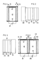
- FIG. 1 is a schematic representation of a diode 10 which may be used either as a photodetector or as a simple proximity focused image intensifier.
- Diode 10 comprises an input window 20 which should be transparent to photons in the range of wavelengths of interest. After passing through the input window 20 these photons are absorbed and converted to electrons in photocathode 25.
- the present invention is particularly useful in tubes wherein the photocathode comprises a crystal of GaAs, InGaAs or other III-V semiconductor compounds which are highly susceptible to "poisoning" or deactivation in the presence of contaminants.
- III-V semiconductor should be understood to mean a crystalline alloy or compound substantially consisting of atoms of one or more of the elements in column III of the periodic table and a substantially equal number of atoms of one or more of the elements in column V of the periodic table.
- semiconductor crystals can be grown by a variety of known techniques, including, for example, metal organic chemical vapor deposition (MOCVD) and are typically doped by well known methods. Examples of such photocathodes and of methods of making them are described in U.S. Pat. Nos. 3,644,770 and 3,959,045.
- Electrons are emitted from the photocathode 25, enter the vacuum space within the tube 10 and are accelerated toward the output screen 30 by an electric field applied between photocathode 25 and output screen 30 by power supply 50.
- power supply 50 may provide a forward bias in the range of 10-20 Kv.
- Window 35 is transparent to photons of the wavelength(s) emitted by the output screen and may be plain glass or a fiberoptic plate. In either case the output window 30 may be optically coupled to a second stage device such as a photomultiplier tube, an image intensifier or a charged coupled device.
- a second stage device such as a photomultiplier tube, an image intensifier or a charged coupled device.
- the energy gained by the electrons in transitting the interior of the tube is responsible for the overall gain of the tube. After being accelerated by the electric field in the tube, a single electron emitted by the photocathode may, in turn, release hundreds of photons in the output screen.
- the vacuum envelop for tube 10 is completed by walls 40 which also serve to insulate the photocathode 25 from the output screen 30.
- the overall shape of the tube 10 typically will be cylindrical.
- the resulting structure is then bonded to output window 35 and the layers 100, 105, 110, and 115 are removed by lapping and etching.
- a process for bonding the photocathode to the output window is described in U.S. Pat. No. 3,769,536. Two etch-stop layers are used in order to gain better control and precision in removing the right amount of material.
- an aluminum film 150 (shown in FIG. 3) is deposited onto the first AlGaAs etch-stop/cap layer by sputter coating.
- the purpose of the aluminum film 150 is to prevent light emitted in the output screen 30 from reaching the photocathode 25 where it cculd cause spurious emission of electrons and create an undesired feedback loop.
- the aluminum layer 150 is, therefore, thick enough to be optically reflective but thin enough to permit the electrons emitted from the photocathode to reach the active region of the output screen 30 without losing a significant amount of energy.
- FIG. 3 shows the resulting output screen structure 30 mounted on output window 35.
- the active portion of the output screen consists of GaAs layer 125 and AlGaAs cap layers 120 and 130.
- AlGaAs layer 120 is relatively thin, again thin enough to allow electrons to pass through it unabsorbed. Electrons which pass through layer 150 and layer 120 are absorbed in GaAs layer 125. As an electron is absorbed it generates a large number of electron hole pairs. The number of electron hole pairs created is a function of the energy of the incident electron. Recombination of these pairs results in isotropic photon emission at the bandgap frequency of GaAs, which is in the infrared region of the spectrum.
- ternary or quaternary compounds such as InGaAsP or InGaP, one can achieve both good lattice matching and a desired bandgap frequency.
- the output screen structure 30 minimizes efficiency losses due to non-radiative recombination of electrons or holes at the surface of the GaAs layer.
- a crystal surface has a high population of electronically active defects which are responsible for non-radiative recombination.
- lattice matched cap layers 120 and 130 minimizes the presence of these defects in the active region of the output screen.
- the interface between active layer 125 and cap layers 120 and 130 is not a crystal surface, although the interface serves as a confining layer for the electrons and holes.
- the cladding layers 120 and 130 In order to provide effective minority carrier confinement, the cladding layers 120 and 130 must have the following properties: 1) their bandgap must be of greater energy than that of the active layer 125; 2) the layers must be doped in the same manner as the active layer 125; 3) the cladding layers must be thicker than the characteristic tunneling distance, i.e., 200 ⁇ should be sufficient. It should also be noted that AlGaAs layers 120 and 130 are transparent to light emitted in active GaAs layer 125. When using an active layer of a different semiconductor compound, the composition of the cap layers should, likewise, be selected to both be lattice matched to the active layer and transparent to light emitted by the active layer.
- etch-stop/cap layer 120 is removed and does not become a part of the final structure. Instead, by diffusion doping the GaAs layer 125 a doping profile is created which accelerates the minority carriers away from the crystal surface where they are subject to non-radiative recombination. Methods of creating a doping profile useful in this embodiment are well known in the art.
- Light cannot exit the photocathode 30 into a medium with a lower index of refraction if the angle of incidence at the interface between the materials exceeds the "critical" angle.
- GaAs has a relatively high index of refraction. However, this is not a serious problem in transmitting light from the GaAs layer into the AlGaAs cap layer 130 because it has an index of refraction similar to GaAs. However, glass has a much lower index of refraction and consequently the critical angle becomes much smaller at that interface.
- One way of avoiding this limitation is to roughen or texture the interface in question thereby increasing the opportunity for the light to strike the surface at an angle less than the critical angle.
- FIG. 4 shows another approach to avoiding the limitation associated with getting light out of a material having a high index of refraction when the light emitted by the output screen is to be coupled into a second stage tube for further signal amplification.
- Tube 210 is a two-stage device with each stage comprising essentially the same elements as the FIG. 1 tube 10 except as discussed below.
- Tube 210 is divided into its two parts by optical coupling/support member 200.
- Member 200 supports the output screen 30 of the first stage of the tube, which is the same as described above, and photocathode 225, which is the input for the second stage of the tube. Note that member 200 does not serve as any part of the vacuum envelop for the tube and, thus, need not have great strength or thickness.
- member 200 is a thin substrate, like GaAs, upon which the active layers of output screen 30 and photocathode 225 may be grown directly, simplifying the manufacturing process.
- the substrate material 200 must be transparent to the light generated in layer 30.
- the effective bandgap of this substrate can be slightly shifted by the use of dopants.
- the preferred embodiment of this structure makes use of this effect in that layer 30 would contain a P doped active layer whereas the substrate would be undoped or N doped.
- the active layer of the photocathode, layer 225 would contain a small percentage of Indium to enhance optical absorption of the light generated in layer 30. It should also be noted that if the substrate could be extremely thin, this device would have imaging applications.
- output screen 30, support member 200 and photocathode 225 all have substantially the same index of refraction, the optical coupling between the stages is excellent and light loss due to the critical angle effect is minimized. Needless to say, there is no need to stop at two stages; an integral tube comprising a plurality of stages can be constructed in this manner.
- the two stages of tube 210 are shown to be alike this is not necessary.
- the second stage could be a photomultiplier tube incorporating a microchannel plate. It is known that the noise figure for a photomultiplier tube is highly dependent on the gain of the first stage. By using a first stage detector of the type described herein, a high gain can be achieved lowering the overall noise of the system.
- the second stage could contain a microchannel plate followed by a standard phosphor screen.
Landscapes
- Common Detailed Techniques For Electron Tubes Or Discharge Tubes (AREA)
- Image-Pickup Tubes, Image-Amplification Tubes, And Storage Tubes (AREA)
Applications Claiming Priority (2)
| Application Number | Priority Date | Filing Date | Title |
|---|---|---|---|
| US07/202,640 US4929867A (en) | 1988-06-03 | 1988-06-03 | Two stage light converting vacuum tube |
| US202640 | 1988-06-03 |
Publications (1)
| Publication Number | Publication Date |
|---|---|
| EP0345086A1 true EP0345086A1 (de) | 1989-12-06 |
Family
ID=22750714
Family Applications (1)
| Application Number | Title | Priority Date | Filing Date |
|---|---|---|---|
| EP89305587A Withdrawn EP0345086A1 (de) | 1988-06-03 | 1989-06-02 | Einkristall-Ausgangsbildschirm |
Country Status (2)
| Country | Link |
|---|---|
| US (1) | US4929867A (de) |
| EP (1) | EP0345086A1 (de) |
Cited By (1)
| Publication number | Priority date | Publication date | Assignee | Title |
|---|---|---|---|---|
| EP4376044A1 (de) * | 2022-11-22 | 2024-05-29 | L3Harris Technologies, Inc. | Entwurf von gitterangepassten photokathoden für erweiterte wellenlängen |
Families Citing this family (2)
| Publication number | Priority date | Publication date | Assignee | Title |
|---|---|---|---|---|
| US6338663B1 (en) * | 1998-05-14 | 2002-01-15 | Micron Technology, Inc. | Low-voltage cathode for scrubbing cathodoluminescent layers for field emission displays and method |
| US20080121270A1 (en) * | 2006-11-28 | 2008-05-29 | General Electric Company | Photovoltaic roof tile system |
Citations (5)
| Publication number | Priority date | Publication date | Assignee | Title |
|---|---|---|---|---|
| US3571646A (en) * | 1967-07-17 | 1971-03-23 | Tokyo Shibaura Electric Co | Photoconductive target with n-type layer of cadmium selenide including cadmium chloride and cuprous chloride |
| GB1298877A (en) * | 1969-02-27 | 1972-12-06 | Philips Electronic Associated | Electronic discharge tube including an electron-emissive electrode which comprises an activated p-type semiconductor |
| GB1344859A (en) * | 1970-01-19 | 1974-01-23 | Varian Associates | Multilayered group iii-v material having a high quality active layer |
| GB1427209A (en) * | 1972-09-22 | 1976-03-10 | Varian Associates | Lattice matched heterojunction devices |
| US3959045A (en) * | 1974-11-18 | 1976-05-25 | Varian Associates | Process for making III-V devices |
Family Cites Families (8)
| Publication number | Priority date | Publication date | Assignee | Title |
|---|---|---|---|---|
| DE757713C (de) * | 1939-06-25 | 1953-09-07 | Licentia Gmbh | Einrichtung zur Erzeugung sichtbarer oder photographischer Bilder von Koerpern unterVerwendung einer Neutronenstrahlenquelle |
| US3644770A (en) * | 1968-01-18 | 1972-02-22 | Varian Associates | Photoemitter having a p-type semiconductive substrate overlaid with cesium and n-type cesium oxide layers |
| US3575628A (en) * | 1968-11-26 | 1971-04-20 | Westinghouse Electric Corp | Transmissive photocathode and devices utilizing the same |
| US3696262A (en) * | 1970-01-19 | 1972-10-03 | Varian Associates | Multilayered iii-v photocathode having a transition layer and a high quality active layer |
| US3699401A (en) * | 1971-05-17 | 1972-10-17 | Rca Corp | Photoemissive electron tube comprising a thin film transmissive semiconductor photocathode structure |
| US3769536A (en) * | 1972-01-28 | 1973-10-30 | Varian Associates | Iii-v photocathode bonded to a foreign transparent substrate |
| SU736212A1 (ru) * | 1977-12-15 | 1980-05-25 | Предприятие П/Я Г-4294 | Многокамерный усилитель ркости изображени |
| US4626694A (en) * | 1983-12-23 | 1986-12-02 | Tokyo Shibaura Denki Kabushiki Kaisha | Image intensifier |
-
1988
- 1988-06-03 US US07/202,640 patent/US4929867A/en not_active Expired - Lifetime
-
1989
- 1989-06-02 EP EP89305587A patent/EP0345086A1/de not_active Withdrawn
Patent Citations (5)
| Publication number | Priority date | Publication date | Assignee | Title |
|---|---|---|---|---|
| US3571646A (en) * | 1967-07-17 | 1971-03-23 | Tokyo Shibaura Electric Co | Photoconductive target with n-type layer of cadmium selenide including cadmium chloride and cuprous chloride |
| GB1298877A (en) * | 1969-02-27 | 1972-12-06 | Philips Electronic Associated | Electronic discharge tube including an electron-emissive electrode which comprises an activated p-type semiconductor |
| GB1344859A (en) * | 1970-01-19 | 1974-01-23 | Varian Associates | Multilayered group iii-v material having a high quality active layer |
| GB1427209A (en) * | 1972-09-22 | 1976-03-10 | Varian Associates | Lattice matched heterojunction devices |
| US3959045A (en) * | 1974-11-18 | 1976-05-25 | Varian Associates | Process for making III-V devices |
Cited By (2)
| Publication number | Priority date | Publication date | Assignee | Title |
|---|---|---|---|---|
| EP4376044A1 (de) * | 2022-11-22 | 2024-05-29 | L3Harris Technologies, Inc. | Entwurf von gitterangepassten photokathoden für erweiterte wellenlängen |
| US12308198B2 (en) | 2022-11-22 | 2025-05-20 | L3Harris Technologies, Inc. | Lattice matched photocathodes for extended wavelengths |
Also Published As
| Publication number | Publication date |
|---|---|
| US4929867A (en) | 1990-05-29 |
Similar Documents
| Publication | Publication Date | Title |
|---|---|---|
| Martinelli et al. | The application of semiconductors with negative electron affinity surfaces to electron emission devices | |
| US5354694A (en) | Method of making highly doped surface layer for negative electron affinity devices | |
| US5268570A (en) | Transmission mode InGaAs photocathode for night vision system | |
| EP0521626B1 (de) | Mikrokanalplatte mit begrenzter Rückkopplung | |
| EP0642147B1 (de) | Photoemitter, Elektronenröhre, und Photodetektor | |
| US5677923A (en) | Vertical cavity electron beam pumped semiconductor lasers and methods | |
| EP0746871A1 (de) | Photonen- oder teilchendetektor, herstellungsverfahren des detektors und messverfahren | |
| Pollehn | Performance and reliability of third-generation image intensifies | |
| US6998635B2 (en) | Tuned bandwidth photocathode for transmission negative electron affinity devices | |
| US20020067750A1 (en) | Electron beam pumped semiconductor laser screen and associated fabrication method | |
| JP4996028B2 (ja) | 強化コーティングを有するマイクロチャネルプレート | |
| US6005257A (en) | Transmission mode photocathode with multilayer active layer for night vision and method | |
| EP0721654B1 (de) | Bildverstärkerröhre | |
| WO1996004675A1 (en) | TRANSMISSION MODE 1.06νM PHOTOCATHODE FOR NIGHT VISION AND METHOD | |
| US3951698A (en) | Dual use of epitaxy seed crystal as tube input window and cathode structure base | |
| US6116976A (en) | Photocathode and image intensifier tube having an active layer comprised substantially of amorphic diamond-like carbon, diamond, or a combination of both | |
| US4929867A (en) | Two stage light converting vacuum tube | |
| Seib et al. | Photodetectors for the 0.1 to 1.0 μm Spectral Region | |
| KR100423849B1 (ko) | 매우 얇은 보호막을 갖는 광음극 | |
| US4019082A (en) | Electron emitting device and method of making the same | |
| US6069445A (en) | Having an electrical contact on an emission surface thereof | |
| US7462090B1 (en) | Method and system for detecting radiation incorporating a hardened photocathode | |
| Sommer | Practical use of III-V compound electron emitters | |
| CA3075509C (en) | Thermally assisted negative electron affinity photocathode | |
| Pollehn | Image intensifiers |
Legal Events
| Date | Code | Title | Description |
|---|---|---|---|
| PUAI | Public reference made under article 153(3) epc to a published international application that has entered the european phase |
Free format text: ORIGINAL CODE: 0009012 |
|
| AK | Designated contracting states |
Kind code of ref document: A1 Designated state(s): DE FR GB NL |
|
| 17P | Request for examination filed |
Effective date: 19900404 |
|
| 17Q | First examination report despatched |
Effective date: 19911227 |
|
| STAA | Information on the status of an ep patent application or granted ep patent |
Free format text: STATUS: THE APPLICATION IS DEEMED TO BE WITHDRAWN |
|
| 18D | Application deemed to be withdrawn |
Effective date: 19921023 |