EP0345050A2 - Thermal imaging device - Google Patents
Thermal imaging device Download PDFInfo
- Publication number
- EP0345050A2 EP0345050A2 EP89305499A EP89305499A EP0345050A2 EP 0345050 A2 EP0345050 A2 EP 0345050A2 EP 89305499 A EP89305499 A EP 89305499A EP 89305499 A EP89305499 A EP 89305499A EP 0345050 A2 EP0345050 A2 EP 0345050A2
- Authority
- EP
- European Patent Office
- Prior art keywords
- layer
- tongues
- pyroelectric
- array
- contacts
- Prior art date
- Legal status (The legal status is an assumption and is not a legal conclusion. Google has not performed a legal analysis and makes no representation as to the accuracy of the status listed.)
- Granted
Links
- 238000001931 thermography Methods 0.000 title claims description 8
- 210000002105 tongue Anatomy 0.000 claims abstract description 20
- 239000000463 material Substances 0.000 claims description 13
- 239000002033 PVDF binder Substances 0.000 claims description 4
- 229920002981 polyvinylidene fluoride Polymers 0.000 claims description 4
- 239000000758 substrate Substances 0.000 claims description 4
- 238000003491 array Methods 0.000 claims description 2
- 239000002131 composite material Substances 0.000 claims description 2
- 229920001577 copolymer Polymers 0.000 claims description 2
- 125000002573 ethenylidene group Chemical group [*]=C=C([H])[H] 0.000 claims 1
- 239000004020 conductor Substances 0.000 abstract description 9
- PCHJSUWPFVWCPO-UHFFFAOYSA-N gold Chemical compound [Au] PCHJSUWPFVWCPO-UHFFFAOYSA-N 0.000 description 3
- 239000010931 gold Substances 0.000 description 3
- 229910052737 gold Inorganic materials 0.000 description 3
- 125000006850 spacer group Chemical group 0.000 description 2
- MIZLGWKEZAPEFJ-UHFFFAOYSA-N 1,1,2-trifluoroethene Chemical group FC=C(F)F MIZLGWKEZAPEFJ-UHFFFAOYSA-N 0.000 description 1
- BQCIDUSAKPWEOX-UHFFFAOYSA-N 1,1-Difluoroethene Chemical compound FC(F)=C BQCIDUSAKPWEOX-UHFFFAOYSA-N 0.000 description 1
- 239000004642 Polyimide Substances 0.000 description 1
- 230000002745 absorbent Effects 0.000 description 1
- 239000002250 absorbent Substances 0.000 description 1
- 239000006059 cover glass Substances 0.000 description 1
- 239000011810 insulating material Substances 0.000 description 1
- 229920001721 polyimide Polymers 0.000 description 1
- 229920000642 polymer Polymers 0.000 description 1
- 230000005855 radiation Effects 0.000 description 1
Images

Classifications
-
- G—PHYSICS
- G01—MEASURING; TESTING
- G01J—MEASUREMENT OF INTENSITY, VELOCITY, SPECTRAL CONTENT, POLARISATION, PHASE OR PULSE CHARACTERISTICS OF INFRARED, VISIBLE OR ULTRAVIOLET LIGHT; COLORIMETRY; RADIATION PYROMETRY
- G01J5/00—Radiation pyrometry, e.g. infrared or optical thermometry
- G01J5/10—Radiation pyrometry, e.g. infrared or optical thermometry using electric radiation detectors
- G01J5/34—Radiation pyrometry, e.g. infrared or optical thermometry using electric radiation detectors using capacitors, e.g. pyroelectric capacitors
-
- H—ELECTRICITY
- H10—SEMICONDUCTOR DEVICES; ELECTRIC SOLID-STATE DEVICES NOT OTHERWISE PROVIDED FOR
- H10N—ELECTRIC SOLID-STATE DEVICES NOT OTHERWISE PROVIDED FOR
- H10N15/00—Thermoelectric devices without a junction of dissimilar materials; Thermomagnetic devices, e.g. using the Nernst-Ettingshausen effect
- H10N15/10—Thermoelectric devices using thermal change of the dielectric constant, e.g. working above and below the Curie point
Definitions
- This invention relates to thermal imaging devices and in particular to thermal imaging devices comprising an array of pyroelectric detector elements responsive to infrared radiation.
- the main factor limiting the performance of existing pyroelectric imagers is the thermal conductance between adjacent detector elements and between each detector element and the supporting and interrogating structure.
- U.K. Patent Application No. 2163596A discloses a thermal imaging device comprising a ferroelectric slab bearing a common electrode on one main surface and a signal electrode structure on the opposite main surface.
- the signal electrode structure is electrically connected to electrodes of a signal processing means by conductors.
- the transverse heat conduction between adjacent conductors is reduced by incorporating each conductor on a bore in a respective pillar of thermally insulating material, the pillars also being effective to support the ferroelectric slab.
- a thermal imaging device comprises: a layer comprising pyroelectric material; an array of discrete electrodes carried on one major surface side of the layer; an array of interconnected electrodes carried on the other major surface of the layer so as to define with the layer and discrete electrodes an array of pyroelectric detector elements; an array of electrically conductive contacts carried on said one surface of the layer, each conductive contact being connected to a respective discrete electrode by an elongate electrically conductive strip, portions of the layer each carrying at least one contact and part of the associated conductive strip being formed into tongues attached to the major portion of the layer along only part of their peripheries, the free ends of the tongues being pullsd out of the plane of the layer, each contact being electrically connected to a respective input of a signal processing means.
- the pyroelectric material in the device may comprise material which is inherently pyroelectric, or material whose pyroelectric characteristics are induced (e.g. by appropriate poling of ferroelectric material).
- Suitable inherently pyroelectric materials are polyvinylidene fluoride (PVDF) or a copolymer of vinylidene fluoride with, for example, trifluoroethylene.
- PVDF polyvinylidene fluoride
- a copolymer of vinylidene fluoride with, for example, trifluoroethylene for example, trifluoroethylene.
- a pyroelectric Langmuir-Blodgett film deposited on a flexible substrate may be used.
- the layer is suitably a flexible film.
- the length to width ratio of the conductive strips is preferably at least 5.
- the arrays of discrete electrodes and contacts are preferably intercalated.
- Each tongue may carry two contacts.
- Further tongues may be formed in the layer, the further tongues being pulled out of the plane of the layer in the opposite direction to the tongues carrying the contacts, the two sets of tongues together being used to locate the pyroelectric detector array in a housing.
- a pyroelectric film 21 of for example PVDF has a pattern of interconnected gold electrodes 22 formed on one surface and a pattern of discrete gold 23 formed on the other surface.
- the film 21, interconnected electrodes 22 and discrete electrodes 23 together are effective to define an array of pyroelectric detector elements.
- Each discrete electrode 23 is connected to a respective patch 24 by a long, narrow electrical conductor 25, which passes between the adjacent discrete electrodes 23.
- a slit 26 is cut in the film 21 around each patch 24 and along either side of the relevant conductor 25, thereby forming a tongue or strip 27 of the film which is pulled out of the plane of the film.
- Each patch 24 at the end of a respective strip 27 is bonded to a respective input pad 28 of an integrated circuit 29 arrangement whicn in use of the device performs signal processing of the electrical signals generated by the pyroelectric detector elements.
- the slits 26 may be flared at the ends to widen the strip, as shown at 30, reducing the thermal conductance between adjacent pyroelectric elements on either side of the flared regions 30.
- the film 21 and the integrated circuit 29 are kept apart by suitable spacers (not shown in the Figures).
- a pyroelectric film 21 has a pattern of interconnected electrodes 22 formed on one side and a pattern of pairs of discrete electrodes 23a, 23b and electrically conductive patches 24a, 24b formed on the other side.
- Each discrete electrodes 23a or 23b is connected to a respective patches 24a or 24b by a respective electrical conductors 25a or 25b which passes between the adjacent electrodes 23a or 23b.
- the second device differs from the first device however in that a slit 26 is cut in the film around each pair of patches 24a, 24b and along either side of the relevant pair of conductors 25a, 25b, thereby forming a strip 27 which is pulled out of the plane of the film.
- Each patch 24a or 24b is bonded to a respective input pads 28a or 28b of an integrated circuit 29.
- Further slits 41 may be cut in the film 21 between adjacent pairs of discrete electrodes, the slits being U-shaped to form strips 42 which are pulled out of the plane of the film and attached to a transparent cover plate 43 on the side of the film remote from the integrated circuit 29.
- These slits 41 are flared at the ends adjacent to the discrete electrodes 23a or 23b to widen the strip, as shown at 30, reducing the thermal conductance between adjacent pyroelectric detector elements on either side of the flared regions 30.
- the film 21 is kept apart from the integrated circuit 29 and from the cover glass 43 by suitable spacers (not shown in the Figures). The combination of strips 27 and strips 42 are thus effective to maintain an equal spacing from the cover plate 43 and from the integrated circuit 29 of each pyroelectric detector element.
- the inter-connected electrodes 22 are covered by an infrared absorbent layer (not shown), for example a layer of black gold.
- the inter-connections between these electrodes should be narrow, thin and preferably meandered to increase their length. They should also be connected to ground.
- the electrodes can be of a complex shape; in an advantageous form, the shape of the electrodes conforms to the isothermal-resistance contours of the device, such that the electrodes are located in regions wherein the thermal resistance to ground has a relatively high value (preferably being at its highest).
- the invention is also applicable to devices in which the layer of pyroelectric material is a composite layer comprising an array of discrete regions of pyroelectric material carried on a flexible substrate, for example, of polyimide.
- the tongues will then be formed from regions of the flexible substrate, which do not necessarily carry pyroelectric regions.
Landscapes
- Engineering & Computer Science (AREA)
- Power Engineering (AREA)
- Physics & Mathematics (AREA)
- General Physics & Mathematics (AREA)
- Spectroscopy & Molecular Physics (AREA)
- Photometry And Measurement Of Optical Pulse Characteristics (AREA)
- Transforming Light Signals Into Electric Signals (AREA)
- Radiation Pyrometers (AREA)
- Color Television Image Signal Generators (AREA)
- Carbon And Carbon Compounds (AREA)
- Light Receiving Elements (AREA)
- Solid State Image Pick-Up Elements (AREA)
Abstract
Description
- This invention relates to thermal imaging devices and in particular to thermal imaging devices comprising an array of pyroelectric detector elements responsive to infrared radiation.
- The main factor limiting the performance of existing pyroelectric imagers is the thermal conductance between adjacent detector elements and between each detector element and the supporting and interrogating structure.
- U.K. Patent Application No. 2163596A discloses a thermal imaging device comprising a ferroelectric slab bearing a common electrode on one main surface and a signal electrode structure on the opposite main surface. The signal electrode structure is electrically connected to electrodes of a signal processing means by conductors. The transverse heat conduction between adjacent conductors is reduced by incorporating each conductor on a bore in a respective pillar of thermally insulating material, the pillars also being effective to support the ferroelectric slab.
- It is an object of the invention to provide an alternative thermal imaging device which avoids the use of such pillars.
- According to the present invention a thermal imaging device comprises: a layer comprising pyroelectric material; an array of discrete electrodes carried on one major surface side of the layer; an array of interconnected electrodes carried on the other major surface of the layer so as to define with the layer and discrete electrodes an array of pyroelectric detector elements; an array of electrically conductive contacts carried on said one surface of the layer, each conductive contact being connected to a respective discrete electrode by an elongate electrically conductive strip, portions of the layer each carrying at least one contact and part of the associated conductive strip being formed into tongues attached to the major portion of the layer along only part of their peripheries, the free ends of the tongues being pullsd out of the plane of the layer, each contact being electrically connected to a respective input of a signal processing means.
- Thus an electrical connection is provided between the detector elements and the signal processing means without the use of separate pillars.
- The pyroelectric material in the device may comprise material which is inherently pyroelectric, or material whose pyroelectric characteristics are induced (e.g. by appropriate poling of ferroelectric material). Suitable inherently pyroelectric materials are polyvinylidene fluoride (PVDF) or a copolymer of vinylidene fluoride with, for example, trifluoroethylene. Alternatively a pyroelectric Langmuir-Blodgett film deposited on a flexible substrate may be used.
- The layer is suitably a flexible film.
- The length to width ratio of the conductive strips is preferably at least 5.
- The arrays of discrete electrodes and contacts are preferably intercalated.
- Each tongue may carry two contacts.
- Further tongues may be formed in the layer, the further tongues being pulled out of the plane of the layer in the opposite direction to the tongues carrying the contacts, the two sets of tongues together being used to locate the pyroelectric detector array in a housing.
- The use of a thin pyroelectric film and of long, narrow conductors to connect the discrete electrodes to the integrated circuit ensures that the thermal conductance from each pixel to the relevant input pad on the integrated circuit is small.
- Two thermal imaging devices in accordance with the present invention will now be described, by way of example only, with reference to the accompanying drawings of which:-
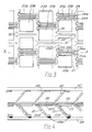
- Figure 1 is a schematic sectional view of part of the first device illustrating the surface of the pyroelectric layer carrying the discrete electrodes;
- Figure 2 shows an elevation view of a section at AA in Figure 1;
- Figure 3 is a schematic sectional view of part of the second device illustrating the surface of the pyroelectric layer carrying the discrete electrodes; and
- Figure 4 shows an elevation view of a section at AA in Figure 3.
- In the first device shown in Figures 1 and 2, a
pyroelectric film 21 of for example PVDF has a pattern of interconnectedgold electrodes 22 formed on one surface and a pattern ofdiscrete gold 23 formed on the other surface. Thefilm 21, interconnectedelectrodes 22 anddiscrete electrodes 23 together are effective to define an array of pyroelectric detector elements. On the surface of thefilm 21 between thediscrete electrodes 23, there is formed an intercalated pattern of electricallyconductive patches 24. Eachdiscrete electrode 23 is connected to arespective patch 24 by a long, narrowelectrical conductor 25, which passes between the adjacentdiscrete electrodes 23. Aslit 26 is cut in thefilm 21 around eachpatch 24 and along either side of therelevant conductor 25, thereby forming a tongue orstrip 27 of the film which is pulled out of the plane of the film. Eachpatch 24 at the end of arespective strip 27 is bonded to arespective input pad 28 of an integratedcircuit 29 arrangement whicn in use of the device performs signal processing of the electrical signals generated by the pyroelectric detector elements. Optionally, theslits 26 may be flared at the ends to widen the strip, as shown at 30, reducing the thermal conductance between adjacent pyroelectric elements on either side of theflared regions 30. Thefilm 21 and the integratedcircuit 29 are kept apart by suitable spacers (not shown in the Figures). - In the second device shown in Figures 3 and 4, corresponding features to those of the first device are correspondingly labelled. A
pyroelectric film 21 has a pattern of interconnectedelectrodes 22 formed on one side and a pattern of pairs ofdiscrete electrodes 23a, 23b and electricallyconductive patches 24a, 24b formed on the other side. Eachdiscrete electrodes 23a or 23b is connected to arespective patches 24a or 24b by a respectiveelectrical conductors adjacent electrodes 23a or 23b. The second device differs from the first device however in that aslit 26 is cut in the film around each pair ofpatches 24a, 24b and along either side of the relevant pair ofconductors strip 27 which is pulled out of the plane of the film. Eachpatch 24a or 24b is bonded to arespective input pads 28a or 28b of an integratedcircuit 29.Further slits 41 may be cut in thefilm 21 between adjacent pairs of discrete electrodes, the slits being U-shaped to formstrips 42 which are pulled out of the plane of the film and attached to atransparent cover plate 43 on the side of the film remote from the integratedcircuit 29. Theseslits 41 are flared at the ends adjacent to thediscrete electrodes 23a or 23b to widen the strip, as shown at 30, reducing the thermal conductance between adjacent pyroelectric detector elements on either side of theflared regions 30. Thefilm 21 is kept apart from the integratedcircuit 29 and from thecover glass 43 by suitable spacers (not shown in the Figures). The combination ofstrips 27 andstrips 42 are thus effective to maintain an equal spacing from thecover plate 43 and from the integratedcircuit 29 of each pyroelectric detector element. - The
inter-connected electrodes 22 are covered by an infrared absorbent layer (not shown), for example a layer of black gold. The inter-connections between these electrodes should be narrow, thin and preferably meandered to increase their length. They should also be connected to ground. - Clearly, embodiments of the present invention are not restricted to the particular shapes of electrodes shown and described herein before. Thus, the electrodes can be of a complex shape; in an advantageous form, the shape of the electrodes conforms to the isothermal-resistance contours of the device, such that the electrodes are located in regions wherein the thermal resistance to ground has a relatively high value (preferably being at its highest).
- It will be appreciated that whilst it is particularly convenient to form the pyroelectric layer from a flexible film of pyroelectric material, for example, a pyroelectric polymer, the invention is also applicable to devices in which the layer of pyroelectric material is a composite layer comprising an array of discrete regions of pyroelectric material carried on a flexible substrate, for example, of polyimide. The tongues will then be formed from regions of the flexible substrate, which do not necessarily carry pyroelectric regions.
Claims (9)
Priority Applications (1)
| Application Number | Priority Date | Filing Date | Title |
|---|---|---|---|
| AT89305499T ATE104472T1 (en) | 1988-06-01 | 1989-05-31 | DEVICE FOR TAKING THERMAL IMAGES. |
Applications Claiming Priority (2)
| Application Number | Priority Date | Filing Date | Title |
|---|---|---|---|
| GB8812958 | 1988-06-01 | ||
| GB888812958A GB8812958D0 (en) | 1988-06-01 | 1988-06-01 | Thermal imaging |
Publications (3)
| Publication Number | Publication Date |
|---|---|
| EP0345050A2 true EP0345050A2 (en) | 1989-12-06 |
| EP0345050A3 EP0345050A3 (en) | 1990-10-03 |
| EP0345050B1 EP0345050B1 (en) | 1994-04-13 |
Family
ID=10637884
Family Applications (1)
| Application Number | Title | Priority Date | Filing Date |
|---|---|---|---|
| EP89305499A Expired - Lifetime EP0345050B1 (en) | 1988-06-01 | 1989-05-31 | Thermal imaging device |
Country Status (7)
| Country | Link |
|---|---|
| US (1) | US4942301A (en) |
| EP (1) | EP0345050B1 (en) |
| JP (1) | JPH02236128A (en) |
| AT (1) | ATE104472T1 (en) |
| CA (1) | CA1323902C (en) |
| DE (1) | DE68914507T2 (en) |
| GB (1) | GB8812958D0 (en) |
Cited By (1)
| Publication number | Priority date | Publication date | Assignee | Title |
|---|---|---|---|---|
| EP0663696A2 (en) * | 1994-01-13 | 1995-07-19 | Texas Instruments Incorporated | Thermal imaging device |
Families Citing this family (3)
| Publication number | Priority date | Publication date | Assignee | Title |
|---|---|---|---|---|
| US5602391A (en) * | 1995-02-23 | 1997-02-11 | Hughes Electronics | Quincunx sampling grid for staring array |
| US5744801A (en) * | 1995-11-03 | 1998-04-28 | Servo Corporation Of America | Earth horizon sensor with staggered array of sensors |
| TW346688B (en) * | 1996-04-15 | 1998-12-01 | Matsushita Electric Works Ltd | Pyroelectric-type IR receiving element and IR sensor using the same |
Citations (2)
| Publication number | Priority date | Publication date | Assignee | Title |
|---|---|---|---|---|
| EP0173368A2 (en) * | 1984-08-24 | 1986-03-05 | Philips Electronics Uk Limited | A thermal imaging device and a method of manufacturing a thermal imaging device |
| EP0219555A1 (en) * | 1985-10-11 | 1987-04-29 | Sumitomo Bakelite Company Limited | Process for producing piezo-electric or pyro-electric composite sheet |
Family Cites Families (6)
| Publication number | Priority date | Publication date | Assignee | Title |
|---|---|---|---|---|
| US4060729A (en) * | 1976-12-10 | 1977-11-29 | Martin Marietta Corporation | Pyroelectric detector with decreased susceptibility to vibrational noise |
| US4214165A (en) * | 1979-02-21 | 1980-07-22 | Hughes Aircraft Company | Pyroelectric IR detector with signal capacitively coupled to an output circuit |
| GB2100058B (en) * | 1981-06-05 | 1985-03-20 | Philips Electronic Associated | Pyroelectric detector |
| US4660066A (en) * | 1982-09-08 | 1987-04-21 | Texas Instruments Incorporated | Structure for packaging focal plane imagers and signal processing circuits |
| US4532424A (en) * | 1983-04-25 | 1985-07-30 | Rockwell International Corporation | Pyroelectric thermal detector array |
| US4754139A (en) * | 1986-04-10 | 1988-06-28 | Aerojet-General Corporation | Uncooled high resolution infrared imaging plane |
-
1988
- 1988-06-01 GB GB888812958A patent/GB8812958D0/en active Pending
-
1989
- 1989-05-31 CA CA000601286A patent/CA1323902C/en not_active Expired - Fee Related
- 1989-05-31 EP EP89305499A patent/EP0345050B1/en not_active Expired - Lifetime
- 1989-05-31 DE DE68914507T patent/DE68914507T2/en not_active Expired - Fee Related
- 1989-05-31 AT AT89305499T patent/ATE104472T1/en not_active IP Right Cessation
- 1989-06-01 JP JP1137600A patent/JPH02236128A/en active Pending
- 1989-06-01 US US07/359,882 patent/US4942301A/en not_active Expired - Fee Related
Patent Citations (2)
| Publication number | Priority date | Publication date | Assignee | Title |
|---|---|---|---|---|
| EP0173368A2 (en) * | 1984-08-24 | 1986-03-05 | Philips Electronics Uk Limited | A thermal imaging device and a method of manufacturing a thermal imaging device |
| EP0219555A1 (en) * | 1985-10-11 | 1987-04-29 | Sumitomo Bakelite Company Limited | Process for producing piezo-electric or pyro-electric composite sheet |
Non-Patent Citations (1)
| Title |
|---|
| APPLIED PHYSICS LETTERS. vol. 39, no. 9, 01 November 1981, NEW YORK US pages 772 - 773; H.Yamazaki et al.: "Temperature dependence of the pyroelectric response of vinylidene fluoride trifluoroethylene copolymer and the effect of ..." * |
Cited By (2)
| Publication number | Priority date | Publication date | Assignee | Title |
|---|---|---|---|---|
| EP0663696A2 (en) * | 1994-01-13 | 1995-07-19 | Texas Instruments Incorporated | Thermal imaging device |
| EP0663696A3 (en) * | 1994-01-13 | 1995-08-16 | Texas Instruments Inc |
Also Published As
| Publication number | Publication date |
|---|---|
| ATE104472T1 (en) | 1994-04-15 |
| DE68914507T2 (en) | 1994-10-20 |
| US4942301A (en) | 1990-07-17 |
| GB8812958D0 (en) | 1988-10-05 |
| CA1323902C (en) | 1993-11-02 |
| JPH02236128A (en) | 1990-09-19 |
| DE68914507D1 (en) | 1994-05-19 |
| EP0345050A3 (en) | 1990-10-03 |
| EP0345050B1 (en) | 1994-04-13 |
Similar Documents
| Publication | Publication Date | Title |
|---|---|---|
| US6049080A (en) | Pyroelectric infrared sensor device | |
| KR0135119B1 (en) | Infrared detector | |
| JP4137196B2 (en) | Infrared detector and manufacturing method thereof | |
| US4110616A (en) | Pyroelectric detectors | |
| KR910003846A (en) | Polyimide Thermal Separation Mesa for Thermal Imaging Systems | |
| US3581092A (en) | Pyroelectric detector array | |
| US4575631A (en) | Infra-red detector | |
| SE8702531D0 (en) | THERMAL DETECTOR SETUP | |
| EP0345047B1 (en) | Thermal imaging device | |
| KR880013261A (en) | Photoreactive array | |
| US7232998B2 (en) | Bolometer-type infrared solid-state image sensor | |
| US4942301A (en) | Thermal imaging device | |
| GB2236900A (en) | Thermal-radiation detectors with polymer film element(s) | |
| EP0375205B1 (en) | Thermal imaging device | |
| US6114697A (en) | Bandgap radiation detector | |
| US20020131548A1 (en) | Detector for computer tomographs | |
| EP0414831B1 (en) | A dielectric bolometer | |
| EP3557203B1 (en) | Light detector | |
| US5130542A (en) | Thermal imaging devices | |
| EP0345049B1 (en) | Thermal imaging device | |
| JP2583615B2 (en) | Touch sensor | |
| AU596782B1 (en) | Imaging devices, elements and systems | |
| US5420420A (en) | Infrared detector | |
| EP1117978B1 (en) | Bolometer with a serpentine stress balancing member | |
| GB2200245A (en) | Thermal detector |
Legal Events
| Date | Code | Title | Description |
|---|---|---|---|
| PUAI | Public reference made under article 153(3) epc to a published international application that has entered the european phase |
Free format text: ORIGINAL CODE: 0009012 |
|
| AK | Designated contracting states |
Kind code of ref document: A2 Designated state(s): AT BE CH DE ES FR GB GR IT LI LU NL SE |
|
| PUAL | Search report despatched |
Free format text: ORIGINAL CODE: 0009013 |
|
| AK | Designated contracting states |
Kind code of ref document: A3 Designated state(s): AT BE CH DE ES FR GB GR IT LI LU NL SE |
|
| 17P | Request for examination filed |
Effective date: 19910221 |
|
| 17Q | First examination report despatched |
Effective date: 19930617 |
|
| GRAA | (expected) grant |
Free format text: ORIGINAL CODE: 0009210 |
|
| AK | Designated contracting states |
Kind code of ref document: B1 Designated state(s): AT BE CH DE ES FR GB GR IT LI LU NL SE |
|
| PG25 | Lapsed in a contracting state [announced via postgrant information from national office to epo] |
Ref country code: SE Free format text: THE PATENT HAS BEEN ANNULLED BY A DECISION OF A NATIONAL AUTHORITY Effective date: 19940413 Ref country code: NL Effective date: 19940413 Ref country code: LI Effective date: 19940413 Ref country code: GR Free format text: LAPSE BECAUSE OF FAILURE TO SUBMIT A TRANSLATION OF THE DESCRIPTION OR TO PAY THE FEE WITHIN THE PRESCRIBED TIME-LIMIT Effective date: 19940413 Ref country code: ES Free format text: THE PATENT HAS BEEN ANNULLED BY A DECISION OF A NATIONAL AUTHORITY Effective date: 19940413 Ref country code: CH Effective date: 19940413 Ref country code: BE Effective date: 19940413 Ref country code: AT Effective date: 19940413 |
|
| REF | Corresponds to: |
Ref document number: 104472 Country of ref document: AT Date of ref document: 19940415 Kind code of ref document: T |
|
| ITF | It: translation for a ep patent filed |
Owner name: FUMERO BREVETTI S.N.C. |
|
| REF | Corresponds to: |
Ref document number: 68914507 Country of ref document: DE Date of ref document: 19940519 |
|
| PG25 | Lapsed in a contracting state [announced via postgrant information from national office to epo] |
Ref country code: LU Free format text: LAPSE BECAUSE OF NON-PAYMENT OF DUE FEES Effective date: 19940531 |
|
| ET | Fr: translation filed | ||
| REG | Reference to a national code |
Ref country code: CH Ref legal event code: PL |
|
| NLV1 | Nl: lapsed or annulled due to failure to fulfill the requirements of art. 29p and 29m of the patents act | ||
| PLBE | No opposition filed within time limit |
Free format text: ORIGINAL CODE: 0009261 |
|
| STAA | Information on the status of an ep patent application or granted ep patent |
Free format text: STATUS: NO OPPOSITION FILED WITHIN TIME LIMIT |
|
| 26N | No opposition filed | ||
| REG | Reference to a national code |
Ref country code: FR Ref legal event code: TP |
|
| PGFP | Annual fee paid to national office [announced via postgrant information from national office to epo] |
Ref country code: DE Payment date: 19970606 Year of fee payment: 9 |
|
| PG25 | Lapsed in a contracting state [announced via postgrant information from national office to epo] |
Ref country code: DE Free format text: LAPSE BECAUSE OF NON-PAYMENT OF DUE FEES Effective date: 19990302 |
|
| PGFP | Annual fee paid to national office [announced via postgrant information from national office to epo] |
Ref country code: FR Payment date: 19990511 Year of fee payment: 11 |
|
| PGFP | Annual fee paid to national office [announced via postgrant information from national office to epo] |
Ref country code: GB Payment date: 19990526 Year of fee payment: 11 |
|
| PG25 | Lapsed in a contracting state [announced via postgrant information from national office to epo] |
Ref country code: GB Free format text: LAPSE BECAUSE OF NON-PAYMENT OF DUE FEES Effective date: 20000531 |
|
| GBPC | Gb: european patent ceased through non-payment of renewal fee |
Effective date: 20000531 |
|
| PG25 | Lapsed in a contracting state [announced via postgrant information from national office to epo] |
Ref country code: FR Free format text: LAPSE BECAUSE OF NON-PAYMENT OF DUE FEES Effective date: 20010131 |
|
| REG | Reference to a national code |
Ref country code: FR Ref legal event code: ST |
|
| PG25 | Lapsed in a contracting state [announced via postgrant information from national office to epo] |
Ref country code: IT Free format text: LAPSE BECAUSE OF NON-PAYMENT OF DUE FEES Effective date: 20050531 |