EP0344904A2 - Züchtung von halbisolierendem Indiumphosphid durch Epitaxie aus der Flüssigphase - Google Patents
Züchtung von halbisolierendem Indiumphosphid durch Epitaxie aus der Flüssigphase Download PDFInfo
- Publication number
- EP0344904A2 EP0344904A2 EP89303953A EP89303953A EP0344904A2 EP 0344904 A2 EP0344904 A2 EP 0344904A2 EP 89303953 A EP89303953 A EP 89303953A EP 89303953 A EP89303953 A EP 89303953A EP 0344904 A2 EP0344904 A2 EP 0344904A2
- Authority
- EP
- European Patent Office
- Prior art keywords
- inp
- concentration
- melt
- solution
- epitaxial layer
- Prior art date
- Legal status (The legal status is an assumption and is not a legal conclusion. Google has not performed a legal analysis and makes no representation as to the accuracy of the status listed.)
- Withdrawn
Links
- 238000004943 liquid phase epitaxy Methods 0.000 title claims abstract description 54
- GPXJNWSHGFTCBW-UHFFFAOYSA-N Indium phosphide Chemical compound [In]#P GPXJNWSHGFTCBW-UHFFFAOYSA-N 0.000 title 1
- 238000000034 method Methods 0.000 claims abstract description 49
- 239000000758 substrate Substances 0.000 claims abstract description 37
- 230000001590 oxidative effect Effects 0.000 claims abstract description 23
- 239000000356 contaminant Substances 0.000 claims abstract description 19
- 239000002019 doping agent Substances 0.000 claims abstract description 18
- OKTJSMMVPCPJKN-UHFFFAOYSA-N Carbon Chemical compound [C] OKTJSMMVPCPJKN-UHFFFAOYSA-N 0.000 claims description 19
- 229910002804 graphite Inorganic materials 0.000 claims description 19
- 239000010439 graphite Substances 0.000 claims description 19
- 239000004065 semiconductor Substances 0.000 claims description 10
- 229910052725 zinc Inorganic materials 0.000 claims description 10
- 238000004519 manufacturing process Methods 0.000 claims description 9
- 229910052793 cadmium Inorganic materials 0.000 claims description 5
- 238000001816 cooling Methods 0.000 claims description 5
- 239000012535 impurity Substances 0.000 claims description 4
- 229910052753 mercury Inorganic materials 0.000 claims description 4
- 229910052790 beryllium Inorganic materials 0.000 claims description 3
- 229910052749 magnesium Inorganic materials 0.000 claims description 3
- 238000002844 melting Methods 0.000 claims 13
- 230000008018 melting Effects 0.000 claims 13
- 238000005530 etching Methods 0.000 claims 5
- 229910052738 indium Inorganic materials 0.000 claims 3
- VYPSYNLAJGMNEJ-UHFFFAOYSA-N Silicium dioxide Chemical compound O=[Si]=O VYPSYNLAJGMNEJ-UHFFFAOYSA-N 0.000 description 47
- 235000012239 silicon dioxide Nutrition 0.000 description 44
- 239000010453 quartz Substances 0.000 description 41
- 239000013078 crystal Substances 0.000 description 21
- 239000007789 gas Substances 0.000 description 14
- 239000000155 melt Substances 0.000 description 14
- 239000000463 material Substances 0.000 description 10
- 239000000243 solution Substances 0.000 description 10
- OKKJLVBELUTLKV-UHFFFAOYSA-N Methanol Chemical compound OC OKKJLVBELUTLKV-UHFFFAOYSA-N 0.000 description 9
- VNWKTOKETHGBQD-UHFFFAOYSA-N methane Natural products C VNWKTOKETHGBQD-UHFFFAOYSA-N 0.000 description 9
- 239000012153 distilled water Substances 0.000 description 6
- 150000002500 ions Chemical class 0.000 description 6
- XLYOFNOQVPJJNP-UHFFFAOYSA-N water Chemical compound O XLYOFNOQVPJJNP-UHFFFAOYSA-N 0.000 description 6
- 239000002244 precipitate Substances 0.000 description 5
- 238000002488 metal-organic chemical vapour deposition Methods 0.000 description 4
- GRYLNZFGIOXLOG-UHFFFAOYSA-N Nitric acid Chemical compound O[N+]([O-])=O GRYLNZFGIOXLOG-UHFFFAOYSA-N 0.000 description 3
- 230000015572 biosynthetic process Effects 0.000 description 3
- 229910052681 coesite Inorganic materials 0.000 description 3
- 229910052906 cristobalite Inorganic materials 0.000 description 3
- 238000001035 drying Methods 0.000 description 3
- 238000010438 heat treatment Methods 0.000 description 3
- 238000003780 insertion Methods 0.000 description 3
- 230000037431 insertion Effects 0.000 description 3
- 229910017604 nitric acid Inorganic materials 0.000 description 3
- 238000010926 purge Methods 0.000 description 3
- 239000000377 silicon dioxide Substances 0.000 description 3
- 239000007787 solid Substances 0.000 description 3
- 229910052682 stishovite Inorganic materials 0.000 description 3
- 229910052905 tridymite Inorganic materials 0.000 description 3
- 229910017401 Au—Ge Inorganic materials 0.000 description 2
- 238000003486 chemical etching Methods 0.000 description 2
- 238000011109 contamination Methods 0.000 description 2
- 238000005259 measurement Methods 0.000 description 2
- 230000003647 oxidation Effects 0.000 description 2
- 238000007254 oxidation reaction Methods 0.000 description 2
- 239000007858 starting material Substances 0.000 description 2
- 230000005355 Hall effect Effects 0.000 description 1
- 229910018104 Ni-P Inorganic materials 0.000 description 1
- 229910018536 Ni—P Inorganic materials 0.000 description 1
- 229910009973 Ti2O3 Inorganic materials 0.000 description 1
- 229910001297 Zn alloy Inorganic materials 0.000 description 1
- 239000000969 carrier Substances 0.000 description 1
- 230000015556 catabolic process Effects 0.000 description 1
- 239000004020 conductor Substances 0.000 description 1
- 238000006731 degradation reaction Methods 0.000 description 1
- 238000000151 deposition Methods 0.000 description 1
- 230000008021 deposition Effects 0.000 description 1
- 238000002347 injection Methods 0.000 description 1
- 239000007924 injection Substances 0.000 description 1
- 239000011810 insulating material Substances 0.000 description 1
- 239000012212 insulator Substances 0.000 description 1
- 239000007788 liquid Substances 0.000 description 1
- 230000007774 longterm Effects 0.000 description 1
- 230000000873 masking effect Effects 0.000 description 1
- 229910044991 metal oxide Inorganic materials 0.000 description 1
- 238000001451 molecular beam epitaxy Methods 0.000 description 1
- 238000012544 monitoring process Methods 0.000 description 1
- 230000003287 optical effect Effects 0.000 description 1
- 238000012545 processing Methods 0.000 description 1
- 230000006798 recombination Effects 0.000 description 1
- 238000005215 recombination Methods 0.000 description 1
- 238000007790 scraping Methods 0.000 description 1
- 238000007789 sealing Methods 0.000 description 1
- 230000035945 sensitivity Effects 0.000 description 1
- GQUJEMVIKWQAEH-UHFFFAOYSA-N titanium(III) oxide Chemical compound O=[Ti]O[Ti]=O GQUJEMVIKWQAEH-UHFFFAOYSA-N 0.000 description 1
- 230000001988 toxicity Effects 0.000 description 1
- 231100000419 toxicity Toxicity 0.000 description 1
Images

Classifications
-
- C—CHEMISTRY; METALLURGY
- C30—CRYSTAL GROWTH
- C30B—SINGLE-CRYSTAL GROWTH; UNIDIRECTIONAL SOLIDIFICATION OF EUTECTIC MATERIAL OR UNIDIRECTIONAL DEMIXING OF EUTECTOID MATERIAL; REFINING BY ZONE-MELTING OF MATERIAL; PRODUCTION OF A HOMOGENEOUS POLYCRYSTALLINE MATERIAL WITH DEFINED STRUCTURE; SINGLE CRYSTALS OR HOMOGENEOUS POLYCRYSTALLINE MATERIAL WITH DEFINED STRUCTURE; AFTER-TREATMENT OF SINGLE CRYSTALS OR A HOMOGENEOUS POLYCRYSTALLINE MATERIAL WITH DEFINED STRUCTURE; APPARATUS THEREFOR
- C30B19/00—Liquid-phase epitaxial-layer growth
- C30B19/02—Liquid-phase epitaxial-layer growth using molten solvents, e.g. flux
- C30B19/04—Liquid-phase epitaxial-layer growth using molten solvents, e.g. flux the solvent being a component of the crystal composition
-
- C—CHEMISTRY; METALLURGY
- C30—CRYSTAL GROWTH
- C30B—SINGLE-CRYSTAL GROWTH; UNIDIRECTIONAL SOLIDIFICATION OF EUTECTIC MATERIAL OR UNIDIRECTIONAL DEMIXING OF EUTECTOID MATERIAL; REFINING BY ZONE-MELTING OF MATERIAL; PRODUCTION OF A HOMOGENEOUS POLYCRYSTALLINE MATERIAL WITH DEFINED STRUCTURE; SINGLE CRYSTALS OR HOMOGENEOUS POLYCRYSTALLINE MATERIAL WITH DEFINED STRUCTURE; AFTER-TREATMENT OF SINGLE CRYSTALS OR A HOMOGENEOUS POLYCRYSTALLINE MATERIAL WITH DEFINED STRUCTURE; APPARATUS THEREFOR
- C30B29/00—Single crystals or homogeneous polycrystalline material with defined structure characterised by the material or by their shape
- C30B29/10—Inorganic compounds or compositions
- C30B29/40—AIIIBV compounds wherein A is B, Al, Ga, In or Tl and B is N, P, As, Sb or Bi
-
- H—ELECTRICITY
- H01—ELECTRIC ELEMENTS
- H01L—SEMICONDUCTOR DEVICES NOT COVERED BY CLASS H10
- H01L21/00—Processes or apparatus adapted for the manufacture or treatment of semiconductor or solid state devices or of parts thereof
- H01L21/02—Manufacture or treatment of semiconductor devices or of parts thereof
- H01L21/02104—Forming layers
- H01L21/02365—Forming inorganic semiconducting materials on a substrate
- H01L21/02367—Substrates
- H01L21/0237—Materials
- H01L21/02387—Group 13/15 materials
- H01L21/02392—Phosphides
-
- H—ELECTRICITY
- H01—ELECTRIC ELEMENTS
- H01L—SEMICONDUCTOR DEVICES NOT COVERED BY CLASS H10
- H01L21/00—Processes or apparatus adapted for the manufacture or treatment of semiconductor or solid state devices or of parts thereof
- H01L21/02—Manufacture or treatment of semiconductor devices or of parts thereof
- H01L21/02104—Forming layers
- H01L21/02365—Forming inorganic semiconducting materials on a substrate
- H01L21/02436—Intermediate layers between substrates and deposited layers
- H01L21/02439—Materials
- H01L21/02455—Group 13/15 materials
- H01L21/02461—Phosphides
-
- H—ELECTRICITY
- H01—ELECTRIC ELEMENTS
- H01L—SEMICONDUCTOR DEVICES NOT COVERED BY CLASS H10
- H01L21/00—Processes or apparatus adapted for the manufacture or treatment of semiconductor or solid state devices or of parts thereof
- H01L21/02—Manufacture or treatment of semiconductor devices or of parts thereof
- H01L21/02104—Forming layers
- H01L21/02365—Forming inorganic semiconducting materials on a substrate
- H01L21/02518—Deposited layers
- H01L21/02521—Materials
- H01L21/02538—Group 13/15 materials
- H01L21/02543—Phosphides
-
- H—ELECTRICITY
- H01—ELECTRIC ELEMENTS
- H01L—SEMICONDUCTOR DEVICES NOT COVERED BY CLASS H10
- H01L21/00—Processes or apparatus adapted for the manufacture or treatment of semiconductor or solid state devices or of parts thereof
- H01L21/02—Manufacture or treatment of semiconductor devices or of parts thereof
- H01L21/02104—Forming layers
- H01L21/02365—Forming inorganic semiconducting materials on a substrate
- H01L21/02518—Deposited layers
- H01L21/0257—Doping during depositing
- H01L21/02573—Conductivity type
- H01L21/02579—P-type
-
- H—ELECTRICITY
- H01—ELECTRIC ELEMENTS
- H01L—SEMICONDUCTOR DEVICES NOT COVERED BY CLASS H10
- H01L21/00—Processes or apparatus adapted for the manufacture or treatment of semiconductor or solid state devices or of parts thereof
- H01L21/02—Manufacture or treatment of semiconductor devices or of parts thereof
- H01L21/02104—Forming layers
- H01L21/02365—Forming inorganic semiconducting materials on a substrate
- H01L21/02518—Deposited layers
- H01L21/0257—Doping during depositing
- H01L21/02573—Conductivity type
- H01L21/02581—Transition metal or rare earth elements
-
- H—ELECTRICITY
- H01—ELECTRIC ELEMENTS
- H01L—SEMICONDUCTOR DEVICES NOT COVERED BY CLASS H10
- H01L21/00—Processes or apparatus adapted for the manufacture or treatment of semiconductor or solid state devices or of parts thereof
- H01L21/02—Manufacture or treatment of semiconductor devices or of parts thereof
- H01L21/02104—Forming layers
- H01L21/02365—Forming inorganic semiconducting materials on a substrate
- H01L21/02612—Formation types
- H01L21/02617—Deposition types
- H01L21/02623—Liquid deposition
- H01L21/02625—Liquid deposition using melted materials
-
- H—ELECTRICITY
- H01—ELECTRIC ELEMENTS
- H01L—SEMICONDUCTOR DEVICES NOT COVERED BY CLASS H10
- H01L21/00—Processes or apparatus adapted for the manufacture or treatment of semiconductor or solid state devices or of parts thereof
- H01L21/02—Manufacture or treatment of semiconductor devices or of parts thereof
- H01L21/02104—Forming layers
- H01L21/02365—Forming inorganic semiconducting materials on a substrate
- H01L21/02612—Formation types
- H01L21/02617—Deposition types
- H01L21/02623—Liquid deposition
- H01L21/02628—Liquid deposition using solutions
-
- H—ELECTRICITY
- H01—ELECTRIC ELEMENTS
- H01L—SEMICONDUCTOR DEVICES NOT COVERED BY CLASS H10
- H01L21/00—Processes or apparatus adapted for the manufacture or treatment of semiconductor or solid state devices or of parts thereof
- H01L21/02—Manufacture or treatment of semiconductor devices or of parts thereof
- H01L21/02104—Forming layers
- H01L21/02365—Forming inorganic semiconducting materials on a substrate
- H01L21/02612—Formation types
- H01L21/02617—Deposition types
- H01L21/02636—Selective deposition, e.g. simultaneous growth of mono- and non-monocrystalline semiconductor materials
- H01L21/02639—Preparation of substrate for selective deposition
-
- H—ELECTRICITY
- H01—ELECTRIC ELEMENTS
- H01L—SEMICONDUCTOR DEVICES NOT COVERED BY CLASS H10
- H01L21/00—Processes or apparatus adapted for the manufacture or treatment of semiconductor or solid state devices or of parts thereof
- H01L21/67—Apparatus specially adapted for handling semiconductor or electric solid state devices during manufacture or treatment thereof; Apparatus specially adapted for handling wafers during manufacture or treatment of semiconductor or electric solid state devices or components ; Apparatus not specifically provided for elsewhere
- H01L21/67005—Apparatus not specifically provided for elsewhere
- H01L21/67011—Apparatus for manufacture or treatment
- H01L21/67098—Apparatus for thermal treatment
- H01L21/67115—Apparatus for thermal treatment mainly by radiation
-
- H—ELECTRICITY
- H10—SEMICONDUCTOR DEVICES; ELECTRIC SOLID-STATE DEVICES NOT OTHERWISE PROVIDED FOR
- H10H—INORGANIC LIGHT-EMITTING SEMICONDUCTOR DEVICES HAVING POTENTIAL BARRIERS
- H10H20/00—Individual inorganic light-emitting semiconductor devices having potential barriers, e.g. light-emitting diodes [LED]
- H10H20/80—Constructional details
- H10H20/81—Bodies
- H10H20/811—Bodies having quantum effect structures or superlattices, e.g. tunnel junctions
-
- H—ELECTRICITY
- H10—SEMICONDUCTOR DEVICES; ELECTRIC SOLID-STATE DEVICES NOT OTHERWISE PROVIDED FOR
- H10H—INORGANIC LIGHT-EMITTING SEMICONDUCTOR DEVICES HAVING POTENTIAL BARRIERS
- H10H20/00—Individual inorganic light-emitting semiconductor devices having potential barriers, e.g. light-emitting diodes [LED]
- H10H20/80—Constructional details
- H10H20/81—Bodies
- H10H20/822—Materials of the light-emitting regions
- H10H20/824—Materials of the light-emitting regions comprising only Group III-V materials, e.g. GaP
Definitions
- This invention relates to the growth of semi-insulating InP by Liquid Phase Epitaxy (LPE).
- LPE Liquid Phase Epitaxy
- a series of doped epitaxial layers are grown on a semiconductor substrate to define a heterostructure. Regions of the epitaxial layers are etched back to define an isolated mesa in the heterostructure which functions as an active region of the completed laser. The etched regions are covered with isolating material to planarize the structure, and contacts are formed to the active region and to the substrate. End facets are cleaved on the active region to complete the laser fabrication.
- the isolating material used to planarize the structure must be compatible with the crystal structure of the heterostructure to avoid mechanical stresses leading to reliability problems and to avoid the formation of surface states which could act as recombination centers reducing the efficiency of the completed laser.
- the isolating material must also have a refractive index lower than that of the active region of the heterostructure so that the active region acts as an optical waveguide.
- the isolating material must be a relatively poor conductor since current flow through the isolating material to the substrate would limit the flow of injection current through the active region of the heterostructure.
- the process used to cover the etched regions with isolating material must also be compatible with the crystal structure of the heterostructure to avoid degradation of the heterostructure during planarization.
- Dutta et al have filled channels isolating a InP-InGaAsP buried heterostructure laser by masking regions adjacent the channels with a layer of SiO2, and selectively growing Fe-doped InP in the exposed channels using metalorganic vapour phase epitaxy (MOVPE) growth processes (Appl. Phys. Lett. 48 (23), pp. 1572-1573, 9 June 1986; Appl. Phys. Lett. 50 (11), pp. 644-646, 16 March 1987).
- MOVPE metalorganic vapour phase epitaxy
- the Fe-doped InP acts as a semi-insulator to inhibit flow of current through the filled channels, and has the required refractive index and crystal compatibility properties.
- MOVPE-grown Fe-doped InP contains Fe-P precipitates which may degrade the long term reliability of such lasers (J. Crystal Growth 72 . p.693, 1985).
- MOVPE growth processes tend to produce a nonplanar epitaxial layer.
- Lambert et al reported growth of Ti-Hg co-doped semi-insulating InP ingots by a gradient freeze method (Semicond. Sci. Technol. 2 (1987), pp.78-82).
- the gradient freeze method is used to grow crystal ingots and is not applicable to the selective epitaxial growth of crystal layers on a substrate since the high melt temperatures used would decompose the substrate.
- Iseler et al reported growth of Ti-Zn, Ti-Cd and Ti-Be codoped semi-insulating InP boules by the Liquid Encapsulated Czochralski (LEC) method (Appl. Phys. Lett. 48 (24), pp.1656-1657, June 16, 1986).
- the LEC method also is not applicable to the selective epitaxial growth of crystal layers on a substrate since the high melt temperatures used would decompose the substrate.
- the present invention seeks to provide a method for Liquid Phase Epitaxy (LPE) of semi-insulating InP applicable to the selective growth of isolating material on a substrate to isolate the active region of a buried heterostructure semiconductor laser.
- LPE Liquid Phase Epitaxy
- the present invention seeks to provide a method for Liquid Phase Epitaxy (LPE) of semi-insulating InP which is practicable at a temperature below 650 degrees Celsius and which forms fewer unwanted precipitates than known methods for epitaxial growth of semi-insulating InP.
- LPE Liquid Phase Epitaxy
- One aspect of the invention provides a method for Liquid Phase Epitaxy (LPE) of semi-insulating InP, the method comprising cooling a solution of P, Ti and a p-type dopant in molten In in a non-oxidizing ambient at a surface of a substrate to grow an epitaxial layer of doped InP on said surface, the concentration of p-type dopant in said solution being such as to provide a concentration of p-type dopant in the grown epitaxial layer greater than the aggregate concentration of any residual contaminants in the grown epitaxial layer, and the concentration of Ti in said solution being such as to provide a concentration of Ti in the grown epitaxial layer greater than the concentration of p-type dopant in the grown epitaxial layer.
- LPE Liquid Phase Epitaxy
- the p-type dopant may be selected from the group consisting of Zn, Cd, Hg, Be and Mg, and is preferably Zn.
- a preferred embodiment of the invention provides a method for Liquid Phase Epitaxy (LPE) of semi-insulating InP, comprising cooling a solution of P, Ti and Zn in molten In in a non-oxidizing ambient at a surface of a substrate to grow an epitaxial layer of doped InP on said surface, the concentration of Zn in said solution being such as to provide a concentration of Zn in the grown epitaxial layer greater than the aggregate concentration of any residual contaminants in the grown epitaxial layer, and the concentration of Ti in said solution being such as to provide a concentration of Ti in the grown epitaxial layer greater than the concentration of Zn in the grown epitaxial layer.
- LPE Liquid Phase Epitaxy
- the LPE method of the preferred embodiment is practicable at temperatures below 650 degrees Celsius and forms fewer unwanted precipitates than previously reported methods for LPE of semi-insulating InP.
- the LPE method of the preferred embodiment is easier to control than MOVPE methods, and is compatible with selective epitaxial growth of semi-insulating InP to isolate an active region of a buried heterostructure semiconductor laser unlike previously reported gradient freeze and LEC methods for growth of semi-insulating InP ingots and boules.
- another aspect of the invention provides a method of making a buried heterostructure semiconductor laser, comprising: growing an InP-InGaAsP heterostructure on an InP substrate; removing regions of the heterostructure to define a mesa; growing a layer of semi-insulating InP adjacent the mesa by LPE to electrically isolate the mesa; forming electrical contacts to the mesa and to the substrate; and forming reflective end facets on the mesa.
- a layer of Ti-Zn codoped semi-insulating InP is grown in the channels by LPE at temperatures below 650 degrees Celsius.
- yet another aspect of the invention provides a buried heterostructure semiconductor laser, comprising: an InP substrate; a series of epitaxial layers on said substrate defining a heterostructure having reflective end facets; a layer of Ti-Zn codoped semi-insulating InP adjacent the heterostructure electrically isolating said heterostructure; and electrical contacts to the isolated region of the heterostructure and to the substrate.
- an n-type InP epitaxial layer 12 In the fabrication of a buried heterostructure semiconductor laser, an n-type InP epitaxial layer 12, an n-type InGaAsP epitaxial layer 14, a p-type InP epitaxial layer 16 and a p-type InGaAsP epitaxial layer 18 are successively grown on an n-type InP substrate 10 to define a heterostructure as shown in Figure 1a.
- the epitaxial layers may be grown by Liquid Phase Epitaxy (LPE), Metalorganic Vapour Phase Epitaxy (MOVPE), Molecular Beam Epitaxy (MBE) or any other suitable epitaxial growth technique.
- LPE Liquid Phase Epitaxy
- MOVPE Metalorganic Vapour Phase Epitaxy
- MBE Molecular Beam Epitaxy
- a surface region of the p-type InGaAsP epitaxial layer 18 is masked and adjacent regions of the epitaxial layers 12, 14, 16, 18 are removed by chemical etching to define a mesa 20, as shown in Figure 1b.
- a layer 30 of Ti-Zn codoped semi-insulating InP is selectively grown adjacent the mesa, as shown in Figure 1c, by a Liquid Phase Epitaxy (LPE) process described below.
- LPE Liquid Phase Epitaxy
- the LPE process is carried out at temperatures below 650 degrees Celsius to avoid damage to the other epitaxial layers 12, 14, 16, 18 defining the heterostructure.
- a SiO2 mask 22 may be used to prevent growth of the layer 30 on the mesa 20.
- the layer 30 is grown to substantially the same height as the mesa 20 to planarize the structure.
- the semi-insulating material of the layer 30 electrically isolates the mesa 20.
- a SiO2 dielectric layer 40 is formed on the upper surface of the resulting structure, a contact hole is opened through the dielectric layer 40 over the mesa 20, and an Au-Zn layer 50 is deposited over the contact hole to form an electrical contact to the mesa 20, as shown in Figure 1d.
- the p-type InGaAsP layer 18 permits formation of an ohmic contact to the underlying p-type InP layer 16.
- An Au-Ge layer 60 is deposited on the back surface of the substrate 10 to form an electrical contact to the substrate 10, as shown in Figure 1d. Material may be removed from the back of the substrate 10 before deposition of the Au-Ge layer 60 to reduce the series resistance of the resulting laser. Reflective end facets are cleaved to complete the laser fabrication.
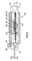
- the LPE growth of the Ti-Zn codoped semi-insulating InP layer 30 is carried out in apparatus 100 shown schematically in Figure 2.
- the apparatus 100 comprises a quartz tube 110 which is sealed at one end 112 and open at another end 114.
- the tube 110 is provided with a gas inlet 116 and a gas outlet 118, and a removable cover (not shown) for sealing the open end 114.
- a source of Pd purified H2 (not shown) is connected to the gas inlet 116 to maintain a non-oxidizing ambient in the tube 110.
- the tube 110 is surrounded by a heating element 120 connected to a temperature monitoring and control system (not shown) which permits precise control of the temperature within the tube 110.
- the tube 110 carries a graphite boat 130 having a plurality of compartments 132 for containing growth melts 140.
- Each of the compartments 132 has a bottom opening 133 which communicates with a slider channel 135 extending along the boat 130.
- the slider channel 135 slidably receives a graphite slider 137 which includes a wafer recess 138 for carrying a crystal wafer 150. Sliding movement of the slider 137 along the slider channel 135 aligns the wafer recess 138 successively with the bottom openings 133 of each compartment 132 to bring the crystal wafer 150 into successive contact with each of the growth melts 140.
- a loading device 160 in the form of a quartz rod 162 having a hollow recess 164 at one end is provided for loading compartments 132 without removing the boat 130 from the tube 110.
- a solid sample of In of 6N+ purity is etched in 50% distilled water and 50% HNO3 for 5 minutes to remove surface oxides and other surface contaminants.
- the etched In sample is then rinsed with distilled water, rinsed with CH3OH and dried in a N2 cabinet.
- the In sample is inserted into a compartment 132 of the graphite boat 130, and the graphite boat 130 is inserted into the quartz tube 110.
- Pd purified H2 is supplied to the quartz tube 110 via the gas inlet 116 for 1.5 hours to purge the quartz tube 110 of oxidizing gases.
- the temperature of the quartz tube 110 is then raised to 700 degrees Celsius to melt In sample in a Pd purified H2 ambient.
- the resulting In melt is baked at 700 degrees Celsius in a Pd purified H2 ambient for 20 hours to drive impurities from the In melt and cooled to room temperature to resolidify the In.
- a piece of Zn-doped InP having a carrier concentration of approximately 5x1018 cm ⁇ 3 and a piece of undoped InP are each etched in 2% Br2:CH3OH to remove surface oxides and other surface contaminants, rinsed in CH3OH and dried in a N2 cabinet.
- a piece of Ti wire of 4N purity is scraped with a surgical blade to remove surface oxides.
- the quartz tube 110 is purged with high purity N2 gas, and the etched InP and the deoxidized Ti wire are immediately added to the compartment 132 containing the In without removing the graphite boat 130 from the quartz tube 110.
- the quartz rod 162 is used to place the etched InP and deoxidized Ti in the compartment 132.
- a crystal wafer 150 is inserted into the wafer recess 138 of the slider 137.
- the crystal wafer 150 comprises an InP substrate 10 carrying epitaxial layers 12, 14, 16, 18 defining a heterostructure mesa 20 as shown in Figure 1b.
- the high purity N2 gas flow is maintained during the addition of the InP and Ti wire, and during the insertion of the crystal wafer to maintain the non-oxidizing ambient in the quartz tube 110.
- the quartz tube 110 is purged with Pd purified H2 for 1.5 hours.
- the temperature of the quartz tube 110 is then raised to 660 degrees Celsius for one hour to melt the In, InP and Ti.
- the Pd purified H2 gas flow is maintained during heating of the resulting melt to maintain the non-oxidizing ambient in the quartz tube 110.
- the resulting melt comprises a solution of P, Ti and Zn in molten In.
- the weight and carrier concentration of the Zn-doped substrate, the weight of the undoped InP substrate and the weight of the Ti wire are selected to provide a Zn concentration of 6x10 ⁇ 7 moles of Zn per mole of In, a Ti concentration of 1.2x10 ⁇ 4 moles of Ti per mole of In and a P concentration of 6.54x10 ⁇ 3 moles of P per mole of In in the solution.
- the temperature of the quartz tube 110 is then reduced to 635.5 degrees Celsius, and the slider 137 is advanced along the slider channel 135 to bring the crystal wafer 150 into contact with the melt.
- the temperature of the quartz tube 110 is further lowered at 0.12 degrees Celsius per minute to cause selective LPE growth of Ti-Zn codoped InP layers adjacent the mesa 20 on the substrate 10.
- the LPE growth is continued until the Ti-Zn codoped InP is grown to substantially the same height as the mesa 20.
- the slider 137 carrying the crystal wafer 150 is then withdrawn to separate the crystal wafer 150 from the growth melt, and the remaining laser fabrication steps are performed as described above.
- a solid sample of In of 6N+ purity is etched in 50% distilled water and 50% HNO3 for 5 minutes to remove surface oxides and other surface contaminants.
- the etched In sample is then rinsed with distilled water, rinsed with CH3OH and dried in a N2 cabinet.
- the In sample is inserted into a compartment 132 of the graphite boat 130, and the graphite boat 130 is inserted into the quartz tube 110.
- Pd purified H2 is supplied to the quartz tube 110 via the gas inlet 116 for 1.5 hours to purge the quartz tube 110 of oxidizing gases.
- the temperature of the quartz tube 110 is then raised to 700 degrees Celsius to melt the In sample in a Pd purified H2 ambient.
- the resulting In melt is baked at 700 degrees Celsius in a Pd purified H2 ambient for 20 hours to drive impurities from the In melt.
- the quartz tube 110 is then cooled to room temperature to resolidify the In.
- a piece of Ti wire of 4N purity is scraped with a surgical blade to remove surface oxides and a piece of undoped InP is etched in 2% Br2:CH3OH to remove surface oxides and other surface contaminants, rinsed in CH3OH and dried in a N2 cabinet.
- the quartz tube 110 is purged with high purity N2 and the etched InP and the deoxidized Ti wire are immediately added to the In in the compartment 132 without removing the graphite boat 130 from the quartz tube 110.
- the quartz rod 162 is used to place the InP and Ti in the compartment 132.
- the high purity N2 flow is maintained during addition of the Inp and Ti wire to maintain the non-oxidizing ambient in the quartz tube 110.
- the quartz tube 110 is purged with Pd purified H2 for 1.5 hours.
- the temperature of the quartz tube 110 is then raised to 660 degrees Celsius to melt the In, InP and Ti, and the resulting melt is maintained at 660 degrees Celsius for 5 hours to dissolve the added InP and Ti in the In, and to drive some of the dissolved Ti into walls of the compartment 132.
- the Pd purified H2 flow is maintained during baking to maintain the non-oxidizing ambient in the quartz tube 110.
- the weight of the Ti wire is selected to provide a Ti concentration of 7.2x10 ⁇ 4 moles of Ti per mole of In, and the weight of the InP is selected to provide a P concentration of 6.54x10 ⁇ 3 moles of P per mole of In in the melt.
- the melt is removed from the graphite boat 130, leaving Ti in the walls of the compartment 132 which contained the melt.
- Another solid sample of In of 6N+ purity is etched in 50% distilled water and 50% HNO3 for 5 minutes to remove surface oxides and other surface contaminants.
- the etched In sample is then rinsed with distilled water, rinsed with CH3OH and dried in a N2 cabinet.
- the In sample is inserted into the same compartment 132 of the graphite boat 130 used for the previous melt, and the graphite boat 130 is inserted into the quartz tube 110.
- Pd purified H2 is supplied to the quartz tube 110 via the gas inlet 116 for 1.5 hours to purge the quartz tube 110 of oxidizing gases.
- the temperature of the quartz tube 110 is then raised to 700 degrees Celsius to melt the In sample in a Pd purified H2 ambient.
- the resulting In melt is baked at 700 degrees Celsius in a Pd purified H2 ambient for 20 hours to drive impurities from the In melt and to draw Ti from the walls of the compartment 132 into the melt.
- the quartz tube 110 is then cooled to room temperature to resolidify the melt.
- a piece of Zn-doped InP having a carrier concentration of approximately 5x1018 cm ⁇ 3 and a piece of undoped InP are each etched in 2% Br2:CH3OH to remove surface oxides and other surface contaminants, rinsed in CH3OH and dried in a N2 cabinet.
- the quartz tube 110 is purged with high purity N2 and the etched InP pieces are immediately added to the compartment 132 containing the resolidified melt without removing the graphite boat 130 from the quartz tube 110.
- the quartz rod 162 is used to place the InP pieces in the compartment 132.
- a crystal wafer 150 is then inserted into the wafer recess 138 of the slider 137.
- the crystal wafer 150 comprises an InP substrate 10 carrying epitaxial layers 12, 14, 16, 18 defining a heterostructure mesa 20 as shown in Figure 1b.
- the high purity N2 gas flow is maintained during the addition of the InP pieces and during the insertion of the crystal wafer 150 to maintain the non-oxidizing ambient in the quartz tube 110.
- the quartz tube 110 is purged with Pd purified H2 for 1.5 hours.
- the temperature of the quartz tube 110 is then raised to 660 degrees Celsius to melt the resolidified melt and the added InP, and the resulting melt is maintained at 660 degrees Celsius for one hour to dissolve the added InP in the resulting melt.
- the Pd purified H2 gas flow is maintained during heating of the resulting melt to maintain the non-oxidizing ambient in the quartz tube 110.
- the resulting melt comprises a solution of P, Ti and Zn in molten In.
- the weight and carrier concentration of the Zn-doped substrate and the weight of the undoped InP substrate are selected to provide a Zn concentration of 6x10 ⁇ 7 moles of Zn per mole of In and a P concentration of 6.54x10 ⁇ 3 moles of P per mole of In in the solution.
- the weight of the Ti wire used in the previous melt and the baking time and temperature of the previous melt are selected to provide a Ti concentration of approximately 1.2x10 ⁇ 4 moles of Ti per mole of In in the second melt.
- the temperature of the quartz tube 110 is then reduced to 635.5 degrees Celsius, and the slider 137 is advanced along the slider channel 135 to bring the crystal wafer 150 into contact with the melt.
- the temperature of the quartz tube 110 is further lowered at 0.12 degrees Celsius per minute to cause selective LPE growth of Ti-Zn codoped InP layers adjacent the mesa 20 on the substrate 10.
- the LPE growth is continued until the Ti-Zn codoped InP is grown to substantially the same height as the mesa 20.
- the slider 137 carrying the crystal wafer 150 is then withdrawn to separate the crystal wafer 150 from the growth melt, and the remaining laser fabrication steps are performed as described above.
- the Ti-Zn codoped InP layer 30 grown by the LPE processes described above is a semi-insulating layer effective for electrically isolating the mesa 20.
- Zn ions in the Ti-Zn codoped InP accept conduction band electrons contributed by predominantly n-type residual contaminants in the InP.
- the Zn concentration in the grown epitaxial layer 30 is greater than the concentration of residual contaminants in the grown epitaxial layer 30, so the Zn ions contribute a net concentration of valence band holes.
- the Ti ions contribute electrons which fill the remaining valence band holes provided by the Zn ions.
- the Ti concentration in the grown epitaxial layer 30 is greater than the Zn concentration in the grown epitaxial layer 30, so that electrons contributed by the Ti ions fill essentially all of the remaining valence band holes provided by the Zn ions.
- the Ti energy levels are sufficiently far from the conduction and valence band edges in InP that excess Ti atoms contribute very few mobile electrons to the conduction band.
- the scarcity of mobile carriers accounts for the semi-insulating properties of the LPE grown Ti-Zn codoped InP layer 30.
- the concentrations of Zn used in the growth melt must be selected so as to ensure that the concentration of Zn in the grown epitaxial layer is greater than the aggregate concentration of any residual contaminants in the grown epitaxial layer, and the concentration of Ti used in the growth melt must be selected so as to ensure that the concentration of Ti in the grown epitaxial layer is greater than the concentration of Zn in the grown epitaxial layer.
- Suitable growth melt concentrations can be determined empirically by growth of sample crystals.
- InP layers can be grown by LPE from melts having increasing Zn concentrations until Hall Effect measurements indicate that p-type InP has been obtained in order to determine the growth melt concentration of Zn required to provide an epitaxial layer having a Zn concentration which exceeds the aggregate concentration of residual n-type contaminants.
- InP layers can then be grown by LPE from melts having the determined Zn concentration and increasing Ti concentrations until conductivity measurements indicate that semi-insulating InP has been obtained in order to determine the growth melt concentration of Ti required to an epitaxial layer having a Ti concentration which exceeds the Zn concentration.
- the required melt concentrations may vary if starting materials or growth conditions are altered.
- the Zn concentration in the melt must be at least 4x10 ⁇ 7 moles of Zn per mole of In and the Ti concentration must be at least 200 times the concentration of Zn in the melt.
- Zn is preferred because of its relatively low vapour pressure in the LPE growth melt at temperatures around 650 degrees Celsius and its limited tendency to migrate in InP at the temperatures used for epitaxial growth and subsequent processing.
- the relatively high vapour pressures for Cd and Hg in the LPE growth melt, the toxicity of Be and the sensitivity of Mg to oxidation make these materials less attractive for use as p-type dopants in LPE growth of semi-insulating InP.
Landscapes
- Engineering & Computer Science (AREA)
- Physics & Mathematics (AREA)
- Condensed Matter Physics & Semiconductors (AREA)
- General Physics & Mathematics (AREA)
- Manufacturing & Machinery (AREA)
- Computer Hardware Design (AREA)
- Microelectronics & Electronic Packaging (AREA)
- Power Engineering (AREA)
- Chemical & Material Sciences (AREA)
- Materials Engineering (AREA)
- Crystallography & Structural Chemistry (AREA)
- Inorganic Chemistry (AREA)
- Metallurgy (AREA)
- Organic Chemistry (AREA)
- Health & Medical Sciences (AREA)
- Toxicology (AREA)
- Crystals, And After-Treatments Of Crystals (AREA)
- Liquid Deposition Of Substances Of Which Semiconductor Devices Are Composed (AREA)
- Semiconductor Lasers (AREA)
Applications Claiming Priority (2)
| Application Number | Priority Date | Filing Date | Title |
|---|---|---|---|
| CA568369 | 1988-06-01 | ||
| CA000568369A CA1313107C (en) | 1988-06-01 | 1988-06-01 | Growth of semi-insulating indium phosphide by liquid phase epitaxy |
Publications (2)
| Publication Number | Publication Date |
|---|---|
| EP0344904A2 true EP0344904A2 (de) | 1989-12-06 |
| EP0344904A3 EP0344904A3 (de) | 1991-11-13 |
Family
ID=4138125
Family Applications (1)
| Application Number | Title | Priority Date | Filing Date |
|---|---|---|---|
| EP19890303953 Withdrawn EP0344904A3 (de) | 1988-06-01 | 1989-04-20 | Züchtung von halbisolierendem Indiumphosphid durch Epitaxie aus der Flüssigphase |
Country Status (3)
| Country | Link |
|---|---|
| EP (1) | EP0344904A3 (de) |
| JP (1) | JPH01305885A (de) |
| CA (1) | CA1313107C (de) |
Cited By (2)
| Publication number | Priority date | Publication date | Assignee | Title |
|---|---|---|---|---|
| WO1996002949A1 (en) * | 1994-07-15 | 1996-02-01 | The Whitaker Corporation | Semi-insulating surface light emitting devices |
| US5789772A (en) * | 1994-07-15 | 1998-08-04 | The Whitaker Corporation | Semi-insulating surface light emitting devices |
Family Cites Families (3)
| Publication number | Priority date | Publication date | Assignee | Title |
|---|---|---|---|---|
| US4077817A (en) * | 1975-12-31 | 1978-03-07 | Texas Instruments Incorporated | Making a semiconductor laser structure by liquid phase epitaxy |
| US4578126A (en) * | 1983-06-22 | 1986-03-25 | Trw Inc. | Liquid phase epitaxial growth process |
| FR2596777B1 (fr) * | 1986-04-08 | 1994-01-21 | Etat Francais Cnet | Procede de preparation de semi-isolants 3-5 mono-cristallins par dopage et application des semi-isolants ainsi obtenus |
-
1988
- 1988-06-01 CA CA000568369A patent/CA1313107C/en not_active Expired - Fee Related
-
1989
- 1989-04-14 JP JP1093296A patent/JPH01305885A/ja active Pending
- 1989-04-20 EP EP19890303953 patent/EP0344904A3/de not_active Withdrawn
Cited By (2)
| Publication number | Priority date | Publication date | Assignee | Title |
|---|---|---|---|---|
| WO1996002949A1 (en) * | 1994-07-15 | 1996-02-01 | The Whitaker Corporation | Semi-insulating surface light emitting devices |
| US5789772A (en) * | 1994-07-15 | 1998-08-04 | The Whitaker Corporation | Semi-insulating surface light emitting devices |
Also Published As
| Publication number | Publication date |
|---|---|
| CA1313107C (en) | 1993-01-26 |
| JPH01305885A (ja) | 1989-12-11 |
| EP0344904A3 (de) | 1991-11-13 |
Similar Documents
| Publication | Publication Date | Title |
|---|---|---|
| US7420261B2 (en) | Bulk nitride mono-crystal including substrate for epitaxy | |
| AU2002347692A1 (en) | Bulk monocrystalline gallium nitride | |
| EP0979883A1 (de) | Verfahren und vorrichtung zur herstellung von einkristallen von verbundhalbleitern und einkristalle von verbundhalbleitern | |
| US4849373A (en) | Growth of semi-insulating indium phosphide by liquid phase epitaxy | |
| EP0971052B1 (de) | P-typ GaAs-Einkristall und Verfahren zu seiner Herstellung | |
| Asahi et al. | Molecular‐beam epitaxial growth of InP homoepitaxial layers and their electrical and optical properties | |
| Lo et al. | Ingot‐nucleated Pb1− x Sn x Te diode lasers | |
| US4030949A (en) | Method of effecting liquid phase epitaxial growth of group III-V semiconductors | |
| US3994755A (en) | Liquid phase epitaxial process for growing semi-insulating GaAs layers | |
| EP0344904A2 (de) | Züchtung von halbisolierendem Indiumphosphid durch Epitaxie aus der Flüssigphase | |
| US4859628A (en) | Interrupted liquid phase epitaxy process | |
| CA1234036A (en) | Lpe growth on group iii-v compound semiconductor substrates containing phosphorus | |
| US3725149A (en) | Liquid phase diffusion technique | |
| Bonner et al. | Preparation and characterization of high purity bulk InP | |
| US4578126A (en) | Liquid phase epitaxial growth process | |
| EP0175436B1 (de) | Behandlung von Halbleitern | |
| Ito et al. | Growth of p-type InP single crystals by the temperature gradient method | |
| EP4206368A1 (de) | Indiumphosphidsubstrat, epitaktische halbleiterscheibe, verfahren zur herstellung eines indiumphosphideinkristallblocks und verfahren zur herstellung eines indiumphosphidsubstrats | |
| CA1293179C (en) | Interrupted liquid phase epitaxy process | |
| Knight et al. | Method for reliable liquid phase epitaxial growth of semi-insulating InP doped with Ti and Zn | |
| Bremond et al. | Identification of the acceptor level V3+/2+ in GaAs and a new experimental observation of V2 in “low spin” ground state in GaAs | |
| van Oirschot et al. | LPE growth of DH laser structures with the double source method | |
| JP4010439B2 (ja) | 半導体混晶の成長方法 | |
| JPH058568B2 (de) | ||
| Akane et al. | ELSEVIER Journal of Crystal Growth 167 (1996) 783-789 |
Legal Events
| Date | Code | Title | Description |
|---|---|---|---|
| PUAI | Public reference made under article 153(3) epc to a published international application that has entered the european phase |
Free format text: ORIGINAL CODE: 0009012 |
|
| AK | Designated contracting states |
Kind code of ref document: A2 Designated state(s): DE FR GB NL SE |
|
| PUAL | Search report despatched |
Free format text: ORIGINAL CODE: 0009013 |
|
| AK | Designated contracting states |
Kind code of ref document: A3 Designated state(s): DE FR GB NL SE |
|
| STAA | Information on the status of an ep patent application or granted ep patent |
Free format text: STATUS: THE APPLICATION IS DEEMED TO BE WITHDRAWN |
|
| 18D | Application deemed to be withdrawn |
Effective date: 19911031 |