EP0343664B1 - Apparatus for detecting defects on bottle sidewalls - Google Patents
Apparatus for detecting defects on bottle sidewalls Download PDFInfo
- Publication number
- EP0343664B1 EP0343664B1 EP89109450A EP89109450A EP0343664B1 EP 0343664 B1 EP0343664 B1 EP 0343664B1 EP 89109450 A EP89109450 A EP 89109450A EP 89109450 A EP89109450 A EP 89109450A EP 0343664 B1 EP0343664 B1 EP 0343664B1
- Authority
- EP
- European Patent Office
- Prior art keywords
- masking
- area
- defect
- signal
- continuous
- Prior art date
- Legal status (The legal status is an assumption and is not a legal conclusion. Google has not performed a legal analysis and makes no representation as to the accuracy of the status listed.)
- Expired - Lifetime
Links
- 230000007547 defect Effects 0.000 title claims description 156
- 230000000873 masking effect Effects 0.000 claims description 216
- 238000001514 detection method Methods 0.000 claims description 32
- 230000015654 memory Effects 0.000 claims description 6
- 238000005286 illumination Methods 0.000 claims description 4
- 238000007689 inspection Methods 0.000 description 23
- 230000003287 optical effect Effects 0.000 description 9
- 238000010586 diagram Methods 0.000 description 6
- 230000002950 deficient Effects 0.000 description 4
- 238000009792 diffusion process Methods 0.000 description 3
- 230000004048 modification Effects 0.000 description 3
- 238000012986 modification Methods 0.000 description 3
- 230000035945 sensitivity Effects 0.000 description 3
- 235000013361 beverage Nutrition 0.000 description 1
- 230000000903 blocking effect Effects 0.000 description 1
- 239000003086 colorant Substances 0.000 description 1
- 235000013305 food Nutrition 0.000 description 1
- 239000011521 glass Substances 0.000 description 1
- 238000004519 manufacturing process Methods 0.000 description 1
- 239000011159 matrix material Substances 0.000 description 1
- 239000002184 metal Substances 0.000 description 1
- 210000003739 neck Anatomy 0.000 description 1
- 239000004033 plastic Substances 0.000 description 1
- 229920003023 plastic Polymers 0.000 description 1
- 230000002265 prevention Effects 0.000 description 1
- 230000004044 response Effects 0.000 description 1
- 230000000717 retained effect Effects 0.000 description 1
Images


Classifications
-
- G—PHYSICS
- G01—MEASURING; TESTING
- G01N—INVESTIGATING OR ANALYSING MATERIALS BY DETERMINING THEIR CHEMICAL OR PHYSICAL PROPERTIES
- G01N21/00—Investigating or analysing materials by the use of optical means, i.e. using sub-millimetre waves, infrared, visible or ultraviolet light
- G01N21/84—Systems specially adapted for particular applications
- G01N21/88—Investigating the presence of flaws or contamination
- G01N21/90—Investigating the presence of flaws or contamination in a container or its contents
-
- G—PHYSICS
- G01—MEASURING; TESTING
- G01N—INVESTIGATING OR ANALYSING MATERIALS BY DETERMINING THEIR CHEMICAL OR PHYSICAL PROPERTIES
- G01N21/00—Investigating or analysing materials by the use of optical means, i.e. using sub-millimetre waves, infrared, visible or ultraviolet light
- G01N21/84—Systems specially adapted for particular applications
- G01N21/88—Investigating the presence of flaws or contamination
- G01N21/8806—Specially adapted optical and illumination features
- G01N2021/8829—Shadow projection or structured background, e.g. for deflectometry
- G01N2021/8832—Structured background, e.g. for transparent objects
Definitions
- This invention relates to an apparatus for detecting defects on bottle sidewalls comprising illumination means to illuminate the sidewall of a bottle, photoelectrically converting means which converts a transmitted light image of the bottle into an electric analog signal, which is fed to an analog/digital converter means convert the electric analog signal into a digital signal, and a defect detecting means receives the digital signal to detect defects by comparing the brightnesses of at least two points to be inspected.
- the bottles are inspected on parts thereof, i.e., the bodies or sidewalls, bottoms, tops of the mouths and threaded bottle necks.
- the sidewalls tend to have defects, such as foreign matters or smears which may cause sanitary problems and cracks, scraches, seeds, blisters, etc. which may cause bottle breackages. It is necessary to inspect the bottles accurately for any these defects.
- a defect detecting apparatus to determine the presence of defects in the sidewall of a bottle by illuminating the bottle, observing the illumination image transmitted through the sidewall using a two dimensional CCD device.
- the image of the rotated bottle is divided into picture elements arranged in a matrix form.
- the signals which represent the picture elements are generated sequentially and repeatedly.
- the signals of the picture elements on the same imaginary line perpendicular to the central axis of the image are compared with each other and the result of the comparison is used to detect a defect.
- area masking means to subject a defect signals an area masking.
- the US-A-4454542 describes a defect detecting apparatus to form the image of an object under inspection.
- the image is divided ino a plurality of picture elements, the signals of which are stored and accumulated for each of the regions which form parts of the image.
- the results of the accumulated signals of the regions proximate to each other are compared and a defect is detected from the result of the comparison.
- the lines to divide the image in a plurality of regions are imagnarily drawn radially outwards from the center of the image.
- a second group of lines is interposed between a first group of lines.
- the defect signal is not subjected a further processing.
- the apparatus for detecting defects on bottle sidewalls utilizes the fact that a portion of a defect appears darker than the other portion, in inspecting the sidewalls for defects.
- This apparatus has found it easy to detect defects, such as opaque foreign matters, etc. which are very light blocking, but has found it difficult to detect accurately defects, such as light smears, streaks, blisters, etc. which are opaque and are extended over large areas.
- the sensitivity of a photoelectric device is increased to detect these opaque large defects, consequently even noises due to different colors, different thicknesses of the sidewalls, etc. are detected as defects.
- a first object of this invention is to provide an apparatus for detecting defect on bottle sidewalls which can detect with high precision opaque defects which are thin and extend over large areas.
- a second object of this invention is to provide an apparatus for detecting defects on bottle sidewalls which can detect opaque defect which are thin and extend over large areas, without changing their contours.
- the first object can be achieved by an apparatus for detecting defects on bottle sidewalls as defined in the opening paragraph of the description, characterised in that an area masking means is connected in series or parallel with a continuous masking means which removes separate defect points and defect points which are continuous only below a set value as non-defects and outputs a fresh signal i.e.
- a continuous masking signal indicative of the presence/absence of a defect a defect being indicated by outputting the continuous masking signal "1"
- the defect detection means outputs a defect detection signal, indicative of the presence/absence of a defect from the brightness comparison made, to the area masking means and/or continuous masking means and the area masking means subjects the received signal to an area masking by which a rectangular masking area is set in which each point to be inspected is centered on a plurality of smaller masking areas, and outputting an area masking signal "1" directly, or via a logical gate means, which is connected to the area masking means and the continuous masking means, to a judging means, indicating that the point to be inspected is a defect when the number of points in the smaller masking areas for which the continuous masking signals are "1" is equal to or exceeds a set value, and wherein the judging means judges the presence of a defect on the sidewall of the bottle, based on the area masking signal from the area masking means.
- the second object can be achieved by an apparatus for detecting defects on bottle sidewalls as above defined, and wherein the masking area set by the area masking means is a rectangular area of m columns x n rows, the area masking means comprises at least a m-digit shift register for consecutively shifting the received continuous masking signals, a first adding circuit adds the values of n continuous masking signals received from the shift register, for each of the m columns of the masking area), at least m memories to consecutively store addition results of the first adding circuit, a second adding circuit to add the addition results stored in the memories, and a comparator which compares the sum of all addition results received from the second adding circuit with a set value to output an area masking signal "1" when the set value is exceeded and "0" when the set value is not exceeded.
- Fig. 1 shows the apparatus for detecting defects on bottle sidewalls according to a first embodiment of this invention.
- a bottle 12 to be inspected is continuously conveyed on rotation.
- the bottle 1 is illuminated by a diffusion light source 10 having a surface for emitting even diffused lights.
- a diffusion plate 10a for diffusing the illumination light is disposed on the front of the diffusion light source 10.
- An image of lights transmitted through the sidewall of the bottle 12 is formed in a two-dimensional photoelectric device 16.
- the two-dimensional photoelectric device 16 comprises a light detecting unit, such as an area CCD, for converting the transmitted light image into an electric analog signal, and an optical system for forming the transmitted light image of the bottle 12.
- the optical axis changing unit 14 is disposed in the optical axis of the two-dimensional photoelectric device 16 on the side nearer to the bottle 12 and changes the optical axis of the optical system with respect to the light detecting unit of the two-dimensional photoelectric device 16.
- the optical axis changing unit 14 changes the optical axis in synchronization with a movement of the bottle 12 so that a transmitted light image of the bottle 12 is formed in the light detecting unit of the two-dimensional photoelectic device 16.
- a drive motor 15 swings horizontally a lens 14a disposed on the front of the two-dimensional photoelectric device 16 by a lens driving circuit 21 to change the optical axis.
- An A/D converter 18 converts an analog image signal from the two-dimensional photoelectric device 16 into a digital image signal of a given bits. This digital image signal is supplied to an inspection area/gate setting circuit 20, a monitor display RAM circuit 22 and a defect detection circuit 24.
- the inspection area/gate setting circuit 20 is for setting inspection areas in which the defect detection circuit 24, which will be explained below, detects defects based on the transmitted light image as shown in Fig. 2.
- the inspection area may be determined based on the edges of the transmitted light image of the bottle 12 or may be fixedly determined beforehand. In Fig. 2, the inspection area is set on the entire bottle 12, and the inspection area is divided in five inspection gates 1, 2, 3, 4, 5 in accordance with the profile of the bottle 12.
- the inspection area/gate setting circuit 20 supplies an inspecting gate signal to the monitor display RAM circuit 22, the defect detection circuit 24, a continuous masking circuit 25, an area masking circuit 26 and a judge circuit 28.
- the defect detection circuit 24 Based on the digital image signal from the A/D converter 18, the defect detection circuit 24 compares in brightness a plurality of points spaced from each other vertically and horizontally by a given distance to detect defects. The defect detection circuit 24 outputs a defect detection signal of "1" when a defect is present and outputs a defect detection signal of "0" when a defect is absent.
- the defect detecting system for comparing a plurality of points in brightness includes a two-point defect detection system in which two point are compared in brightness to detect a defect, and a three-point detecting system in which three points are compared in brightness to detect a defect.
- the three-point defect detecting system enables a defect to be detected without failure even when a transmitted light has uneven brightness.
- ⁇ (constant B) when the following formula
- a defect detection signal outputted by the defect detection circuit 24 is subjected to continuous masking by the continuous masking circuit 25.
- the defect detecting circuit 24 increases the sensitivity for the prevention of a defect detect ion error, sometimes the circuit 24 erroneously detects none defective points as defect points.
- the continuous masking is for removing such erroneous defect points.
- At an actual defect appears continuous defect points having a size corresponding to that of the actual defect. Contrary to this, at a non-defect appears separate defect points.
- the continuous masking circuit 25 outputs a fresh continuous masking signal at each point. For example, when a defect point is actually a defect, a continuous masking signal of "1" is outputted, and when the defect point is not a defect, a continuous masking signal of "0" is outputted.
- a continuous masking signal outputted by the continuous masking circuit 25 is subjected to the area masking by an area masking circuit 26.
- an area masking circuit 26 In the area masking, as shown in Fig. 3, a rectangular masking area Q of 5 rows x 5 columns is set with each point P centered, a number of points in the area Q at which (points) continuous masking signals are defects are added, and, based on whether or not a total number of defect points exceeds a set value, the area masking circuit 26 outputs an area masking signal. That is, an area masking signal is generated only at a portion on which continuous masking signals are concentrated with noises appearing separately being removed.
- Fig. 4 is an example of the area masking circuit 26.
- a continuous masking signal for each image is consecutively inputted to a shift register 50 in synchronization with a clock pulse ⁇ to be shifted and outputted.
- the digit number of the shift register 50 corresponds to a number of columns of the masking area Q.
- continuous masking signals are inputted to the shift register 50 first at the upper left end and then vertically downward.
- the shift register 50 has an adder 51 which adds the values of 5 continuous masking signals. That is, a sum given by the adder 51 gives a sum of the continuous masking signals on each column of the masking region Q.
- RAMs 61, 62, 63, 64, 65 each having a capacity of 500 bits corresponding to the length of the vertical length of the screen.
- a number of the RAMs 61 - 65 corresponds to a number of columns of the masking area Q.
- Addresses to the RAMs 61 - 65 are generated by an address counter 52.
- Data are written in the RAMs 61 - 65 through respective write gates 61w - 65w. It is designated by an output of a quinary ring counter 53 which write gate 61w - 65w data is written in.
- the ring counter 53 counts up by one every time the address counter 52 has outputted addresses from 0 to 499.
- a sum given by the adder 51 is written in bits of an address of one of the RAMs 61 - 65 designated by the ring counter 65.
- the address of the RAMs 61 - 65 has been generated by the address counter 52. Accordingly the RAMs 61 - 65 store sums for every five vertically located continuous masking signals for adjacent five columns of the screen.
- Data are read from the RAMs 61 - 65 through read gates 61r - 65r. All the read gates 61r - 65r are kept opened when data are read, so that the data of all the RAMs 61 - 65 including data being currently written are simultaneously read to be outputted to an adder 54.
- the adder 54 adds the data read from the RAMs 61 - 65 and outputs an addition result to a comparator 55. Since the RAMs 61 - 65 correspond to the columns of the masking area Q, the addition result given by the adder 54 is a sum of all the continuous masking signals in the masking area Q.
- the comparator 55 compares this addition result with a set value to output a comparison result as an area masking signal. For example, when the set value is 18, the area masking signal becomes "1" only when the continuous masking signals of 18 or more points in the 5x5 masking area Q are "1", and when less than 18 points have "1", the area masking signal becomes "0".
- the area masking circuit shown in Fig. 4 enables an area masking signal given by area-masking the 5x5 masking area Q to be obtained in real time only by inputting continuous masking signals consecutively in the shift register 50.
- the judge circuit 28 judges the presence of a defect, based on an area masking signal from the area masking circuit 26. For example, the judge circuit 28 counts area masking signals of "1", and when a counted value exceeds a set value, the circuit 28 judges the bottle 12 defective and supplies a judge signal a conveyor system (not shown) of the bottle 12. In response to the judge signal the conveyor system removes the defective bottle.
- a reference signal generator 30 generates a lens swing angle signal and an inspection period signal, based on a bottle position signal from a bottle position detector 32 provided on a rotary table 13 on which the bottle 12 is mounted.
- the lens swing angle signal is for swinging a concave lens 14a so that the transmitted light image of the bottle 12 is formed constantly on the two-dimensional photoelectric device 16 and is supplied to the lens drive circuit 21.
- the lens drive circuit 21 swings the concave lens 14a in accordance with a lens swing angle signal.
- the inspection period signal is indicative of a period in which the concave lens 14a is swinging in accordance with a movement of the bottle 12 and is supplied to the judge circuit 28.
- the lens drive circuit 21 drives the concave lens 14a.
- the lens drive circuit 21 performs feedback control based on a swing angle signal from the concave lens 14a as a feedback signal. When no swing angle signal is supplied by the concave lens 14a, the lens drive circuit 21 performs the control in the open loop.
- An inspection period signal from the reference signal generator 30 is supplied to the judge circuit 30.
- the judge circuit 28 takes as effective only the defect detection signals which are inputted thereto in a period in which the inspection period signal is high level to judge whether or not the bottle 12 is defective. It is also possible to supply an inspection period signal to the inspection area/gate setting circuit 20, the defect detection circuit 24, and the continuous masking circuit 25 or the area masking circuit 26 and take as effective only the inspection period signals which are inputted to the judge circuit 28 in a period in which the inspection period signal is high level.
- the monitor display RAM circuit 22 stores a digital image signal of the bottle 12 in a frame memory built therein to display the image on a monitor 36.
- the monitor display RAM circuit 22 has been supplied with a defect detection signal from the area masking circuit 26, a judge result signal from the judge circuit 28, and an inspection gate signal from the inspection area/gate setting circuit 20. Based on the defect detection signal, a defect point or an error scan are written in the monitor display RAM circuit 22. Based on the inspection gate signal, a corresponding inspection gate is displayed on the monitor 36.
- the continuous masking is followed by the area masking. This enables a defect to be detected without any errors even when noises are generated due to an increase in the sensitivity. That is, this is because the continuous masking signals indicative of noises are isolated as shown in Fig. 6(a), while the continuous masking signals indicative of opaque defects, such as light smears, streaks, blisters, etc., are scattered as shown in Fig. 6(b), which enables noises and opaque defects to be discriminated from each other.
- Fig. 7 shows the apparatus for detecting defects on bottle sidewalls according to a second embodiment of this invention.
- the members common with the first embodiment have share the same reference numerals not to repeat their explanations.
- the second embodiment is characterized by a masking unit 27 for masking a defect detection signal from a defect detection circuit 24.
- the masking unit 27 of this embodiment is shown in Fig. 8 in good detail.
- the masking unit 27 comprises a continuous masking circuit 25 and an area masking circuit 26.
- a defect detection signal from the defect detection circuit 24 is masked first by the continuous masking circuit 25, and then an output signal from the continuous masking circuit 25 is masked by the area masking circuit 26.
- the continuous masking circuit 25 of this embodiment is the same as that of the first embodiment and omits as actually non-defects the defect points which are isolated or are continuous only below a set value to ouput a fresh continuous masking signal for each point.
- a continuous masking signal from the continuous masking circuit 25 is area-masked by the area masking circuit 26, and an area masking signal is outputted.
- a rectangular masking area Q of 5 rows x 5 columns for example, is set with a point to be noted (P33) centered as shown in Fig. 9.
- P33 point to be noted
- a rectangular masking area Q of 5 rows x 5 columns for example, is set with a point to be noted (P33) centered as shown in Fig. 9.
- P33 point to be noted
- the masking area Q are set smaller masking areas q1 - q9 of, e.g., 3 rows x 3 columns with the point to be noted P33 contained.
- the numbers of defect points in the smaller masking areas q1 - q9 are added, and when the total number of defect points in one of the smaller masking areas exceed a set value NR, and further the point to be noted P (P33) is a defect point, the point to be noted P (P33) is found a defect point.
- Such area masking generates an area masking signal only at a portion where defect points indicated by continuous masking signals are concentrated, while noises, which are indicated by isolated defect points, are removed. Accordingly the contour of a defect which has been area-masked is not much changed.
- FIG. 11 An example of the area masking circuit 26 is shown in Fig. 11.
- Continuous masking signals for respective images are inputted consecutively to a flip-flop 70 in synchronization with a clock signal ⁇ and outputted.
- continuous masking signals are consecutively inputted in the flip-flop 70 first at the upper left end and vertically downward.
- RAMS 81, 82, 83, 84, 85 each having a capacity of 500 bits corresponding to the length of the vertical length of the screen.
- a number of the RAMs 81 - 85 corresponds to a number of columns of the masking area Q.
- Addresses to the RAMs 81 - 85 are generated by an address counter 72.
- Data are written in the RAMs 81 - 85 through respective write gates 81w - 85w. It is designed by an output of a quinary ring counter 73 which write gate 81w - 85w data is written in.
- the ring counter 73 counts up by one every time the address counter 72 has outputted addresses from 0 to 499.
- the continuous masking signals retained by the flip-flop 70 are written in the one of the RAMs 81 - 85 designated by a ring counter 73 at bits of an address generated by an address counter 72. Accordingly, the RAMs 81 - 85 store continuous masking signals for adjacent 5 columns of the screen.
- Continuous masking signals are read from the RAMs 81 - 85 through read gates 81r - 85r.
- a continuous masking signal being currently written is read directly at a read gate 81r - 85r associated with the one of the read gates 81r - 85r designated by an output of a ring counter 73.
- continuous masking signal are read from the associated RAMs 81 - 85.
- the ring counter 73 designates the read gate 81w, and a continuous masking signal is being written in the RAM 81, the continuous masking signal currently being written is read directly at the read gate 81r, while the continuous masking signals stored in the RAMs 82r - 85r are read through read gates 82r - 85r.
- the continuous masking signals read through the read gates 81r - 85r are re-arranged in order by a re-arranging circuit 90 to be stored in respective 5-digit shift registers 91 - 95.
- a number of digits of the shift registers 91 - 95 corresponds to a number of columns of the masking area Q.
- the re-arranging circuit 90 puts into another order the continuous masking signals read through the read gates 81r - 85r, based on an output from the ring counter 73 so that the outputs from the respective shift registers 91 - 95 are placed in a preset order of continuous masking signals as shown in Fig. 11.
- adders 101 - 109 corresponding to the smaller masking areas q1 - q9 of Fig. 10, and the adders 101 - 109 add continuous masking siganls P11 - P55 for the points defining the respective smaller masking sreas q1 - q9 which are supplied by the shift registers 91 - 95.
- the adder 101 adds the continuous masking signals P11, P12, P13, P21, P22, P23, P31, P32 and P33 which define the smaller masking area q1 of Fig. 10(1).
- Addition results of the adders 101 - 109 are compared with a set value NR by comparators 111 - 119.
- a nine-input OR gate 120 gives a logical sum of comparison results of the comparators 111 - 119, and an AND gate gives a logical product of an output of the OR gate 120 with the continuous masking signal P33 of the point to be noted P.
- An output signal from the AND gate 121 is an area masking signal.
- the area masking circuit of Fig. 11 enables an area masking signal which has been given by area-masking a 5x5 masking area Q to be obtained in real time only by inputting consecutively continuous masking signals to the flip-flop 70.
- a judge circuit 28 judges the presence of a defect, based on an area masking signal supplied by the area masking circuit 26.
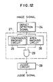
- Fig. 12 shows a first modification of the masking unit 27.
- a defect detection signal from the defect detection circuit 24 is supplied to the continuous masking unit 25 and the area masking circuit 26 so that the continuous masking the area-masking are performed parallelly.
- the continuous masking circuit 25 performs continuous masking on a defect detection signal to output a continuous masking signal
- the area masking circuit 26 performs the area-masking on the defect detection signal to output an area masking signal.
- An AND gate 29 gives a logical product of the continuous masking signal and an area masking signal of each point to supply an output signal to the judge circuit 28.
- the masking area Q for the area masking is 5 columns x 5 rows, and the smaller masking area q is 3 columns x 3 rows.
- These areas may be larger, e.g., the former may be 9 columns x 9 rows, and the latter being 5 columns x 5 rows.
- the masking area Q and the smaller masking area q may be horizontally elongate or vertically elongate.
- a horizontally elongate masking area Q exemplified in Fig. 14 prevents the erroneous detection of a joint R running vertically on the bottle 12 which was formed in manufacturing the bottle 12. That is, in the case where the direction of a matter, such as a joint R, which preferably is not detected as a defect is known beforehand, the masking area Q is set horizontal to the direction of the matter.
- the bottle continuously conveyed is followed by changing the optical axis of the two-dimensional photoelectric device 16, but instead a mirror is used to follow the bottle 12.
- the two dimensional photoelectric device 16 is used to detect a transmitted light image of the bottle 12, but instead a one dimensional photoelectric device, such as linear CCD, may be used.
- This invention is usable in detecting defects on the surface of, e.g., metal parts, plastics etc. other than bottles.
Landscapes
- Physics & Mathematics (AREA)
- Health & Medical Sciences (AREA)
- Life Sciences & Earth Sciences (AREA)
- Chemical & Material Sciences (AREA)
- Analytical Chemistry (AREA)
- Biochemistry (AREA)
- General Health & Medical Sciences (AREA)
- General Physics & Mathematics (AREA)
- Immunology (AREA)
- Pathology (AREA)
- Investigating Materials By The Use Of Optical Means Adapted For Particular Applications (AREA)
Description
- This invention relates to an apparatus for detecting defects on bottle sidewalls comprising illumination means to illuminate the sidewall of a bottle, photoelectrically converting means which converts a transmitted light image of the bottle into an electric analog signal, which is fed to an analog/digital converter means convert the electric analog signal into a digital signal, and a defect detecting means receives the digital signal to detect defects by comparing the brightnesses of at least two points to be inspected.
- It is necessary to inspect glass bottles containing liquors, beverages, foods, etc. for any defects whether they are newly made or have been recovered for reuses. The bottles are inspected on parts thereof, i.e., the bodies or sidewalls, bottoms, tops of the mouths and threaded bottle necks. Among these parts, the sidewalls tend to have defects, such as foreign matters or smears which may cause sanitary problems and cracks, scraches, seeds, blisters, etc. which may cause bottle breackages. It is necessary to inspect the bottles accurately for any these defects.
- From US-A-4492476 is known a defect detecting apparatus to determine the presence of defects in the sidewall of a bottle by illuminating the bottle, observing the illumination image transmitted through the sidewall using a two dimensional CCD device. The image of the rotated bottle is divided into picture elements arranged in a matrix form. The signals which represent the picture elements are generated sequentially and repeatedly. The signals of the picture elements on the same imaginary line perpendicular to the central axis of the image are compared with each other and the result of the comparison is used to detect a defect. There is not provided area masking means to subject a defect signals an area masking.
- The US-A-4454542 describes a defect detecting apparatus to form the image of an object under inspection. The image is divided ino a plurality of picture elements, the signals of which are stored and accumulated for each of the regions which form parts of the image. The results of the accumulated signals of the regions proximate to each other are compared and a defect is detected from the result of the comparison. The lines to divide the image in a plurality of regions are imagnarily drawn radially outwards from the center of the image. A second group of lines is interposed between a first group of lines. The defect signal is not subjected a further processing.
- Generally the apparatus for detecting defects on bottle sidewalls utilizes the fact that a portion of a defect appears darker than the other portion, in inspecting the sidewalls for defects. This apparatus has found it easy to detect defects, such as opaque foreign matters, etc. which are very light blocking, but has found it difficult to detect accurately defects, such as light smears, streaks, blisters, etc. which are opaque and are extended over large areas. With such generally used apparatus, the sensitivity of a photoelectric device is increased to detect these opaque large defects, consequently even noises due to different colors, different thicknesses of the sidewalls, etc. are detected as defects.
- A first object of this invention is to provide an apparatus for detecting defect on bottle sidewalls which can detect with high precision opaque defects which are thin and extend over large areas.
- A second object of this invention is to provide an apparatus for detecting defects on bottle sidewalls which can detect opaque defect which are thin and extend over large areas, without changing their contours.
- The first object can be achieved by an apparatus for detecting defects on bottle sidewalls as defined in the opening paragraph of the description, characterised in that an area masking means is connected in series or parallel with a continuous masking means which removes separate defect points and defect points which are continuous only below a set value as non-defects and outputs a fresh signal i.e. a continuous masking signal indicative of the presence/absence of a defect, a defect being indicated by outputting the continuous masking signal "1", wherein the defect detection means outputs a defect detection signal, indicative of the presence/absence of a defect from the brightness comparison made, to the area masking means and/or continuous masking means and the area masking means subjects the received signal to an area masking by which a rectangular masking area is set in which each point to be inspected is centered on a plurality of smaller masking areas, and outputting an area masking signal "1" directly, or via a logical gate means, which is connected to the area masking means and the continuous masking means, to a judging means, indicating that the point to be inspected is a defect when the number of points in the smaller masking areas for which the continuous masking signals are "1" is equal to or exceeds a set value, and wherein the judging means judges the presence of a defect on the sidewall of the bottle, based on the area masking signal from the area masking means. or the output signal from the logical gate means.
The second object can be achieved by an apparatus for detecting defects on bottle sidewalls as above defined, and wherein the masking area set by the area masking means is a rectangular area of m columns x n rows, the area masking means comprises at least a m-digit shift register for consecutively shifting the received continuous masking signals, a first adding circuit adds the values of n continuous masking signals received from the shift register, for each of the m columns of the masking area), at least m memories to consecutively store addition results of the first adding circuit, a second adding circuit to add the addition results stored in the memories, and a comparator which compares the sum of all addition results received from the second adding circuit with a set value to output an area masking signal "1" when the set value is exceeded and "0" when the set value is not exceeded. -
- Fig. 1 is a block diagram of the apparatus for detecting defects on bottle sidewalls according to a first embodiment of this invention;
- Fig. 2 is a view showing an inspection area and inspection gates for the apparatus for detecting defects on bottle sidewalls of Fig. 1;
- Fig. 3 is a view showing a masking area of an area masking circuit of the apparatus for detecting defects on bottle sidewalls of Fig. 1;
- Fig. 4 is a circuit diagram exemplifying the area masking circuit of the apparatus for detecting defect on bottle sidewalls of Fig. 1;
- Fig. 5 is a view explaining the operation of the area masking circuit;
- Figs. 6(a) and 6(b) are views showing results of masking noises and opaque defects in an image of light transmitted through a bottle sidewall;
- Fig. 7 is a block diagram of the apparatus for detecting defect on bottle sidewalls according to a second embodiment of this invention;
- Fig. 8 is a block diagram of a masking unit of the apparatus for detecting defects on bottle sidewalls of Fig. 7;
- Figs. 9 and 10 are views showing masking areas and smaller masking areas of the area masking of the apparatus for detecting defects on bottle sidewalls of Fig. 7;
- Figs. 11(a) and 11(b) are circuit diagrams exemplifying the area masking circuit of the apparatus for detecting detects on bottle sidewalls of Fig. 7;
- Fig. 12 is a block diagram of a first modification of the making unit of the apparatus for detecting defects on bottle sidewalls of Fig. 7;
- Fig. 13 is a view exemplifying the masking area.
- Fig. 1 shows the apparatus for detecting defects on bottle sidewalls according to a first embodiment of this invention.
- In this embodiment, a
bottle 12 to be inspected is continuously conveyed on rotation. Thebottle 1 is illuminated by adiffusion light source 10 having a surface for emitting even diffused lights. Adiffusion plate 10a for diffusing the illumination light is disposed on the front of thediffusion light source 10. An image of lights transmitted through the sidewall of thebottle 12 is formed in a two-dimensionalphotoelectric device 16. The two-dimensionalphotoelectric device 16 comprises a light detecting unit, such as an area CCD, for converting the transmitted light image into an electric analog signal, and an optical system for forming the transmitted light image of thebottle 12. - The optical
axis changing unit 14 is disposed in the optical axis of the two-dimensionalphotoelectric device 16 on the side nearer to thebottle 12 and changes the optical axis of the optical system with respect to the light detecting unit of the two-dimensionalphotoelectric device 16. The opticalaxis changing unit 14 changes the optical axis in synchronization with a movement of thebottle 12 so that a transmitted light image of thebottle 12 is formed in the light detecting unit of the two-dimensionalphotoelectic device 16. Specifically, adrive motor 15 swings horizontally alens 14a disposed on the front of the two-dimensionalphotoelectric device 16 by alens driving circuit 21 to change the optical axis. - An A/
D converter 18 converts an analog image signal from the two-dimensionalphotoelectric device 16 into a digital image signal of a given bits. This digital image signal is supplied to an inspection area/gate setting circuit 20, a monitordisplay RAM circuit 22 and adefect detection circuit 24. - The inspection area/
gate setting circuit 20 is for setting inspection areas in which thedefect detection circuit 24, which will be explained below, detects defects based on the transmitted light image as shown in Fig. 2. The inspection area may be determined based on the edges of the transmitted light image of thebottle 12 or may be fixedly determined beforehand. In Fig. 2, the inspection area is set on theentire bottle 12, and the inspection area is divided in fiveinspection gates bottle 12. The inspection area/gate setting circuit 20 supplies an inspecting gate signal to the monitordisplay RAM circuit 22, thedefect detection circuit 24, acontinuous masking circuit 25, anarea masking circuit 26 and ajudge circuit 28. - Based on the digital image signal from the A/
D converter 18, thedefect detection circuit 24 compares in brightness a plurality of points spaced from each other vertically and horizontally by a given distance to detect defects. Thedefect detection circuit 24 outputs a defect detection signal of "1" when a defect is present and outputs a defect detection signal of "0" when a defect is absent. - The defect detecting system for comparing a plurality of points in brightness includes a two-point defect detection system in which two point are compared in brightness to detect a defect, and a three-point detecting system in which three points are compared in brightness to detect a defect.
- In the two-point defect detecting system, when the following formula

- The three-point defect detecting system enables a defect to be detected without failure even when a transmitted light has uneven brightness. In this three-point defect detecting system, when the following formula

- It is also possible to detect a defect, based on a ratio between brightnesses QA and QB of two points A and B to be compared for detection. That is, when one of the following formulas


- It is also possible to detect a defect when one of the following formulas


- A defect detection signal outputted by the
defect detection circuit 24 is subjected to continuous masking by thecontinuous masking circuit 25. when thedefect detecting circuit 24 increases the sensitivity for the prevention of a defect detect ion error, sometimes thecircuit 24 erroneously detects none defective points as defect points. The continuous masking is for removing such erroneous defect points. At an actual defect appears continuous defect points having a size corresponding to that of the actual defect. Contrary to this, at a non-defect appears separate defect points. In this continuous masking, separate defect points, and defect points which are continuous only below a set value are removed as actually non-defects, and thecontinuous masking circuit 25 outputs a fresh continuous masking signal at each point. For example, when a defect point is actually a defect, a continuous masking signal of "1" is outputted, and when the defect point is not a defect, a continuous masking signal of "0" is outputted. - A continuous masking signal outputted by the
continuous masking circuit 25 is subjected to the area masking by anarea masking circuit 26. In the area masking, as shown in Fig. 3, a rectangular masking area Q of 5 rows x 5 columns is set with each point P centered, a number of points in the area Q at which (points) continuous masking signals are defects are added, and, based on whether or not a total number of defect points exceeds a set value, thearea masking circuit 26 outputs an area masking signal. That is, an area masking signal is generated only at a portion on which continuous masking signals are concentrated with noises appearing separately being removed. - Fig. 4 is an example of the
area masking circuit 26. - A continuous masking signal for each image is consecutively inputted to a
shift register 50 in synchronization with a clock pulse φ to be shifted and outputted. The digit number of theshift register 50 corresponds to a number of columns of the masking area Q. In the case where a screen has 500 pixels x 500 pixels as shown in Fig. 5, continuous masking signals are inputted to theshift register 50 first at the upper left end and then vertically downward. Theshift register 50 has anadder 51 which adds the values of 5 continuous masking signals. That is, a sum given by theadder 51 gives a sum of the continuous masking signals on each column of the masking region Q. - There are provided five
RAMs address counter 52. Data are written in the RAMs 61 - 65 throughrespective write gates 61w - 65w. It is designated by an output of a quinary ring counter 53 which writegate 61w - 65w data is written in. The ring counter 53 counts up by one every time theaddress counter 52 has outputted addresses from 0 to 499. - A sum given by the
adder 51 is written in bits of an address of one of the RAMs 61 - 65 designated by thering counter 65. The address of the RAMs 61 - 65 has been generated by theaddress counter 52. Accordingly the RAMs 61 - 65 store sums for every five vertically located continuous masking signals for adjacent five columns of the screen. - Data are read from the RAMs 61 - 65 through read gates 61r - 65r. All the read gates 61r - 65r are kept opened when data are read, so that the data of all the RAMs 61 - 65 including data being currently written are simultaneously read to be outputted to an
adder 54. - The
adder 54 adds the data read from the RAMs 61 - 65 and outputs an addition result to acomparator 55. Since the RAMs 61 - 65 correspond to the columns of the masking area Q, the addition result given by theadder 54 is a sum of all the continuous masking signals in the masking area Q. Thecomparator 55 compares this addition result with a set value to output a comparison result as an area masking signal. For example, when the set value is 18, the area masking signal becomes "1" only when the continuous masking signals of 18 or more points in the 5x5 masking area Q are "1", and when less than 18 points have "1", the area masking signal becomes "0". - The area masking circuit shown in Fig. 4 enables an area masking signal given by area-masking the 5x5 masking area Q to be obtained in real time only by inputting continuous masking signals consecutively in the
shift register 50. - The
judge circuit 28 judges the presence of a defect, based on an area masking signal from thearea masking circuit 26. For example, thejudge circuit 28 counts area masking signals of "1", and when a counted value exceeds a set value, thecircuit 28 judges thebottle 12 defective and supplies a judge signal a conveyor system (not shown) of thebottle 12. In response to the judge signal the conveyor system removes the defective bottle. - A
reference signal generator 30 generates a lens swing angle signal and an inspection period signal, based on a bottle position signal from abottle position detector 32 provided on a rotary table 13 on which thebottle 12 is mounted. The lens swing angle signal is for swinging aconcave lens 14a so that the transmitted light image of thebottle 12 is formed constantly on the two-dimensionalphotoelectric device 16 and is supplied to thelens drive circuit 21. Thelens drive circuit 21 swings theconcave lens 14a in accordance with a lens swing angle signal. The inspection period signal is indicative of a period in which theconcave lens 14a is swinging in accordance with a movement of thebottle 12 and is supplied to thejudge circuit 28. - Based on a lens swing angle signal from the
reference signal generator 30, thelens drive circuit 21 drives theconcave lens 14a. Thelens drive circuit 21 performs feedback control based on a swing angle signal from theconcave lens 14a as a feedback signal. When no swing angle signal is supplied by theconcave lens 14a, thelens drive circuit 21 performs the control in the open loop. - An inspection period signal from the
reference signal generator 30 is supplied to thejudge circuit 30. Thejudge circuit 28 takes as effective only the defect detection signals which are inputted thereto in a period in which the inspection period signal is high level to judge whether or not thebottle 12 is defective. It is also possible to supply an inspection period signal to the inspection area/gate setting circuit 20, thedefect detection circuit 24, and thecontinuous masking circuit 25 or thearea masking circuit 26 and take as effective only the inspection period signals which are inputted to thejudge circuit 28 in a period in which the inspection period signal is high level. - The monitor
display RAM circuit 22 stores a digital image signal of thebottle 12 in a frame memory built therein to display the image on amonitor 36. The monitordisplay RAM circuit 22 has been supplied with a defect detection signal from thearea masking circuit 26, a judge result signal from thejudge circuit 28, and an inspection gate signal from the inspection area/gate setting circuit 20. Based on the defect detection signal, a defect point or an error scan are written in the monitordisplay RAM circuit 22. Based on the inspection gate signal, a corresponding inspection gate is displayed on themonitor 36. - As described above, the continuous masking is followed by the area masking. This enables a defect to be detected without any errors even when noises are generated due to an increase in the sensitivity. That is, this is because the continuous masking signals indicative of noises are isolated as shown in Fig. 6(a), while the continuous masking signals indicative of opaque defects, such as light smears, streaks, blisters, etc., are scattered as shown in Fig. 6(b), which enables noises and opaque defects to be discriminated from each other.
- Fig. 7 shows the apparatus for detecting defects on bottle sidewalls according to a second embodiment of this invention. The members common with the first embodiment have share the same reference numerals not to repeat their explanations.
- The second embodiment is characterized by a masking
unit 27 for masking a defect detection signal from adefect detection circuit 24. - The masking
unit 27 of this embodiment is shown in Fig. 8 in good detail. - The masking
unit 27 comprises acontinuous masking circuit 25 and anarea masking circuit 26. A defect detection signal from thedefect detection circuit 24 is masked first by thecontinuous masking circuit 25, and then an output signal from thecontinuous masking circuit 25 is masked by thearea masking circuit 26. - The
continuous masking circuit 25 of this embodiment is the same as that of the first embodiment and omits as actually non-defects the defect points which are isolated or are continuous only below a set value to ouput a fresh continuous masking signal for each point. - A continuous masking signal from the
continuous masking circuit 25 is area-masked by thearea masking circuit 26, and an area masking signal is outputted. In the area-masking, a rectangular masking area Q of 5 rows x 5 columns, for example, is set with a point to be noted (P33) centered as shown in Fig. 9. Further, as shown in Fig. 10, in the masking area Q are set smaller masking areas q1 - q9 of, e.g., 3 rows x 3 columns with the point to be noted P33 contained. The numbers of defect points in the smaller masking areas q1 - q9 are added, and when the total number of defect points in one of the smaller masking areas exceed a set value NR, and further the point to be noted P (P33) is a defect point, the point to be noted P (P33) is found a defect point. - Such area masking generates an area masking signal only at a portion where defect points indicated by continuous masking signals are concentrated, while noises, which are indicated by isolated defect points, are removed. Accordingly the contour of a defect which has been area-masked is not much changed.
- An example of the
area masking circuit 26 is shown in Fig. 11. - Continuous masking signals for respective images are inputted consecutively to a flip-
flop 70 in synchronization with a clock signal φ and outputted. In the case of a 500 pixels x 500 pixels screen as shown in Fig. 5, for example, continuous masking signals are consecutively inputted in the flip-flop 70 first at the upper left end and vertically downward. - There are provided five
RAMS respective write gates 81w - 85w. It is designed by an output of a quinary ring counter 73 which writegate 81w - 85w data is written in. The ring counter 73 counts up by one every time the address counter 72 has outputted addresses from 0 to 499. - The continuous masking signals retained by the flip-
flop 70 are written in the one of the RAMs 81 - 85 designated by a ring counter 73 at bits of an address generated by an address counter 72. Accordingly, the RAMs 81 - 85 store continuous masking signals for adjacent 5 columns of the screen. - Continuous masking signals are read from the RAMs 81 - 85 through read
gates 81r - 85r. A continuous masking signal being currently written is read directly at aread gate 81r - 85r associated with the one of the readgates 81r - 85r designated by an output of a ring counter 73. At theother read gates 81r - 85r, continuous masking signal are read from the associated RAMs 81 - 85. To give an example, when the ring counter 73 designates the readgate 81w, and a continuous masking signal is being written in theRAM 81, the continuous masking signal currently being written is read directly at theread gate 81r, while the continuous masking signals stored in the RAMs 82r - 85r are read through read gates 82r - 85r. - The continuous masking signals read through the read
gates 81r - 85r are re-arranged in order by are-arranging circuit 90 to be stored in respective 5-digit shift registers 91 - 95. A number of digits of the shift registers 91 - 95 corresponds to a number of columns of the masking area Q. - The
re-arranging circuit 90 puts into another order the continuous masking signals read through the readgates 81r - 85r, based on an output from the ring counter 73 so that the outputs from the respective shift registers 91 - 95 are placed in a preset order of continuous masking signals as shown in Fig. 11. - By re-arranging continuous masking signals into another order by the re-arranging
circuit 90, output signals from the shift registers 91 - 95 becomes continuous masking signals P11 -P55 for the respective points of the masking area Q of Fig. 9. - There are provided adders 101 - 109 corresponding to the smaller masking areas q1 - q9 of Fig. 10, and the adders 101 - 109 add continuous masking siganls P11 - P55 for the points defining the respective smaller masking sreas q1 - q9 which are supplied by the shift registers 91 - 95. For example, the
adder 101 adds the continuous masking signals P11, P12, P13, P21, P22, P23, P31, P32 and P33 which define the smaller masking area q1 of Fig. 10(1). - Addition results of the adders 101 - 109 are compared with a set value NR by comparators 111 - 119. A nine-input OR
gate 120 gives a logical sum of comparison results of the comparators 111 - 119, and an AND gate gives a logical product of an output of theOR gate 120 with the continuous masking signal P33 of the point to be noted P. An output signal from the ANDgate 121 is an area masking signal. - To be specific, in the case where the set value NR is 5, only when five or more points of one of the 3x3 smaller masking areas q1 - q9 have continuous masking signals "1", and further the point to be noted P is a defect, the area masking signal becomes "1". Otherwise the area masking signal become "0".
- The area masking circuit of Fig. 11 enables an area masking signal which has been given by area-masking a 5x5 masking area Q to be obtained in real time only by inputting consecutively continuous masking signals to the flip-
flop 70. - A
judge circuit 28 judges the presence of a defect, based on an area masking signal supplied by thearea masking circuit 26. - In the embodiment described above, since whether or not a defect point is a defect is judged based on a number of defect points and a point to be noted in a smaller masking area, the area masking does not change the contour of a defect.
- Fig. 12 shows a first modification of the masking
unit 27. - In this modification, a defect detection signal from the
defect detection circuit 24 is supplied to thecontinuous masking unit 25 and thearea masking circuit 26 so that the continuous masking the area-masking are performed parallelly. Thecontinuous masking circuit 25 performs continuous masking on a defect detection signal to output a continuous masking signal, and thearea masking circuit 26 performs the area-masking on the defect detection signal to output an area masking signal. An ANDgate 29 gives a logical product of the continuous masking signal and an area masking signal of each point to supply an output signal to thejudge circuit 28. - This invention is not limited to the above-described embodiments and may cover variation which will be described below.
- To give an example, in the above-described first and second embodiments, the masking area Q for the area masking is 5 columns x 5 rows, and the smaller masking area q is 3 columns x 3 rows. These areas may be larger, e.g., the former may be 9 columns x 9 rows, and the latter being 5 columns x 5 rows.
- The masking area Q and the smaller masking area q may be horizontally elongate or vertically elongate. For example, a horizontally elongate masking area Q exemplified in Fig. 14 prevents the erroneous detection of a joint R running vertically on the
bottle 12 which was formed in manufacturing thebottle 12. That is, in the case where the direction of a matter, such as a joint R, which preferably is not detected as a defect is known beforehand, the masking area Q is set horizontal to the direction of the matter. - In the first embodiment, the bottle continuously conveyed is followed by changing the optical axis of the two-dimensional
photoelectric device 16, but instead a mirror is used to follow thebottle 12. - In the second embodiment, the two dimensional
photoelectric device 16 is used to detect a transmitted light image of thebottle 12, but instead a one dimensional photoelectric device, such as linear CCD, may be used. - This invention is usable in detecting defects on the surface of, e.g., metal parts, plastics etc. other than bottles.
Claims (7)
- An apparatus for detecting defects on bottle sidewalls comprising illumination means (10) to illuminate the sidewall of a bottle (12), photoelectrically converting means (16) which converts a transmitted light image of the bottle into an electric analog signal, which is fed to an analog/digital converter means (18) to convert the electric analog signal into a digital signal, and
a defect detecting means (24) receives the digital signal to detect defects by comparing the brightnesses of at least two points to be inspected; characterized in that an area masking means (26) is connected in series or parallel with a continuous masking means (25) which removes separate defect points and defect points which are continuous only below a set value as non-defects and outputs a fresh signal, i.e. a continuous masking signal indicative of the presence /absence of a defect, a defect being indicated by outputting the continuous masking signal "1" wherein the defect detection means (24) outputs a defect detection signal, indicative of the presence/absence of a defect from the brightness comparison made, to the area masking means and/or continuous masking means and the area masking means subjects the received signal to an area masking by which a rectangular masking area (Q) is set in which each point (P) to be inspected is centered on a plurality of smaller masking areas, and outputting an area masking signal "1" directly, or via a logical gate means (29), which is connected to the area masking means and the continuous masking means, to a judging means (28), indicating that the point to be inspected is a defect when the number of points in the smaller masking areas for which the continuous masking signals are "1" is equal to or exceeds a set value,and wherein the judging means (28) judges the presence of a defect on the sidewall of the bottle, based on the area masking signal from the area masking means (26;27) or the output signal from the logical gate means (29). - An apparatus for detecting defects on bottle sidewalls according to claim 1, wherein the area masking means (26) is connected via the continuous masking means (25) to the defect detection means (24), the connection being in series and wherein the continuous masking means (25) removes non-defect points which have been erroneously detected as defect points by the defect detection means (24).
- An apparatus for detecting defects on bottle sidewalls according to claim 2, wherein: the masking area (Q) set by the area masking means (26) is a rectangular area of m columns x n rows, the area masking means (26) comprises at least a m-digit shift register (50) for consecutively shifting the received continuous masking signals, a first adding circuit (51) adds the values of n continuous masking signals received from the shift register (50), for each of the m columns of the masking area (Q), at least m memories (61-65) to consecutively store addition results of the first adding circuit (51), a second adding circuit (54) to add the addition results stored in the memories, and a comparator (55) which compares the sum of all addition results received from the second adding circuit (54) with a set value to output an area masking signal "1" when the set value is exceeded and the "0" when the set value is not exceeded.
- An apparatus for detecting defects on bottle sidewalls according to claim 1, wherein each of the plurality of smaller masking areas (q1,...q9) contains the point (P) to be inspected and wherein the numbers of defect points in the smaller masking areas (q1,...q9) are added and if the total number of defect points in one of the smaller masking areas exceeds a set value and the point (P) to be inspected is a defect point, an area masking signal "1" is outputted, which indicates a defect point.
- An apparatus for detecting defects on bottle sidewalls according to claim 4 wherein the area masking circuit (26) comprises a re-arranging circuit (90) to re-arrange the order of the continuous masking signals (P11-P55) read-in m memories (81-85), the re-arranged continuous masking signals are fed from the re-arranging circuit (90) to shift registers (91-95) and the output signals from the shift registers are continuous masking signals (P11-P55) for the respective points of the masking area (Q).
- An apparatus for detecting defects on bottle sidewalls according to claim 4 or 5, wherein the area masking means (26) performs area masking by setting a rectangular masking area (Q) of columns and rows with each point (P) centered and corresponding to the respective outputted continuous masking signal.
- An apparatus for detecting defects on bottle sidewalls according to claim 4 or 5, wherein there is a masking unit (27) connected in series with the defect detection means (24) and the judging means (28), wherein the masking unit (27) comprises said continuous masking means (25) connected in parallel with said area masking means (26), the outputs of both means (25,26) being connected to a logical gate means (29) which supplies a logical product signal of the continuous masking signal from the continuous masking means (25) and of the area masking signal from the area masking means (26) to the judge means (28); and wherein the judging means (28) judges the presence of a defect on the sidewall of the bottle, when the logical product signal from the logical gate means (29) is "1".
Applications Claiming Priority (2)
| Application Number | Priority Date | Filing Date | Title |
|---|---|---|---|
| JP128247/88 | 1988-05-27 | ||
| JP63128247A JPH0641924B2 (en) | 1988-05-27 | 1988-05-27 | Defect detection device for bottle body |
Publications (3)
| Publication Number | Publication Date |
|---|---|
| EP0343664A2 EP0343664A2 (en) | 1989-11-29 |
| EP0343664A3 EP0343664A3 (en) | 1990-08-29 |
| EP0343664B1 true EP0343664B1 (en) | 1996-05-01 |
Family
ID=14980133
Family Applications (1)
| Application Number | Title | Priority Date | Filing Date |
|---|---|---|---|
| EP89109450A Expired - Lifetime EP0343664B1 (en) | 1988-05-27 | 1989-05-25 | Apparatus for detecting defects on bottle sidewalls |
Country Status (4)
| Country | Link |
|---|---|
| US (1) | US4948956A (en) |
| EP (1) | EP0343664B1 (en) |
| JP (1) | JPH0641924B2 (en) |
| DE (1) | DE68926362T2 (en) |
Families Citing this family (24)
| Publication number | Priority date | Publication date | Assignee | Title |
|---|---|---|---|---|
| JPH0736004B2 (en) * | 1990-09-19 | 1995-04-19 | 肇産業株式会社 | Inspection method and device |
| US5187376A (en) * | 1990-12-20 | 1993-02-16 | Toshiba Kikai Kabushiki Kaisha | Print monitoring apparatus with data processing |
| JPH0739999B2 (en) * | 1991-01-24 | 1995-05-01 | 肇産業株式会社 | Defect detection method |
| US5412203A (en) * | 1991-07-15 | 1995-05-02 | Fuji Electric Co., Ltd. | Cylindrical container inner surface tester |
| JP2756386B2 (en) * | 1991-12-27 | 1998-05-25 | 日本たばこ産業株式会社 | Visual inspection system for cylindrical objects |
| JP3044961B2 (en) * | 1993-02-12 | 2000-05-22 | 富士電機株式会社 | Circular container inner surface inspection device |
| DE59303013D1 (en) * | 1992-11-27 | 1996-07-25 | Elpatronic Ag | Process for separating reusable bottles from reusable circulation |
| US5466927A (en) * | 1994-04-08 | 1995-11-14 | Owens-Brockway Glass Container Inc. | Inspection of translucent containers |
| US5486692A (en) * | 1994-10-19 | 1996-01-23 | Emhart Glass Machinery Investments Inc. | Glassware inspection machine comprising diffused light sources and two-dimensional cameras |
| CH688663A5 (en) * | 1994-10-20 | 1997-12-31 | Elpatronic Ag | Method and apparatus for inspecting objects, particularly bottles. |
| US6025910A (en) * | 1995-09-12 | 2000-02-15 | Coors Brewing Company | Object inspection method utilizing a corrected image to find unknown characteristic |
| WO1997004887A1 (en) * | 1995-07-31 | 1997-02-13 | Coors Brewing Company | Hot bottle inspection apparatus and method |
| US6118526A (en) * | 1996-08-16 | 2000-09-12 | Coors Brewing Company | Method for measurement of light transmittance |
| US6025919A (en) * | 1996-08-16 | 2000-02-15 | Coors Brewing Company | Method for measurement of light transmittance |
| US6049379A (en) * | 1997-12-30 | 2000-04-11 | Coors Brewing Company | Method for inspecting translucent objects using imaging techniques |
| US5935285A (en) * | 1997-12-30 | 1999-08-10 | Coors Brewing Company | Method for inspecting manufactured articles |
| US6473169B1 (en) | 2000-05-03 | 2002-10-29 | Air Logic Power Systems, Inc. | Integrated leak and vision inspection system |
| US7342654B2 (en) * | 2003-12-19 | 2008-03-11 | International Business Machines Corporation | Detection of impurities in cylindrically shaped transparent media |
| EP1598662A1 (en) * | 2004-05-17 | 2005-11-23 | Total Petrochemicals Research Feluy | A method for quantifying the optical properties of moulded objects |
| US7060999B2 (en) | 2004-07-09 | 2006-06-13 | Owens-Brockway Glass Container Inc. | Apparatus and method for inspecting ribbed containers |
| US7595870B2 (en) * | 2004-11-10 | 2009-09-29 | Owens-Brockway Glass Container Inc. | Optical inspection of container walls |
| US7688437B2 (en) | 2007-05-02 | 2010-03-30 | Emhart Glass S.A. | Machine for inspecting glass containers |
| DE102009020919A1 (en) | 2009-05-12 | 2010-11-18 | Krones Ag | Device for detecting elevations and / or depressions on bottles, in particular in a labeling machine |
| DE102009020920A1 (en) | 2009-05-12 | 2010-11-18 | Krones Ag | Inspection device for detecting embossing and / or labels on transparent containers, in particular beverage bottles |
Family Cites Families (12)
| Publication number | Priority date | Publication date | Assignee | Title |
|---|---|---|---|---|
| JPS4934385A (en) * | 1972-07-28 | 1974-03-29 | ||
| JPS5546172A (en) * | 1978-09-29 | 1980-03-31 | Kirin Brewery Co Ltd | Detector for foreign material |
| US4300122A (en) * | 1979-04-02 | 1981-11-10 | Sperry Corporation | Apparatus for processing digital data representative of a two-dimensional image |
| US4492476A (en) * | 1981-02-20 | 1985-01-08 | Kirin Beer Kabushiki Kaisha | Defect detecting method and apparatus |
| JPS57178486A (en) * | 1981-04-25 | 1982-11-02 | Nippon Kogaku Kk <Nikon> | Smoothing device for binary image signal |
| JPS5821146A (en) * | 1981-07-30 | 1983-02-07 | Kirin Brewery Co Ltd | Method and device for inspection of defect |
| US4549205A (en) * | 1982-05-10 | 1985-10-22 | Takeda Chemical Industries, Ltd. | Ampoule inspecting method |
| JPH0612344B2 (en) * | 1982-08-31 | 1994-02-16 | サントリー株式会社 | Inspection device for scuffing bottles |
| IL79098A0 (en) * | 1985-07-15 | 1986-09-30 | Visionetics Corp | Fine flaw detector for printed circuit boards |
| US4742399A (en) * | 1985-11-01 | 1988-05-03 | Dainippon Screen Mfg. Co., Ltd. | Method of and apparatus for generating high-resolution bilevel image data |
| JPS6396095A (en) * | 1986-10-13 | 1988-04-26 | 株式会社キリンテクノシステム | Inspection device for screw mouth section of bottle |
| JPS63304146A (en) * | 1987-06-04 | 1988-12-12 | Kirin Brewery Co Ltd | Inspecting device for drum part of bottle |
-
1988
- 1988-05-27 JP JP63128247A patent/JPH0641924B2/en not_active Expired - Lifetime
-
1989
- 1989-05-25 DE DE68926362T patent/DE68926362T2/en not_active Expired - Fee Related
- 1989-05-25 EP EP89109450A patent/EP0343664B1/en not_active Expired - Lifetime
- 1989-05-26 US US07/357,288 patent/US4948956A/en not_active Expired - Lifetime
Also Published As
| Publication number | Publication date |
|---|---|
| DE68926362T2 (en) | 1996-12-12 |
| DE68926362D1 (en) | 1996-06-05 |
| JPH01299444A (en) | 1989-12-04 |
| EP0343664A3 (en) | 1990-08-29 |
| JPH0641924B2 (en) | 1994-06-01 |
| US4948956A (en) | 1990-08-14 |
| EP0343664A2 (en) | 1989-11-29 |
Similar Documents
| Publication | Publication Date | Title |
|---|---|---|
| EP0343664B1 (en) | Apparatus for detecting defects on bottle sidewalls | |
| EP0344617B1 (en) | Method and apparatus for inspecting sidewalls of bottles | |
| EP0597639B1 (en) | Non-contact surface flaw detection | |
| US4736851A (en) | Process and apparatus for the automatic inspection by transparency contrast in particular of containers | |
| US4579455A (en) | Photomask inspection apparatus and method with improved defect detection | |
| EP0200478A2 (en) | Glassware inspection using optical streak detection | |
| CA1175139A (en) | Defect detecting method and device | |
| US4492476A (en) | Defect detecting method and apparatus | |
| US5403722A (en) | Technique to count objects in a scanned image | |
| EP0483966B1 (en) | Method of and apparatus for inspecting a transparent or translucent article such as a bottle | |
| US4924083A (en) | Method and device for inspecting sidewall of bottle | |
| JP3497297B2 (en) | Inspection device for annular knurl area at container bottom | |
| JPH04220551A (en) | Method and apparatus for inspecting flaw of transparent body | |
| GB2104651A (en) | Defect detecting method and apparatus | |
| NO309213B1 (en) | Method and apparatus for inspecting liquid-filled containers | |
| US4549205A (en) | Ampoule inspecting method | |
| JPH0989805A (en) | Container inspection device with self-diagnosis function | |
| JPS63304146A (en) | Inspecting device for drum part of bottle | |
| EP0343665A2 (en) | Variable optical axis type bottle inspecting apparatus | |
| EP0438417A1 (en) | Inspection of container finish | |
| JPH06118026A (en) | Method for inspecting vessel inner surface | |
| JPH06103277B2 (en) | Defect detection device for bottle body | |
| JPS58132650A (en) | Method of detecting defect and device thereof | |
| JPH0432340B2 (en) | ||
| JPH02278145A (en) | Image flaw detection method and device |
Legal Events
| Date | Code | Title | Description |
|---|---|---|---|
| PUAI | Public reference made under article 153(3) epc to a published international application that has entered the european phase |
Free format text: ORIGINAL CODE: 0009012 |
|
| AK | Designated contracting states |
Kind code of ref document: A2 Designated state(s): DE FR GB |
|
| PUAL | Search report despatched |
Free format text: ORIGINAL CODE: 0009013 |
|
| AK | Designated contracting states |
Kind code of ref document: A3 Designated state(s): DE FR GB |
|
| RAP1 | Party data changed (applicant data changed or rights of an application transferred) |
Owner name: KABUSHIKI KAISHA KIRIN TECHNO SYSTEM |
|
| 17P | Request for examination filed |
Effective date: 19910221 |
|
| 17Q | First examination report despatched |
Effective date: 19920918 |
|
| GRAH | Despatch of communication of intention to grant a patent |
Free format text: ORIGINAL CODE: EPIDOS IGRA |
|
| GRAA | (expected) grant |
Free format text: ORIGINAL CODE: 0009210 |
|
| AK | Designated contracting states |
Kind code of ref document: B1 Designated state(s): DE FR GB |
|
| REF | Corresponds to: |
Ref document number: 68926362 Country of ref document: DE Date of ref document: 19960605 |
|
| ET | Fr: translation filed | ||
| PLBE | No opposition filed within time limit |
Free format text: ORIGINAL CODE: 0009261 |
|
| STAA | Information on the status of an ep patent application or granted ep patent |
Free format text: STATUS: NO OPPOSITION FILED WITHIN TIME LIMIT |
|
| 26N | No opposition filed | ||
| REG | Reference to a national code |
Ref country code: GB Ref legal event code: IF02 |
|
| PGFP | Annual fee paid to national office [announced via postgrant information from national office to epo] |
Ref country code: GB Payment date: 20040617 Year of fee payment: 16 |
|
| PGFP | Annual fee paid to national office [announced via postgrant information from national office to epo] |
Ref country code: FR Payment date: 20040618 Year of fee payment: 16 |
|
| PGFP | Annual fee paid to national office [announced via postgrant information from national office to epo] |
Ref country code: DE Payment date: 20040726 Year of fee payment: 16 |
|
| PG25 | Lapsed in a contracting state [announced via postgrant information from national office to epo] |
Ref country code: GB Free format text: LAPSE BECAUSE OF NON-PAYMENT OF DUE FEES Effective date: 20050525 |
|
| PG25 | Lapsed in a contracting state [announced via postgrant information from national office to epo] |
Ref country code: DE Free format text: LAPSE BECAUSE OF NON-PAYMENT OF DUE FEES Effective date: 20051201 |
|
| GBPC | Gb: european patent ceased through non-payment of renewal fee |
Effective date: 20050525 |
|
| PG25 | Lapsed in a contracting state [announced via postgrant information from national office to epo] |
Ref country code: FR Free format text: LAPSE BECAUSE OF NON-PAYMENT OF DUE FEES Effective date: 20060131 |
|
| REG | Reference to a national code |
Ref country code: FR Ref legal event code: ST Effective date: 20060131 |