EP0342900A1 - Herstellungsverfahren für Leuchtschirme - Google Patents
Herstellungsverfahren für Leuchtschirme Download PDFInfo
- Publication number
- EP0342900A1 EP0342900A1 EP89304890A EP89304890A EP0342900A1 EP 0342900 A1 EP0342900 A1 EP 0342900A1 EP 89304890 A EP89304890 A EP 89304890A EP 89304890 A EP89304890 A EP 89304890A EP 0342900 A1 EP0342900 A1 EP 0342900A1
- Authority
- EP
- European Patent Office
- Prior art keywords
- layer
- resist
- mask
- faceplate
- electron
- Prior art date
- Legal status (The legal status is an assumption and is not a legal conclusion. Google has not performed a legal analysis and makes no representation as to the accuracy of the status listed.)
- Withdrawn
Links
- OAICVXFJPJFONN-UHFFFAOYSA-N Phosphorus Chemical compound [P] OAICVXFJPJFONN-UHFFFAOYSA-N 0.000 title claims abstract description 66
- 238000010894 electron beam technology Methods 0.000 claims abstract description 46
- 238000000034 method Methods 0.000 claims abstract description 34
- 230000000903 blocking effect Effects 0.000 claims abstract description 30
- 238000003491 array Methods 0.000 claims abstract description 28
- 230000001678 irradiating effect Effects 0.000 claims abstract description 14
- 239000000463 material Substances 0.000 claims abstract description 14
- 239000011230 binding agent Substances 0.000 claims description 13
- 238000005086 pumping Methods 0.000 claims description 5
- 230000000717 retained effect Effects 0.000 claims description 5
- 239000010410 layer Substances 0.000 claims 30
- 239000011241 protective layer Substances 0.000 claims 1
- 239000011248 coating agent Substances 0.000 description 15
- 238000000576 coating method Methods 0.000 description 15
- 239000000203 mixture Substances 0.000 description 7
- 229920002120 photoresistant polymer Polymers 0.000 description 7
- VYZAMTAEIAYCRO-UHFFFAOYSA-N Chromium Chemical compound [Cr] VYZAMTAEIAYCRO-UHFFFAOYSA-N 0.000 description 5
- 229910052804 chromium Inorganic materials 0.000 description 4
- 239000011651 chromium Substances 0.000 description 4
- 239000003086 colorant Substances 0.000 description 4
- 238000012864 cross contamination Methods 0.000 description 4
- XLYOFNOQVPJJNP-UHFFFAOYSA-N water Substances O XLYOFNOQVPJJNP-UHFFFAOYSA-N 0.000 description 4
- HEMHJVSKTPXQMS-UHFFFAOYSA-M Sodium hydroxide Chemical compound [OH-].[Na+] HEMHJVSKTPXQMS-UHFFFAOYSA-M 0.000 description 3
- 239000011521 glass Substances 0.000 description 3
- 239000004922 lacquer Substances 0.000 description 3
- 238000004519 manufacturing process Methods 0.000 description 3
- 239000002002 slurry Substances 0.000 description 3
- 239000002904 solvent Substances 0.000 description 3
- QGZKDVFQNNGYKY-UHFFFAOYSA-O Ammonium Chemical compound [NH4+] QGZKDVFQNNGYKY-UHFFFAOYSA-O 0.000 description 2
- VVQNEPGJFQJSBK-UHFFFAOYSA-N Methyl methacrylate Chemical compound COC(=O)C(C)=C VVQNEPGJFQJSBK-UHFFFAOYSA-N 0.000 description 2
- 230000002745 absorbent Effects 0.000 description 2
- 239000002250 absorbent Substances 0.000 description 2
- 238000005530 etching Methods 0.000 description 2
- VCJMYUPGQJHHFU-UHFFFAOYSA-N iron(3+);trinitrate Chemical compound [Fe+3].[O-][N+]([O-])=O.[O-][N+]([O-])=O.[O-][N+]([O-])=O VCJMYUPGQJHHFU-UHFFFAOYSA-N 0.000 description 2
- VLTRZXGMWDSKGL-UHFFFAOYSA-N perchloric acid Chemical compound OCl(=O)(=O)=O VLTRZXGMWDSKGL-UHFFFAOYSA-N 0.000 description 2
- 229920003229 poly(methyl methacrylate) Polymers 0.000 description 2
- QTBSBXVTEAMEQO-UHFFFAOYSA-M Acetate Chemical compound CC([O-])=O QTBSBXVTEAMEQO-UHFFFAOYSA-M 0.000 description 1
- UIERETOOQGIECD-UHFFFAOYSA-N Angelic acid Natural products CC=C(C)C(O)=O UIERETOOQGIECD-UHFFFAOYSA-N 0.000 description 1
- 239000004642 Polyimide Substances 0.000 description 1
- 239000004372 Polyvinyl alcohol Substances 0.000 description 1
- AZDRQVAHHNSJOQ-UHFFFAOYSA-N alumane Chemical group [AlH3] AZDRQVAHHNSJOQ-UHFFFAOYSA-N 0.000 description 1
- XAGFODPZIPBFFR-UHFFFAOYSA-N aluminium Chemical compound [Al] XAGFODPZIPBFFR-UHFFFAOYSA-N 0.000 description 1
- 239000004411 aluminium Substances 0.000 description 1
- 229910052782 aluminium Inorganic materials 0.000 description 1
- 239000000919 ceramic Substances 0.000 description 1
- 239000003795 chemical substances by application Substances 0.000 description 1
- 239000004020 conductor Substances 0.000 description 1
- 238000011109 contamination Methods 0.000 description 1
- 238000007796 conventional method Methods 0.000 description 1
- 229920001577 copolymer Polymers 0.000 description 1
- SOCTUWSJJQCPFX-UHFFFAOYSA-N dichromate(2-) Chemical compound [O-][Cr](=O)(=O)O[Cr]([O-])(=O)=O SOCTUWSJJQCPFX-UHFFFAOYSA-N 0.000 description 1
- 230000000694 effects Effects 0.000 description 1
- 230000005686 electrostatic field Effects 0.000 description 1
- 238000001704 evaporation Methods 0.000 description 1
- 230000008020 evaporation Effects 0.000 description 1
- AMGQUBHHOARCQH-UHFFFAOYSA-N indium;oxotin Chemical compound [In].[Sn]=O AMGQUBHHOARCQH-UHFFFAOYSA-N 0.000 description 1
- 238000003780 insertion Methods 0.000 description 1
- 230000037431 insertion Effects 0.000 description 1
- 150000002734 metacrylic acid derivatives Chemical class 0.000 description 1
- 229910052751 metal Inorganic materials 0.000 description 1
- 239000002184 metal Substances 0.000 description 1
- VHRYZQNGTZXDNX-UHFFFAOYSA-N methacryloyl chloride Chemical compound CC(=C)C(Cl)=O VHRYZQNGTZXDNX-UHFFFAOYSA-N 0.000 description 1
- 239000005022 packaging material Substances 0.000 description 1
- 229920001721 polyimide Polymers 0.000 description 1
- 239000004926 polymethyl methacrylate Substances 0.000 description 1
- 235000019422 polyvinyl alcohol Nutrition 0.000 description 1
- 229920002451 polyvinyl alcohol Polymers 0.000 description 1
- 235000011121 sodium hydroxide Nutrition 0.000 description 1
- 238000009987 spinning Methods 0.000 description 1
- UIERETOOQGIECD-ONEGZZNKSA-N tiglic acid Chemical compound C\C=C(/C)C(O)=O UIERETOOQGIECD-ONEGZZNKSA-N 0.000 description 1
- XOLBLPGZBRYERU-UHFFFAOYSA-N tin dioxide Chemical compound O=[Sn]=O XOLBLPGZBRYERU-UHFFFAOYSA-N 0.000 description 1
- 229910001887 tin oxide Inorganic materials 0.000 description 1
- 238000005406 washing Methods 0.000 description 1
Images


Classifications
-
- H—ELECTRICITY
- H01—ELECTRIC ELEMENTS
- H01J—ELECTRIC DISCHARGE TUBES OR DISCHARGE LAMPS
- H01J9/00—Apparatus or processes specially adapted for the manufacture, installation, removal, maintenance of electric discharge tubes, discharge lamps, or parts thereof; Recovery of material from discharge tubes or lamps
- H01J9/20—Manufacture of screens on or from which an image or pattern is formed, picked up, converted or stored; Applying coatings to the vessel
- H01J9/22—Applying luminescent coatings
- H01J9/227—Applying luminescent coatings with luminescent material discontinuously arranged, e.g. in dots or lines
- H01J9/2271—Applying luminescent coatings with luminescent material discontinuously arranged, e.g. in dots or lines by photographic processes
Definitions
- the present invention relates to a method of preparing a phosphor screen.
- a colour cathode ray tube comprises a screen on which arrays of different phosphors which emit differently coloured light in response to electron beams, are accurately positioned on a screen of the CRT with respect to holes (or slits) in a shadow mask.
- An electron gun arrangement produces a different electron beam for each colour.
- Many methods of making the arrays of phosphors are known.
- U.S. Patent 4251610 discloses an illustrative method in which an opaque layer is first formed on the inner surface of holes in a black opaque layer. Assuming three differently “coloured” phosphors are to be used, three arrays of holes are produced in the opaque layer. This is done by coating the opaque layer with photo resist, and illuminating the coating through a shadow mask with light from a light source which simulates the three electron beams, developing the resist, etching the layer using the developed resist as a mask and then removing the resist.
- Phosphor of one colour e.g. green is put into one of the arrays using the following process:-
- a coating of photo resist is put over the entire opaque layer and the holes.
- the coating is exposed to ultra-violet (UV) light from a light source simulating the green electron beam through the shadow mask.
- UV ultra-violet
- the coating is then developed to expose the "green” array of holes leaving the two other arrays covered by resist.
- Green phosphor and photosensitive binder are put onto the screen.
- the phosphor and binder are exposed to ultra violet light through the screen to fix the green phosphor in the green holes. Excess phosphor, binder and photoresist are removed, leaving an array of green phosphor dots.
- the process is repeated for the other colours. Each repetition begins with a new coating of photo resist which covers the previously laid-down phosphor, thus protecting the previously laid-down phosphor from cross-contamination.
- an opaque layer is first formed on the inner surface of the screen of a CRT.
- An array of phosphor is laid down using the following process:-
- the layer is coated with electron beam sensitive resist which is exposed to e.g. the "green” electron beam through a shadow mask.
- the electron beam resist is developed and the layer etched to produce an array of "green” apertures or holes thereon.
- Green" phosphor plus photosensitive binder is applied and is exposed to UV light through the screen to fix the phosphor in the apertures.
- the electron beam resist is removed.
- a new coating of electron beam resist is then laid down and the process repeated for the or each other coloured phosphor.
- a phosphor screen having accurate placement of the phosphors, and preferably also with reduced cross-contamination of the phosphors.
- a method of forming a plurality of different interspersed arrays of phosphors on the inside of a faceplate for a colour cathode ray tube in which method, a first mask is formed by irradiating an electron sensitive resist layer through a shadow mask with an electron gun arrangement in a demountable tube substantially at the same positions with respect to the arrays as the electron gun arrangement which will energise those arrays in the completed tube, a layer of light blocking material is formed over the first mask, subsidiary masks are sequentially formed in the blocking layer for respective ones of the arrays of phosphors, each subsidiary mask being formed by irradiating electron beam resist covering the blocking layer through the shadow mask with an electron beam corresponding to the beam which will energise the associated array in use of the tube and removing the irradiated resist and underlying blocking layer, and phosphor is fixed in position in the sub-mask.
- each sub-mask and phosphor array is covered by the resist layer used for making the next sub-mask before the next sub-mask and phosphor array is formed, all the resist layers being retained until all the phosphor arrays are formed.
- the phosphors are fixed in position by irradiating them with light through the sub-masks.
- the light is preferably UV light and the blocking layer blocks UV light.
- a method of forming a plurality of interspersed colour phosphor arrays on the inside of a faceplate for a colour cathode ray tube comprising;
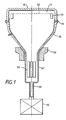
- FIG. 1 illustrates a "demountable" CRT system, which accurately simulates the completed CRT, using the actual CRT faceplate 101 and its matching shadow mask 102 and shadow mask frame 103.
- the envelope 104 which may be made of metal, glass or ceramic and which is connected by a tube 105 to a vacuum pump system 106.
- a multiple electron gun 108 Inside the neck of the envelope 104 is mounted a multiple electron gun 108 and on the exterior of the neck 107 are mounted the CRT scan coils 109 by which the electron beams emitted by the electron gun 108 can be made to scan by the application of the appropriate voltage waveforms.
- the whole assembly within the envelope 104 is vacuum tight, the faceplate 101 being joined to the envelope 104 by means of a gasket 110.
- the faceplate 1 of the CRT is separated from the shadow mask 102 and an opaque coating 2 is applied.
- the coating which is conductive may be reflective, for example aluminium, or may be a black coating, for example a layer of black chromium (which is non-conductive) together with a conductive material such as indium tin oxide or tin oxide.
- the black chromium is applied by evaporation in an oxidising gassy atmosphere by methods which are well known and long established.
- a first layer of electron sensitive resist 3 is then applied to the faceplate 1 for example by spinning.
- the resist layer is then hardened by baking.
- the type of resist may be described as "positive” or “negative” according to whether it softens or hardens respectively under the action of an electron beam; for convenience the method here described is the process for the "positive” resist).
- Various types of electron sensitive resist may be used, for example, one comprising copolymers of methylmethacrylic acid and methacryloyl chloride and other methacrylates i.e. PM type resists.
- PM type resists Alternatively, PMMA types of electron sensitive resist comprising polymethylmethacrylates in cellusolve acetate may be used.
- a particular commercially available electron sensitive resist which may be used is ISOFINE E-B positive resist grade P7.
- the faceplate 1 and the shadow mask 102 are then assembled together and placed on the demountable CRT as in Figure 1. Appropriate voltages are applied and the resist 3 is exposed, through the shadow mask 102 to scanning electron beams from the directions indicated by the arrows in Figure 2-3 from all of the electron guns in the electron gun housing 108. Those parts of the resist 3 which receive the electron beam through the shadow mask holes become softened.
- the faceplate assembly is then removed from the demountable CRT and the resist layer 3 is treated with developer, whereupon the exposed dots or lines, as appropriate, are removed and the unexposed areas remain to produce an opaque layer 2 on the faceplate 1 with an apertured layer of developed resist 3 superimposed thereon.
- the exposed parts of the opaque layer 2 are then etched away through the apertures or holes in the resist 3, and the unexposed parts of the opaque layer 2 are allowed to remain, as shown in Figure 2-4, thus forming a mask having apertures 5 therein.
- the opaque layer 30 is black chromium then the etching agent used can be a mixture of ammonium ferric nitrate, perchloric acid and demineralised water. If aluminium forms the opaque layer 30 then this can be etched using dilute caustic soda.
- a mask containing apertures or holes e.g. dots or lines, for red, green and blue emitting phosphors.
- the remaining layer of resist 3 and the apertures 5 are coated firstly with a blocking layer of material which blocks (or absorbs) ultra-violet light, and secondly with a layer of electron beam resist over the blocking layer.
- the coating is indicated by reference 6.
- the blocking layer is for example a coating called Anti-Reflection Coating (ARC) obtainable from Brewer Science Inc. of (address please).
- ARC comprises heavily dyed polyimide and is a highly UV light absorbing coating.
- D ARC also available from Brewer Science Inc.
- the blocking layer must be compatible with the electron beam resist, survive baking, and block UV light. To be compatible with the resist it must at least not inhibit the resist and preferably also be miscible with the resist.
- the faceplate 1 is then reunited with the shadowmask 102 and the assembly is placed on the demountable tube shown in Figure 1.
- the tube is pumped down to vacuum, and one, e.g. green, of the electron guns is energised to expose the resist 6 over the "green" apertures 5 to the "green" beam GB (Fig 2-6).
- the assembly is then removed from the tube and the resist 6 is developed. Developing the resist 6 removes the resist 6 from the "green” holes; in addition the ARC in the "green” holes may be simultaneously removed. Alternatively, the ARC can be removed from the "green” holes in a separate developing step.
- Fig 2-6 ARC and resist 6 is left in the "red” and "blue” holes and over the mask of black chrome.
- U.V. sensitive photobinder for example, polyvinylalcohol sensitised with ammonium bichromate
- a second layer of electron sensitive resist 8 is now applied.
- the second layer of resist 8 covers the e.g. green phosphor and the first layer of resist and ARC 6.
- the faceplate 1 together with the shadow mask 102 are then assembled together and placed on the demountable CRT shown in Figure 1 and the first 6 and second 8 layers of resist are exposed, through the shadow mask 2 to a scanning electron beam from the direction indicated by the arrows in Figure 2-9.
- a different one of the electron guns is used to generate the beam RB in this case, for example, the gun responsible for the red content on the screen.
- first and second layers of resist 6, 8 which receive the electron beam RB through the shadow mask holes become softened and, as before, the faceplate assembly is then removed from the demountable CRT and the first and second resist layers 6 and 8 are treated with developer, whereupon the exposed dots or lines 35 of resist 6, 8 are removed and the unexposed areas remain. Additionally, where the apertures 35 of resist 6, 8 are removed, the ARC is also removed.
- the faceplate is exposed to U.V from a diffuse source shone through the glass faceplate 1 so that the parts of the photoresist and phosphor mixture which are in the apertures 35 are polymerised.
- the ARC prevents the mixture polymerising elsewhere.
- Developing the photobinder results in hardened phosphor dots or lines remaining in the apertures 10 as shown in Figure 2-12.
- the first layer of ARC and electron sensitive resist 6 is retained, and the second layer of resist 8 is also retained.
- the process is repeated by applying a third layer of resist over the first and second layers and over the red and green phosphors.
- the third layer is exposed to the "blue" electron gun through the shadow mask, and developed, the opaque layer etched and "blue” phosphor fixed in the apertures as described above. The result is shown in Figure 2-13.
- arrays of the red, green and blue phosphors 33′, 36 and 37 are arranged in interspersed relation on the faceplate 1 in registry with the points at which the red, green and blue electron beams, respectively, irradiate the faceplate 1 during use.
- the second repeat of the process may be omitted if required to produce a screen with only two colours of phosphor. Similarly, further repeats may be necessary to produce a screen with more than three colours.
- each phosphor to be fixed in position is protected from cross-contamination by the other phosphors.
- Electron-sensitive resists are normally insufficiently absorbent to act as masks to the UV light themselves even when two or more layers of resist are present with U.V absorbing dye.
- the ARC however, makes possible the process in which all the sets of apertures are formed in the mask simultaneously.
- red, green and blue phosphors Whilst reference has been made to red, green and blue phosphors, other colours of phosphor can be used, e.g. yellow, magenta and cyan.
- Figure 3 shows an alternative method, in accordance with a further aspect of the invention, for preparing a phosphor screen and which avoids irradiating phosphor through the black absorbing layer as shown in Figures 2-7 to 2-13.
- the starting point for the process shown in Figure 3 is a mask of e.g. black chromium formed on the faceplate 1 using the steps shown in Figures 2-1, 2-2, 2-3 and 2-4 as described above.
- the mask 2 is thus formed using the electron beams to produce three arrays of apertures for the red, green and blue phosphors.
- the mask is covered in e.g. a slurry of green phosphor 7 as shown in Figure 3-2.
- the shadow mask 102 is then remounted on the faceplate and the assembly of faceplate and shadow mask is then exposed, in a known form of light house, to ultra violet light corresponding to e.g. the green electron beam.
- the light irradiates the phosphor slurry 7 through the shadow mask and activates the green phosphor at positions corresponding to positions which would be irradiated by the green elcctron gun in use of the faceplate.
- the faceplate is disassembled from the light house and shadow mask and the excess phosphor removed with water or the appropriate solvent leaving the green dots or lines 9 as shown in Figure 3-4.
- the mask 2 and the green dots or lines are then coated with a thin layer or lacquer of material such as methylmethacrylate, a slurry of e.g. red phosphor and photobinder 10 is then laid down.
- the shadow mask 102 is then reassembled into the faceplate, the assembly is then assembled into a light house and irradiated with ultra violet light corresponding to the red electron beam.
- the irradiated red phosphor is washed with water or the appropriate solvent leaving the red dot array, a further lacquer of methylmethacrylate provided over the mask 2 and the red and green dots or lines and the process repeated for the third e.g. blue phosphor.
- the electron beam resist layers, lacquers and photosensitive binders are removed by baking.
- the phosphor screen is lacquered and aluminised by conventional means.
Landscapes
- Engineering & Computer Science (AREA)
- Manufacturing & Machinery (AREA)
- Formation Of Various Coating Films On Cathode Ray Tubes And Lamps (AREA)
Applications Claiming Priority (2)
| Application Number | Priority Date | Filing Date | Title |
|---|---|---|---|
| GB8811914 | 1988-05-20 | ||
| GB8811914A GB2218846A (en) | 1988-05-20 | 1988-05-20 | Manufacture of colour crt phoshor screen |
Publications (1)
| Publication Number | Publication Date |
|---|---|
| EP0342900A1 true EP0342900A1 (de) | 1989-11-23 |
Family
ID=10637202
Family Applications (1)
| Application Number | Title | Priority Date | Filing Date |
|---|---|---|---|
| EP89304890A Withdrawn EP0342900A1 (de) | 1988-05-20 | 1989-05-15 | Herstellungsverfahren für Leuchtschirme |
Country Status (3)
| Country | Link |
|---|---|
| EP (1) | EP0342900A1 (de) |
| JP (1) | JPH0221536A (de) |
| GB (1) | GB2218846A (de) |
Citations (3)
| Publication number | Priority date | Publication date | Assignee | Title |
|---|---|---|---|---|
| EP0091163A2 (de) * | 1982-04-02 | 1983-10-12 | North American Philips Corporation | Positiv arbeitende Photoresistmasse und Verfahren zur Herstellung einer lichtabsorbierenden Schwarzmatrix in einer Farbbildröhre |
| EP0135965A2 (de) * | 1983-09-12 | 1985-04-03 | North American Philips Consumer Electronics Corp. | Photographisches Verfahren zum Aufbringen eines Phosphormusters auf eine Schattenmaske eines Farb-Kathodenstrahlungsrohrs |
| GB2176647A (en) * | 1985-03-26 | 1986-12-31 | Rank Electronic Tubes Ltd | Manufacture of colour CRT phosphor screens |
-
1988
- 1988-05-20 GB GB8811914A patent/GB2218846A/en not_active Withdrawn
-
1989
- 1989-05-15 EP EP89304890A patent/EP0342900A1/de not_active Withdrawn
- 1989-05-19 JP JP12772889A patent/JPH0221536A/ja active Pending
Patent Citations (3)
| Publication number | Priority date | Publication date | Assignee | Title |
|---|---|---|---|---|
| EP0091163A2 (de) * | 1982-04-02 | 1983-10-12 | North American Philips Corporation | Positiv arbeitende Photoresistmasse und Verfahren zur Herstellung einer lichtabsorbierenden Schwarzmatrix in einer Farbbildröhre |
| EP0135965A2 (de) * | 1983-09-12 | 1985-04-03 | North American Philips Consumer Electronics Corp. | Photographisches Verfahren zum Aufbringen eines Phosphormusters auf eine Schattenmaske eines Farb-Kathodenstrahlungsrohrs |
| GB2176647A (en) * | 1985-03-26 | 1986-12-31 | Rank Electronic Tubes Ltd | Manufacture of colour CRT phosphor screens |
Non-Patent Citations (1)
| Title |
|---|
| PATENT ABSTRACTS OF JAPAN, unexamined applications, E field, vol. 8, no. 221, October 9, 1984 THE PATENT OFFICE JAPANESE GOVERNMENT page 121 E 271 * |
Also Published As
| Publication number | Publication date |
|---|---|
| GB2218846A (en) | 1989-11-22 |
| GB8811914D0 (en) | 1988-06-22 |
| JPH0221536A (ja) | 1990-01-24 |
Similar Documents
| Publication | Publication Date | Title |
|---|---|---|
| US4251610A (en) | Method of making multicolor CRT display screen with minimal phosphor contamination | |
| US3569761A (en) | Color phosphor electroluminescent screen with filters for color cathode-ray display tubes | |
| US3615462A (en) | Processing black-surround screens | |
| US4049451A (en) | Method for forming a color television picture tube screen | |
| US5730887A (en) | Display apparatus having enhanced resolution shadow mask and method of making same | |
| US3779760A (en) | Method of producing a striped cathode ray tube screen | |
| US2897089A (en) | Method of printing color phosphor patterns | |
| US4070498A (en) | Method of manufacturing fluorescent screen of color picture tube | |
| US3406068A (en) | Photographic methods of making electron-sensitive mosaic screens | |
| US3726678A (en) | Method of screening a color picture tube | |
| US3067349A (en) | Method for producing registered color screen cathode-ray tubes | |
| EP0342900A1 (de) | Herstellungsverfahren für Leuchtschirme | |
| EP0322200A1 (de) | Verfahren zur Herstellung eines Leuchtschirmes | |
| US4223083A (en) | Virtual mask exposure system for CRT screen manufacture | |
| GB2176647A (en) | Manufacture of colour CRT phosphor screens | |
| US3080231A (en) | Process for photographically forming color screens | |
| US3734728A (en) | Method of screening a color picture tube | |
| US4778738A (en) | Method for producing a luminescent viewing screen in a focus mask cathode-ray tube | |
| US3767395A (en) | Multiple exposure color tube screening | |
| US3736137A (en) | Aperture mask for,and method of screening,a color cathode-ray tube | |
| US3677758A (en) | Screening a black-surround color cathode-ray tube | |
| US3224895A (en) | Method of manufacturing display screens for cathode-ray tubes | |
| JPS61232538A (ja) | 色基準用モノクロ陰極線管およびその製造方法 | |
| US3499372A (en) | Cathode ray tube screen exposure | |
| JP4073045B2 (ja) | 無孔マトリクス周縁部に被着した蛍光体素子を有するカラー陰極線管 |
Legal Events
| Date | Code | Title | Description |
|---|---|---|---|
| PUAI | Public reference made under article 153(3) epc to a published international application that has entered the european phase |
Free format text: ORIGINAL CODE: 0009012 |
|
| AK | Designated contracting states |
Kind code of ref document: A1 Designated state(s): DE FR IT NL |
|
| STAA | Information on the status of an ep patent application or granted ep patent |
Free format text: STATUS: THE APPLICATION IS DEEMED TO BE WITHDRAWN |
|
| 18D | Application deemed to be withdrawn |
Effective date: 19900524 |