EP0342466A2 - Statischer RAM-Speicher mit Immunität gegen Einzelereignisse - Google Patents
Statischer RAM-Speicher mit Immunität gegen Einzelereignisse Download PDFInfo
- Publication number
- EP0342466A2 EP0342466A2 EP89108234A EP89108234A EP0342466A2 EP 0342466 A2 EP0342466 A2 EP 0342466A2 EP 89108234 A EP89108234 A EP 89108234A EP 89108234 A EP89108234 A EP 89108234A EP 0342466 A2 EP0342466 A2 EP 0342466A2
- Authority
- EP
- European Patent Office
- Prior art keywords
- transistor means
- single event
- nodes
- drain
- radiation
- Prior art date
- Legal status (The legal status is an assumption and is not a legal conclusion. Google has not performed a legal analysis and makes no representation as to the accuracy of the status listed.)
- Withdrawn
Links
Images
Classifications
-
- G—PHYSICS
- G11—INFORMATION STORAGE
- G11C—STATIC STORES
- G11C11/00—Digital stores characterised by the use of particular electric or magnetic storage elements; Storage elements therefor
- G11C11/21—Digital stores characterised by the use of particular electric or magnetic storage elements; Storage elements therefor using electric elements
- G11C11/34—Digital stores characterised by the use of particular electric or magnetic storage elements; Storage elements therefor using electric elements using semiconductor devices
- G11C11/40—Digital stores characterised by the use of particular electric or magnetic storage elements; Storage elements therefor using electric elements using semiconductor devices using transistors
- G11C11/41—Digital stores characterised by the use of particular electric or magnetic storage elements; Storage elements therefor using electric elements using semiconductor devices using transistors forming static cells with positive feedback, i.e. cells not needing refreshing or charge regeneration, e.g. bistable multivibrator or Schmitt trigger
- G11C11/412—Digital stores characterised by the use of particular electric or magnetic storage elements; Storage elements therefor using electric elements using semiconductor devices using transistors forming static cells with positive feedback, i.e. cells not needing refreshing or charge regeneration, e.g. bistable multivibrator or Schmitt trigger using field-effect transistors only
- G11C11/4125—Cells incorporating circuit means for protecting against loss of information
-
- G—PHYSICS
- G11—INFORMATION STORAGE
- G11C—STATIC STORES
- G11C5/00—Details of stores covered by group G11C11/00
- G11C5/005—Circuit means for protection against loss of information of semiconductor storage devices
Definitions
- This invention relates in general to an improved random access memory and in particular to a static random access memory with an improved technique for immunizing the memory to single event upsets due to an ionizing radiation hit.
- static RAMs are less sensitive to single event upsets, such as ion penetration, than are dynamic RAMs
- the data in conventional static RAM circuits without any immunity or radiation hardness can be destroyed in the event of ion penetration. This is because certain radiation impulses can cause the RAM memory latch to make unplanned state changes from which the circuit is unable to recover once the radiation is no longer present.
- resistors are put into the memory cell to harden the circuit to radiation impulses
- the resistors have been found to create additional problems due to the large variation in their value. It is difficult to control the actual value of a resistor because of its sensitivity to temperature and because of variations in the processing of the resistors, i.e., doping levels, line widths, etc.
- resistive hardened circuits may impose certain restraints on the memory circuit, such as an upper limit of approximately 50-100 MHz on the frequency of the latch operation, this technique of employing the resistors does not appreciably increase the circuit real estate or area. Such a feature is desirable in fabricating memory devices. Therefore, prior to the present invention, the decoupling resistor technique was the best technique known for immunizing a RAM to single event upsets.
- semiconductor memory device which incorporates a coupling capacitor between the two storage nodes to achieve radiation hardness of the circuit.
- the invention eliminates the undesirable side effects of resistive hardening such as the increased response time of the circuit.
- the invention also make permits to use of a capacitor which is more stable over process variations and temperature variations than are resistors. Furthermore, the capacitor does not require any additional die area.
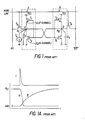
- Figure 1 typifies the problem occurring in static RAMs where no immunity is provided against single event upset.
- Figure 1 has two standard CMOS inverters A and B. Each inverter is balanced with a storage node and the same number of N and P channel transistors T1-T6.
- Nodes N1 and N2 are storage nodes for data and its complement, data .
- Each of nodes N1 and N2 has a parasitic or stray capacitance, C s .
- the current source, I represents the impulse caused by a radiation hit to the Q side of the memory latch, i.e. to node N1.
- Figure 1A illustrates what happens to the voltages at nodes N1 and N2 when the RAM cell is penetrated by an ionizing radiation hit.
- This hit generates a current impulse, I, which causes the Q side of the memory latch to discharge from a logic "1" level to ground, allowing the Q side of the latch to go high.
- I current impulse
- the RAM has no protection against the outside interference and false data can be written in the memory to compromise its usefulness.
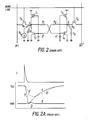
- Figure 2 illustrates the well known prior art technique for protecting the Figure 1 RAM against interference from outside radiation sources.
- Figure 2 has two standard CMOS inverters which are balanced on each side with storage nodes N1 and N2 and the same number of N-channel and P-channel transistors.
- the Figure 2 circuit has been supplied with decoupling resistors R1 and R2. Resistors R1 and R2 must be of a value sufficient to delay the transition period for the Q′ and Q ′ nodes after the Q and Q nodes respectively.
- Figure 2A plots the voltage drop over nodes N1 and N2 where there is a decoupling resistor between the two nodes to delay their write cycle. As illustrated, the voltage waveforms for Q′ and Q ′ do not cross and therefore the memory cell recovers to its original logic state after the radiation pulse is finished. Even though this technique of resistive hardening against radiation interference is viable, there are enough disadvantages and undesirable side effects of this resistive hardening technique such that a more desirable technique is warranted.
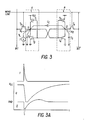
- the invention as set forth in Figure 3 provides for a more desirable alternative to the resistive hardening technique against radiation interference.
- the memory device is only vulnerable when a single event ion or outside radiation interference hits the storage node when the node is in the logic "1" state. That is, if a single event ion or radiation interference should hit a data storage node N1 in the logic "0" state, there will be no detrimental effect on the circuit.
- resistors R1 and R2 have been replaced with a coupling capacitor C c across the Q′ and Q ′ nodes.
- the voltage across Cc cannot change instantaneously, thus adding the potential for greater stability to the circuit in the event of a single event upset.
- the voltage drop at N2 is limited by the P-N diode clamping between the transistor drain and the substrate or well. This clamps the voltage at N2 to approximately one diode voltage drop below ground.
- both sides of the CMOS latch have a logic "0" input even though the two stages (inverters A and B) are being driven by different voltages. This is an unstable condition for the latch and both stages of the latch will initially attempt to drive high.
- the output of node N2 is approximately one diode drop lower than the output of N1 the inherent voltage gain of the cross-coupled latch will drive these nodes to their correct levels assuming the latch has been properly designed and balanced, i.e.
- N1 will achieve its original logic state of "1” before N2 is able to go high. AsN1 achieves a logic state of "1”, it will drive N2 back to its logic state of "0" and the inverters will both resume their logic states prior to the radiation interference.
- the minimum size of the coupling capacitor Cc may be determined by the inequality A typical coupling capacitor may be equal to half Cs.
- the invention has been described with specific applications primarily directed to radiation hardening for static RAMs, it is anticipated that the invention may also be applied to the hardening of latches in general, e.g., storage registers, shift registers, counters, etc. Furthermore, the invention may have applications outside of the area of radiation hardening. For example, the invention may be used to improve the immunity of a memory cell to power supply glitches for poly-load-resistor RAMs. This increased stability will become critically important as memory cells shrink in size with each generation of technology advancement.
Landscapes
- Engineering & Computer Science (AREA)
- Microelectronics & Electronic Packaging (AREA)
- Computer Hardware Design (AREA)
- Static Random-Access Memory (AREA)
- Semiconductor Memories (AREA)
- Semiconductor Integrated Circuits (AREA)
Applications Claiming Priority (2)
| Application Number | Priority Date | Filing Date | Title |
|---|---|---|---|
| US19445588A | 1988-05-16 | 1988-05-16 | |
| US194455 | 1988-05-16 |
Publications (2)
| Publication Number | Publication Date |
|---|---|
| EP0342466A2 true EP0342466A2 (de) | 1989-11-23 |
| EP0342466A3 EP0342466A3 (de) | 1990-11-28 |
Family
ID=22717665
Family Applications (1)
| Application Number | Title | Priority Date | Filing Date |
|---|---|---|---|
| EP19890108234 Withdrawn EP0342466A3 (de) | 1988-05-16 | 1989-05-08 | Statischer RAM-Speicher mit Immunität gegen Einzelereignisse |
Country Status (2)
| Country | Link |
|---|---|
| EP (1) | EP0342466A3 (de) |
| JP (1) | JPH02103795A (de) |
Cited By (2)
| Publication number | Priority date | Publication date | Assignee | Title |
|---|---|---|---|---|
| SG86973A1 (en) * | 1992-10-27 | 2002-03-19 | Motorola Inc | Static random access memory resistant to soft error |
| US6737712B2 (en) | 1995-07-18 | 2004-05-18 | Hitachi, Ltd. | Method of manufacturing semiconductor integrated circuit device having capacitor element |
Families Citing this family (1)
| Publication number | Priority date | Publication date | Assignee | Title |
|---|---|---|---|---|
| US7397692B1 (en) | 2006-12-19 | 2008-07-08 | International Business Machines Corporation | High performance single event upset hardened SRAM cell |
Family Cites Families (1)
| Publication number | Priority date | Publication date | Assignee | Title |
|---|---|---|---|---|
| EP0098417A3 (de) * | 1982-06-15 | 1986-12-30 | Kabushiki Kaisha Toshiba | Halbleiterspeicheranordnung |
-
1989
- 1989-05-08 EP EP19890108234 patent/EP0342466A3/de not_active Withdrawn
- 1989-05-16 JP JP1120591A patent/JPH02103795A/ja active Pending
Cited By (6)
| Publication number | Priority date | Publication date | Assignee | Title |
|---|---|---|---|---|
| SG86973A1 (en) * | 1992-10-27 | 2002-03-19 | Motorola Inc | Static random access memory resistant to soft error |
| US6737712B2 (en) | 1995-07-18 | 2004-05-18 | Hitachi, Ltd. | Method of manufacturing semiconductor integrated circuit device having capacitor element |
| US7030449B2 (en) | 1995-07-18 | 2006-04-18 | Renesas Technology Corp. | Semiconductor integrated circuit device having capacitor element |
| US7199433B2 (en) | 1995-07-18 | 2007-04-03 | Renesas Technology Corp. | Method of manufacturing semiconductor integrated circuit device having capacitor element |
| US7323735B2 (en) | 1995-07-18 | 2008-01-29 | Renesas Technology Corp. | Method of manufacturing semiconductor integrated circuit device having capacitor element |
| US7598558B2 (en) | 1995-07-18 | 2009-10-06 | Renesas Technology Corp. | Method of manufacturing semiconductor integrated circuit device having capacitor element |
Also Published As
| Publication number | Publication date |
|---|---|
| EP0342466A3 (de) | 1990-11-28 |
| JPH02103795A (ja) | 1990-04-16 |
Similar Documents
| Publication | Publication Date | Title |
|---|---|---|
| EP1088310B1 (de) | Strahlengeschützter 6-transistorenspeicher mit wahlfreiem zugriff und speicherbauelement | |
| US4130892A (en) | Radiation hard memory cell and array thereof | |
| US4852060A (en) | Soft error resistant data storage cells | |
| US5111429A (en) | Single event upset hardening CMOS memory circuit | |
| US5525923A (en) | Single event upset immune register with fast write access | |
| US6326809B1 (en) | Apparatus for and method of eliminating single event upsets in combinational logic | |
| US5065048A (en) | Semiconductor logic circuit with noise suppression circuit | |
| US6278287B1 (en) | Isolated well transistor structure for mitigation of single event upsets | |
| US5418473A (en) | Single event upset immune logic family | |
| US5905290A (en) | Single event upset hardened memory cell | |
| US5307142A (en) | High performance static latches with complete single event upset immunity | |
| EP0217601B1 (de) | Speicherzelle | |
| US8116120B2 (en) | Depletion-mode MOSFET circuit and applications | |
| US6870408B2 (en) | Power-up circuit | |
| US5334888A (en) | Fast exclusive-or and exclusive-nor gates | |
| US6058041A (en) | SEU hardening circuit | |
| US4725981A (en) | Random access memory cell resistant to inadvertant change of state due to charged particles | |
| EP0574094B1 (de) | Speichervorrichtungen | |
| EP0130910B1 (de) | Leseverstärker | |
| US5087835A (en) | Positive edge triggered synchronized pulse generator | |
| US4514829A (en) | Word line decoder and driver circuits for high density semiconductor memory | |
| EP0887935B1 (de) | Störisolierungsschaltung | |
| US5118968A (en) | Special mode activation circuit for selectively activating a special mode circuit of a semiconductor integrated circuit device | |
| EP0232038B1 (de) | Integrierte Halbleiterschaltung mit Erkennungsschaltung für Adressensignal-Wechsel | |
| US4858182A (en) | High speed zero power reset circuit for CMOS memory cells |
Legal Events
| Date | Code | Title | Description |
|---|---|---|---|
| PUAI | Public reference made under article 153(3) epc to a published international application that has entered the european phase |
Free format text: ORIGINAL CODE: 0009012 |
|
| AK | Designated contracting states |
Kind code of ref document: A2 Designated state(s): DE FR GB IT NL |
|
| PUAL | Search report despatched |
Free format text: ORIGINAL CODE: 0009013 |
|
| AK | Designated contracting states |
Kind code of ref document: A3 Designated state(s): DE FR GB IT NL |
|
| RHK1 | Main classification (correction) |
Ipc: G11C 5/00 |
|
| 17P | Request for examination filed |
Effective date: 19910404 |
|
| 17Q | First examination report despatched |
Effective date: 19930105 |
|
| STAA | Information on the status of an ep patent application or granted ep patent |
Free format text: STATUS: THE APPLICATION IS DEEMED TO BE WITHDRAWN |
|
| 18D | Application deemed to be withdrawn |
Effective date: 19930518 |