EP0341768A2 - EPROM-Speicher, der aus einer einzigen Niederspannungsnetzversorgung entnommene Programmierungsspannungen benutzt - Google Patents
EPROM-Speicher, der aus einer einzigen Niederspannungsnetzversorgung entnommene Programmierungsspannungen benutzt Download PDFInfo
- Publication number
- EP0341768A2 EP0341768A2 EP89201022A EP89201022A EP0341768A2 EP 0341768 A2 EP0341768 A2 EP 0341768A2 EP 89201022 A EP89201022 A EP 89201022A EP 89201022 A EP89201022 A EP 89201022A EP 0341768 A2 EP0341768 A2 EP 0341768A2
- Authority
- EP
- European Patent Office
- Prior art keywords
- voltage
- power supply
- control gate
- programming
- eprom memory
- Prior art date
- Legal status (The legal status is an assumption and is not a legal conclusion. Google has not performed a legal analysis and makes no representation as to the accuracy of the status listed.)
- Withdrawn
Links
- 230000015654 memory Effects 0.000 title claims abstract description 22
- 239000000758 substrate Substances 0.000 claims abstract description 4
- 239000004065 semiconductor Substances 0.000 claims abstract description 3
- VYPSYNLAJGMNEJ-UHFFFAOYSA-N Silicium dioxide Chemical compound O=[Si]=O VYPSYNLAJGMNEJ-UHFFFAOYSA-N 0.000 description 3
- 230000005684 electric field Effects 0.000 description 3
- 229910052814 silicon oxide Inorganic materials 0.000 description 3
- 230000006870 function Effects 0.000 description 2
- 238000005036 potential barrier Methods 0.000 description 2
- XUIMIQQOPSSXEZ-UHFFFAOYSA-N Silicon Chemical compound [Si] XUIMIQQOPSSXEZ-UHFFFAOYSA-N 0.000 description 1
- 239000000969 carrier Substances 0.000 description 1
- 229910052710 silicon Inorganic materials 0.000 description 1
- 239000010703 silicon Substances 0.000 description 1
Images
Classifications
-
- G—PHYSICS
- G11—INFORMATION STORAGE
- G11C—STATIC STORES
- G11C16/00—Erasable programmable read-only memories
- G11C16/02—Erasable programmable read-only memories electrically programmable
- G11C16/04—Erasable programmable read-only memories electrically programmable using variable threshold transistors, e.g. FAMOS
- G11C16/0408—Erasable programmable read-only memories electrically programmable using variable threshold transistors, e.g. FAMOS comprising cells containing floating gate transistors
- G11C16/0416—Erasable programmable read-only memories electrically programmable using variable threshold transistors, e.g. FAMOS comprising cells containing floating gate transistors comprising cells containing a single floating gate transistor and no select transistor, e.g. UV EPROM
-
- G—PHYSICS
- G11—INFORMATION STORAGE
- G11C—STATIC STORES
- G11C16/00—Erasable programmable read-only memories
- G11C16/02—Erasable programmable read-only memories electrically programmable
- G11C16/06—Auxiliary circuits, e.g. for writing into memory
- G11C16/30—Power supply circuits
Definitions
- the present invention relates to an EPROM memory which uses programming voltages taken from a single low voltage power supply.
- nonvolatile EPROM memories use memory cells consisting of MOS transistors comprising a semiconductor substrate provided with source and drain areas with an interposed channel area, a control gate and a floating gate completely immersed in silicon oxide between the control gate and the channel area.
- MOS transistors comprising a semiconductor substrate provided with source and drain areas with an interposed channel area, a control gate and a floating gate completely immersed in silicon oxide between the control gate and the channel area.
- a negative electric charge constituting the memorized information.
- thermoionic emission of the electrons circulating in the MOS transistor channel directing the carriers emitted to the floating gate by means of an appropriate electrical field generated by applying to the drain and control gate appropriate programming voltages.
- a voltage such as to take the transistor into saturation.
- a high voltage is also applied to the control gate of the cell in such a manner as to create an electrical field perpendicular to the channel, which is capable of directing the accelerated electrons to the floating gate.
- the object of the present invention is to achieve an EPROM memory not requiring for programming a power supply voltage different from that otherwise provided for normal operation of the memory.
- an EPROM memory characterized in that it uses for programming a drain voltage no higher than the power supply voltage normally used for operation of the memory and a control gate voltage taken from said power supply voltage through a voltage booster.
- a single low power supply voltage the one used for normal operation of the memory, is capable of supplying both the voltages necessary for programming the memory.
- At least three important advantages are provided by the present invention as follows: (a) saving of a pin in the memory package, (b) the possibility of on-board programming without having to provide a particular power supply to be used only for said programming, and (c) greater strength of the integrated circuit due to the fact that the high programming voltage applied to the control gate is not supplied by an outside feeder capable of supplying power so that it is easier to protect the device from the eventuality of an overvoltage in the programming phase which could damage it permanently.
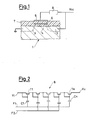
- an EPROM memory cell comprising a silicon substrate 1 provided with drain 2 and source 3 areas with an interposed channel area 4, a control gate 5 and a floating gate 6 completely immersed in silicon oxide 7 between the control gate 5 and the channel area 4.
- the source area 3 is connected to ground while the drain area 2 is connected to the normal power supply voltage Vcc of 5V.
- Vcc normal power supply voltage
- To the control gate 5 is applied a higher programming voltage, 12.5V, also taken from the power supply voltage Vcc through a voltage booster 8.
- the voltage booster 8 may be of any known type, e.g. as shown in FIG. 2, where T1-Tn are MOS transistors of the growth type, C1-Cn are condensers, F1 and F2 are the control phases of the voltage boosters, Vi is the input voltage and Vu is the output voltage.
- T1-Tn MOS transistors of the growth type
- C1-Cn condensers
- F1 and F2 are the control phases of the voltage boosters
- Vi the input voltage
- Vu is the output voltage.
- the relationship between the output and input voltages depends on the voltages of the control phase voltages F1, F2 in addition to the design data of the transistors T1-Tn and the condensers C1-Cn.
Landscapes
- Engineering & Computer Science (AREA)
- Microelectronics & Electronic Packaging (AREA)
- Non-Volatile Memory (AREA)
- Read Only Memory (AREA)
Applications Claiming Priority (2)
| Application Number | Priority Date | Filing Date | Title |
|---|---|---|---|
| IT20540/88A IT1217565B (it) | 1988-05-11 | 1988-05-11 | Memoria eprom utilizzante tensioni di programmazione ricavate da un'unica bassa tensione di alimentazione |
| IT2054088 | 1988-05-11 |
Publications (2)
| Publication Number | Publication Date |
|---|---|
| EP0341768A2 true EP0341768A2 (de) | 1989-11-15 |
| EP0341768A3 EP0341768A3 (de) | 1991-10-02 |
Family
ID=11168487
Family Applications (1)
| Application Number | Title | Priority Date | Filing Date |
|---|---|---|---|
| EP19890201022 Withdrawn EP0341768A3 (de) | 1988-05-11 | 1989-04-20 | EPROM-Speicher, der aus einer einzigen Niederspannungsnetzversorgung entnommene Programmierungsspannungen benutzt |
Country Status (3)
| Country | Link |
|---|---|
| EP (1) | EP0341768A3 (de) |
| JP (1) | JPH02223098A (de) |
| IT (1) | IT1217565B (de) |
-
1988
- 1988-05-11 IT IT20540/88A patent/IT1217565B/it active
-
1989
- 1989-04-20 EP EP19890201022 patent/EP0341768A3/de not_active Withdrawn
- 1989-05-09 JP JP1114369A patent/JPH02223098A/ja active Pending
Non-Patent Citations (2)
| Title |
|---|
| IEEE JOURNAL OF SOLID-STATE CIRCUITS. vol. SC-19, no. 1, February 1984, NEW YORK US pages 135 - 143; MC CREARY ET AL.: 'TECHNIQUES FOR A 5V-ONLY 64K EPROM BASED UPON SUBSTRATE HOT-ELECTRON INJECTION ' * |
| INTERNATIONAL ELECTRONIC DEVICES MEETING December 1983, WASHINGTON, DC USA pages 570 - 573; OHYA ET AL.: 'SINGLE 5V EPROM WITH SUB-MICRON MEMORY TRANSISTOR AND ON-CHIP HIGH VOLTAGE GENERATOR ' * |
Also Published As
| Publication number | Publication date |
|---|---|
| JPH02223098A (ja) | 1990-09-05 |
| EP0341768A3 (de) | 1991-10-02 |
| IT1217565B (it) | 1990-03-30 |
| IT8820540A0 (it) | 1988-05-11 |
Similar Documents
| Publication | Publication Date | Title |
|---|---|---|
| US4511811A (en) | Charge pump for providing programming voltage to the word lines in a semiconductor memory array | |
| CN1389874B (zh) | 使用非易失性单元的单个单元可编程切换器 | |
| US4321489A (en) | Voltage detection circuit | |
| EP0305937A1 (de) | MOS-Eingangs-/Ausgangsschutz unter Benutzung eines Entwurfs mit umschaltbarem Körperpotential | |
| EP0284724A2 (de) | Halbleiter-Festwertspeichereinrichtung | |
| WO1997012444B1 (en) | Programmable logic device with configurable power supply | |
| EP1217626A1 (de) | NMOS-Transistor vom Anreicherungstyp | |
| US5805502A (en) | System for constant field erasure in a FLASH EPROM | |
| US6392463B1 (en) | Electrical load driving circuit with protection | |
| US5903498A (en) | Low-supply-voltage nonvolatile memory device with voltage boosting | |
| US5309402A (en) | Flash electrically erasable and programmable ROM | |
| US6285238B1 (en) | Electrically programmable fuse | |
| US6867464B2 (en) | Supply voltage reduction circuit for integrated circuit | |
| US4455493A (en) | Substrate bias pump | |
| US4451748A (en) | MOS High voltage switching circuit | |
| US4581672A (en) | Internal high voltage (Vpp) regulator for integrated circuits | |
| US4317051A (en) | Clock generator (buffer) circuit | |
| US20020131302A1 (en) | NAND stack EEPROM with random programming capability | |
| EP0559995B1 (de) | Dekodierschaltung fähig zur Ubertragung von positiven und negativen Spannungen | |
| US5047675A (en) | Circuit device, made up of a reduced number of components, for simultaneously turning on a plurality of power transistors | |
| KR100278725B1 (ko) | 제1전압 부스팅 회로를 가진 집적회로 | |
| US6137315A (en) | Drive circuit for a non-volatile semiconductor storage configuration | |
| US6091657A (en) | Integrated circuit having protection of low voltage devices | |
| EP0758129B1 (de) | Flash-EEPROM mit integrierter Anordnung zur Begrenzung der Löschung der Source-Spannung | |
| CA1252520A (en) | High reliability complementary logic |
Legal Events
| Date | Code | Title | Description |
|---|---|---|---|
| PUAI | Public reference made under article 153(3) epc to a published international application that has entered the european phase |
Free format text: ORIGINAL CODE: 0009012 |
|
| AK | Designated contracting states |
Kind code of ref document: A2 Designated state(s): DE FR GB NL SE |
|
| RAP1 | Party data changed (applicant data changed or rights of an application transferred) |
Owner name: SGS-THOMSON MICROELECTRONICS S.R.L. |
|
| PUAL | Search report despatched |
Free format text: ORIGINAL CODE: 0009013 |
|
| AK | Designated contracting states |
Kind code of ref document: A3 Designated state(s): DE FR GB NL SE |
|
| STAA | Information on the status of an ep patent application or granted ep patent |
Free format text: STATUS: THE APPLICATION IS DEEMED TO BE WITHDRAWN |
|
| 18D | Application deemed to be withdrawn |
Effective date: 19920403 |