EP0341576A2 - Self-checking capacitive proximity switch - Google Patents
Self-checking capacitive proximity switch Download PDFInfo
- Publication number
- EP0341576A2 EP0341576A2 EP89108068A EP89108068A EP0341576A2 EP 0341576 A2 EP0341576 A2 EP 0341576A2 EP 89108068 A EP89108068 A EP 89108068A EP 89108068 A EP89108068 A EP 89108068A EP 0341576 A2 EP0341576 A2 EP 0341576A2
- Authority
- EP
- European Patent Office
- Prior art keywords
- electrode
- proximity switch
- oscillator
- test
- sensor electrode
- Prior art date
- Legal status (The legal status is an assumption and is not a legal conclusion. Google has not performed a legal analysis and makes no representation as to the accuracy of the status listed.)
- Granted
Links
Images

Classifications
-
- H—ELECTRICITY
- H03—ELECTRONIC CIRCUITRY
- H03K—PULSE TECHNIQUE
- H03K17/00—Electronic switching or gating, i.e. not by contact-making and –breaking
- H03K17/94—Electronic switching or gating, i.e. not by contact-making and –breaking characterised by the way in which the control signals are generated
- H03K17/945—Proximity switches
- H03K17/955—Proximity switches using a capacitive detector
Landscapes
- Electronic Switches (AREA)
- Switches That Are Operated By Magnetic Or Electric Fields (AREA)
Abstract
Description
Die Erfindung betrifft einen selbstprüfenden Näherungsschalter mit einem durch Annäherung eines Gegenstandes an seine Sensorfläche beeinflußbaren Oszillator, dem ein Demodulator und eine Triggerstufe nachgeschaltet sind, mit einer kapazitiv an den Oszillator angekoppelten Prüfimpulsquelle zur Erzeugung von Prüfimpulsen, deren Amplitude ausreichend hoch ist, um bei mindestens einem Schaltzustand der Triggerstufe ein Kippen derselben in den anderen ihrer beiden Schaltzustände herbeizuführen, und mit einer auf die in Abhängigkeit von den Prüfimpulsen auftretenden Pegeländerungen des Ausgangssignals der Triggerstufe ansprechenden, der Erzeugung eines Prüfausgangssignals dienenden Prüfschaltung.The invention relates to a self-testing proximity switch with an oscillator which can be influenced by the approach of an object to its sensor surface and which is followed by a demodulator and a trigger stage, with a test pulse source capacitively coupled to the oscillator for generating test pulses whose amplitude is sufficiently high to be at least one Switching state of the trigger stage to bring about a tilting of the same in the other of its two switching states, and with a test circuit which is responsive to the level changes in the output signal of the trigger stage which occur as a function of the test pulses and which serves to generate a test output signal.
Ein selbstprüfender Näherungsschalter dieser Art, und zwar ein induktiver Näherungsschalter, ist aus der DE-OS 33 27 188 bekannt. Bei diesem bekannten, induktiven Näherungsschalter wird die Prüfimpulsquelle insbesondere kapazitiv an den Speisespannungskreis des Oszillatorverstärkers angekoppelt. Als Prüfimpulse dienen bei dem bekannten Näherungsschalter bipolare Doppelimpulse, von denen ein Einzelimpuls der einen Polarität ein Absinken der Amplitude der Oszillatorschwingung bewirkt, während der darauf folgende Einzelimpuls entgegengesetzter Polarität eine Erhöhung der Amplitude der Oszillatorschwingung bewirkt. Dabei wird die Amplitude der Prüfimpulse einerseits und die Lage der Triggerschwellen des Näherungsschalters andererseits so gewählt, daß bei bedämpftem und unbedämpftem Oszillator jeweils durch einen der Einzelimpulse jedes Doppelimpulses eine Änderung des Triggerausgangssignals herbeigeführt wird.A self-checking proximity switch of this type, namely an inductive proximity switch, is known from DE-OS 33 27 188. In this known, inductive proximity switch, the test pulse source is coupled, in particular, capacitively to the supply voltage circuit of the oscillator amplifier. In the known proximity switch, bipolar double pulses serve as test pulses, of which a single pulse of one polarity causes the amplitude of the oscillator oscillation to decrease, while the subsequent single pulse of opposite polarity causes an increase in the amplitude of the oscillator oscillation. The amplitude of the test pulses on the one hand and the position of the trigger thresholds of the proximity switch on the other hand are selected so that when the oscillator is damped and undamped, a change in the trigger output signal is brought about by one of the individual pulses of each double pulse.
Ausgehend von diesem Stand der Technik liegt der Erfindung die Aufgabe zugrunde, die Fehlersicherheit eines Näherungsschalters der eingangs angegebenen Art noch weiterzuverbessern.
Diese Aufgabe wird bei einem gattungsgemäßen Näherungsschalter gemäß der Erfindung dadurch gelöst, daß der Näherungsschalter als kapazitiver Näherungsschalter mit einer an die Sensorfläche angrenzenden Sensorelektrode ausgebildet ist, die mit dem Steuereingang eines Oszillatorverstärkers verbunden ist und daß das Einkoppeln der mit Hilfe der Prüfimpulsquelle erzeugten Prüfimpulse, insbesondere an der Basis eines den Oszillatorverstärker bildenden Transistors erfolgt.Proceeding from this prior art, the object of the invention is to further improve the fault safety of a proximity switch of the type specified at the outset.
This object is achieved in a generic proximity switch according to the invention in that the proximity switch is designed as a capacitive proximity switch with a sensor electrode adjacent to the sensor surface, which is connected to the control input of an oscillator amplifier, and in that the coupling of the test pulses generated with the aid of the test pulse source, in particular at the base of a transistor forming the oscillator amplifier.
Dadurch, daß die Prüfimpulse bei dem erfindungsgemäßen Näherungsschalter am Steuereingang des Oszillatorverstärkers, insbesondere an der Basis des Oszillatortransistors,eingekoppelt werden, ergibt sich der wichtige Vorteil, daß auch die einwandfreie Funktion des Verstärkers bzw. des Transistors selbst überwacht wird. Dabei können die Prüfimpulse direkt an den Basisanschluß des Oszillatortransistors angelegt werden.
Besonders günstig ist es jedoch in Ausgestaltung der Erfindung, wenn die Prüfimpulsquelle mit einer zusätzlichen zweiten Elektrode verbunden ist, die in unmittelbarer Nähe der Sensorelektrode angeordnet ist. In diesem Fall können die Prüfimpulse kapazitiv über die durch die Sensorelektrode und die zusätzliche Elektrode gebildete Koppelkapazität eingekoppelt werden, wobei die Sensorelektrode direkt mit der Basis des Oszillatortransistors verbunden ist, so daß nicht nur die Funktion des Oszillatortransistors, sondern darüber hinaus auch das Vorhandensein einer einwandfreien Verbindung zwischen der Sensorelektrode und der Basis des Ozillatortransistors überwacht wird.Because the test pulses in the proximity switch according to the invention are coupled in at the control input of the oscillator amplifier, in particular at the base of the oscillator transistor, there is the important advantage that the proper functioning of the amplifier or the transistor itself is also monitored. The test pulses can be applied directly to the base connection of the oscillator transistor.
In an embodiment of the invention, however, it is particularly favorable if the test pulse source is connected to an additional second electrode, which is arranged in the immediate vicinity of the sensor electrode. In this case, the test pulses can be capacitively coupled in via the coupling capacitance formed by the sensor electrode and the additional electrode, the sensor electrode being connected directly to the base of the oscillator transistor, so that not only the function of the oscillator transistor but also the presence of a faultless one Connection between the sensor electrode and the base of the oscillator transistor is monitored.
Das kapazitive Ankoppeln der Prüfimpulsquelle an die Basis des Oszillatortransistors bringt dabei den zusätzlichen Vorteil mit sich, daß unipolare Spannungsimpulse, welche von der Prüfimpulsquelle an die zusätzliche zweite Elektrode angelegt werden, aufgrund der Umladevorgänge in der Koppelkapazität zu bipolaren Stromimpulsen am Basisanschluß des Oszillatortransistors führen, so daß sich die Möglichkeit ergibt, unabhängig vom Schwingungszustand des Oszillators jeweils den entgegengesetzten Schwingungszustand herbeizuführen.The capacitive coupling of the test pulse source to the base of the oscillator transistor has the additional advantage that unipolar voltage pulses which are applied from the test pulse source to the additional second electrode lead to bipolar current pulses at the base connection of the oscillator transistor due to the recharging processes in the coupling capacitance that there is the possibility, regardless of the oscillation state of the oscillator, to bring about the opposite oscillation state.
Gemäß der Erfindung kann die zusätzliche zweite Elektrode durch ein leitfähiges Gehäuse des Schalters gebildet werden. Es besteht aber auch die vorteilhafte Möglichkeit, die zusätzliche zweite Elektrode als flache Ringelektrode auszubilden, welche die Sensorelektrode längs ihres Umfangs in geringem Abstand umgibt, wobei es besonders vorteilhaft ist, wenn die Sensorelektrode und die zusätzliche zweite Elektrode durch voneinander isolierte Bereiche einer auf einem gemeinsamen plattenförmigen Träger aufgebrachten Metallschicht gebildet sind. In diesem Fall kann nämlich die zusätzliche zweite Elektrode praktisch ohne jeden zusätzlichen Fertigungsaufwand hergestellt werden, da die auf einem Träger vorgesehene, insbesondere aufkaschierte Metallschicht ohnehin durch Ätzen in die für die Sensorelektrode gewünschte Form gebracht werden kann, wobei dann im Zuge des ohnehin erforderlichen Ätzvorganges gleichzeitig auch die zusätzliche zweite Elektrode hergestellt werden kann.According to the invention, the additional second electrode can be formed by a conductive housing of the switch. However, there is also the advantageous possibility of designing the additional second electrode as a flat ring electrode which surrounds the sensor electrode at a small distance along its circumference, it being particularly advantageous if the sensor electrode and the additional second electrode are separated from one another on a common area plate-shaped carrier applied metal layer are formed. In this case, namely, the additional second electrode can be produced practically without any additional manufacturing outlay, since the metal layer provided, in particular laminated on a support, can be brought into the shape desired for the sensor electrode by etching, and then simultaneously in the course of the etching process which is required anyway the additional second electrode can also be produced.
Gemäß einer abgewandelten bevorzugten Ausführungsform ist auf der von der Sensorfläche abgewandten Rückseite der plattenförmigen Sensorelektrode erfindungsgemäß eine dritte Elektrode in Form einer Ringelektrode angeordnet, die zusammen mit der Sensorelektrode eine Stabilisierungs kapazität in einem Gegenkopplungszweig des Oszillators bildet. Bei dieser Ausgestaltung ist dann die mit der Prüfimpulsquelle verbundene zweite Elektrode vorzugsweise als zweite Ringelektrode auf der von der plattenförmigen Sensorelektrode abgewandten Seite der ersten Ringelektrode ausgebildet. Die durch den Einsatz der dritten Elektrode erhaltene Stabilisierungskapazität dient in vorteilhafter Weise zur Kompensation der temperaturabhängigen Drift, der Dielektrizitätskonstante eines an die Sensorelektrode angrenzenden Kunststoffmaterials, beispielsweise eines aus Kunststoff bestehenden Schaltergehäuses oder einer Kunststoffkappe zum Verschließen des vorderen Endes eines metallischen Schaltergehäuses, und zwar in dem Sinne, daß eine temperaturabhängige Drift der Eingangskapazität des Schalters durch eine gleichsinnige temperaturabhängige Änderung der Kapazität im Gegenkopplungszweig kompensiert wird.According to a modified preferred embodiment, a third electrode in the form of a ring electrode is arranged on the back of the plate-shaped sensor electrode facing away from the sensor surface, which together with the sensor electrode provides a stabilization capacitance in a negative feedback branch of the oscillator. In this embodiment, the second electrode connected to the test pulse source is then preferably designed as a second ring electrode on the side of the first ring electrode facing away from the plate-shaped sensor electrode. The stabilizing capacitance obtained by using the third electrode advantageously serves to compensate for the temperature-dependent drift, the dielectric constant of a plastic material adjacent to the sensor electrode, for example a switch housing made of plastic or a plastic cap for closing the front end of a metallic switch housing, specifically in that Meaning that a temperature-dependent drift of the input capacitance of the switch is compensated for by a temperature-dependent change in the capacitance in the negative feedback branch.
Weitere Einzelheiten und Vorteile der Erfindung werden nachstehend anhand von Zeichnungen noch näher erläutert. Es zeigen:
- Fig. 1 ein Schaltbild einer bevorzugten Ausführungsform eines kapazitiven Näherungsschalters gemäß der Erfindung - teilweise in Form eines Blockschaltbildes;
- Fig. 2 eine bevorzugte Ausführungsform einer Elektrodenanordnung für einen Näherungsschalter gemäß Fig. 1 und
- Fig. 3 eine Detaildarstellung einer weiteren bevorzugten Elektrodenanordnung.
- Figure 1 is a circuit diagram of a preferred embodiment of a capacitive proximity switch according to the invention - partly in the form of a block diagram.
- Fig. 2 shows a preferred embodiment of an electrode arrangement for a proximity switch according to Fig. 1 and
- 3 shows a detailed illustration of a further preferred electrode arrangement.
Im einzelnen zeigt Fig. 1 einen erfindungsgemäßen Näherungsschalter mit einem Eingangskreis in Form eines RC-Oszillators 10, welcher zwei Transistoren T1, T2, fünf Widerstände R1 bis R5 und zwei Kondensatoren C1 und C3 sowie eine Sensorelektrode S umfaßt, die kapazitiv mit zwei weiteren Elektroden E und R gekoppelt ist.1 shows a proximity switch according to the invention with an input circuit in the form of an
Bei dem betrachteten Oszillator bildet der Transistor T1 den Oszillatorverstärker bzw. -transistor, welcher das an seiner Basis anliegende Signal verstärkt und an seinem Kollektor ein Ausgangssignal liefert, welches mit Hilfe des als Impedanzwandler dienenden zweiten Transistors T2 ausgekoppelt wird, an dessen Emitter das verstärkte und invertierte, hochfrequente Oszillatorausgangssignal zur Verfügung steht. Dieses Signal wird mit Hilfe eines Demodulators 12 demoduliert bzw. gleichgerichtet, und das demodulierte Signal wird dann einer Triggerschaltung 14 zugeführt, welche in bekannter Weise mit vorgegebenen Schaltquellen arbeitet. Das Ausgangssignal der Triggerschaltung 14 wird dann im allgemeinen noch mit Hilfe eines Verstärkers 16 verstärkt, so daß das verstärkte Ausgangssignal der Triggerstufe 14 schließlich am Ausgang A des Verstärkers 16 zur Verfügung steht.In the oscillator under consideration, the transistor T1 forms the oscillator amplifier or transistor, which amplifies the signal present at its base and supplies an output signal at its collector, which is decoupled with the aid of the second transistor T2 serving as an impedance converter, at the emitter of which the amplified and inverted, high-frequency oscillator output signal is available. This signal is demodulated or rectified with the aid of a
Das verstärkte und invertierte Oszillatorausgangssignal wird außerdem einem aus den Widerständen R4 und R5 gebildeten Spannungsteiler zugeführt, der die Höhe des über den Kondensator C3 auf den Emitter des Transistors T1 rückgekoppelten Signals bestimmt. Dabei ist der Arbeitspunkt des Transistors T1 durch die Widerstände R2 und R3 festgelegt. Das über den Kondensator C3 rückgekoppelte Signal ist aufgrund des beschriebenen Schaltungsaufbaus stets ein Mitkopplungssignal.The amplified and inverted oscillator output signal is also fed to a voltage divider formed from resistors R4 and R5, which determines the level of the signal fed back via capacitor C3 to the emitter of transistor T1. The operating point of transistor T1 is determined by resistors R2 and R3. The signal fed back via the capacitor C3 is always a positive feedback signal due to the circuit structure described.
Das Oszillatorausgangssignal wird vom Emitter des Transistors T2 über den Widerstand R1 auf die Basis des Oszillatortransistors T1 zurückgekoppelt. Dabei liegt parallel zu dem Widerstand R1 eine Stabilisierungskapazität Cs, welche durch die Sensorelektrode S und die weitere Elektrode R gebildet wird. Die Stabilisierungskapazität dient dabei, wie eingangs erläutert, der Kompensation einer temperaturabhängigen Drift, der Dielektrizitätskonstante eines an die Sensorelektrode S angrenzenden Kunststoffmaterials.The oscillator output signal is fed back from the emitter of transistor T2 through resistor R1 to the base of oscillator transistor T1. A stabilizing capacitance Cs, which is formed by the sensor electrode S and the further electrode R, lies parallel to the resistor R1. As explained at the beginning, the stabilizing capacitance serves to compensate for a temperature-dependent drift, the dielectric constant of a plastic material adjacent to the sensor electrode S.
Der Schwingungszustand des Oszillators 10 wird bei der betrachteten Schaltung durch die Größe der über die Sensorelektrode S an die Basis des Transistors T1 angekoppelten Eingangskapazität Ce bestimmt, welche die Phasenlage des über den RC-Kreis R1, Cs auf die Basis des Transistors T1 zurückgekoppelten Signals in der Weise beeinflußt, daß sich je nach Größe der Eingangskapazität Ce eine Mitkopplung oder eine Gegenkopplung ergibt und damit eine Erhöhung der Schwingungsamplitude des Oszillators bzw. ein Anschwingen desselben oder eine Verringerung der Schwingungsamplitude des Oszillators bzw. ein Abreißen der Oszillatorschwingung.The oscillation state of the
Der Kondensator C1 dient der Kopplung der Oszillatorschaltung 10 mit einem beim Ausführungsbeispiel metallischen Gehäuse G des Näherungsschalters. Durch die Ankopplung des Gehäuses G über den Kondensator C1 wird die Sensorelektrode S gegen seitliche Einflüße abgeschirmt, so daß die Eingangskapazität im wesentlichen nur noch vom Abstand und von den Materialeigenschaften eines zu erfassenden Körpers K vor der Sensorelektrode S bestimmt wird.The capacitor C1 serves to couple the
Gemäß der Erfindung ist ergänzend eine Prüfimpulsquelle 18 vorgesehen, welche in an sich bekannter Weise ausgebildet sein kann und welche über eine durch die zusätzliche Elektrode E und die Sensorelektrode S gebildete Koppelkapazität Ck direkt an die Basis des Oszillatortransistors T1 angekoppelt ist. Die Prüfimpulse aus der Prüfimpulsquelle 18 werden daher dem über den RC-Kreis R1, Cs rückgekoppelten Signal an der Basis des Transistors T1 überlagert und führen damit letztlich zu einer entsprechenden Änderung des Triggerausgangssignals bzw. des Signals am Ausgang A der Schaltung, wo die durch die Prüfimpulse verursachten typischerweise sehr kurzen Signaländerungen mit Hilfe einer Prüfschaltung 20 erfaßt werden, die in konventioneller Weise, zum Beispiel gemäß der eingangs erwähnten DE-OS 33 27 188, ausgebildet sein kann und an ihrem Ausgang P ein Signal liefert, welches eine Funktionsstörung des Näherungsschalters anzeigt, wenn innerhalb eines vorgegebenen Zeitintervalls, welches dem zeitlichen Abstand der Prüfimpulse entspricht, keine Pegeländerung am Ausgang der Triggerstufe bzw. des Verstärkers auftritt.According to the invention, a
Der betrachtete Näherungsschalter gemäß Fig. 1 arbeitet wie folgt:The considered proximity switch according to FIG. 1 works as follows:
Es soll angenommen werden, daß der zu erfassende Körper K zunächst relativ weit von der Sensorfläche des Näherungsschalters entfernt ist. In diesem Fall ist die Eingangskapazität Ce relativ klein. Dabei hat sich am Näherungsschalter ein stationärer Zustand eingestellt, bei dem der Transistor T2 so weit aufgesteuert ist, daß sich ein durch die Widerstände R1 bis R5 definierter Arbeitspunkt einstellt. Der RC-Oszillator 10 schwingt zu diesem Zeitpunkt nicht, da Wechselsignale an der Basis des Oszillator-Transistors T1 nur mit einer Verstärkung < 1 verstärkt werden.It should be assumed that the body K to be detected is initially relatively far from the sensor surface of the proximity switch. In this case, the input capacitance Ce is relatively small. In this case, a stationary state has occurred at the proximity switch, in which the transistor T2 is turned on so far that an operating point defined by the resistors R1 to R5 is set. The
Wird nun der zu erfassende Körper K näher an die Sensorelektrode S heranbewegt, dann wird das über den Widerstand R1 an der Basis des Transistors T1 anliegende Rückkopplungssignal, welches zunächst im Sinne einer Gegenkopplung wirkt, durch die Änderung der wirksamen Eingangskapazität Ce in der Phase gedreht, bis sich eine Mitkopplung und damit eine Kreisverstärkung > 1 ergibt und der Oszillator anschwingt, wobei der für das Anschwingen erforderliche Impuls aus dem Rauschfeld vor der Sensorelektrode S bzw. aufgrund des Widerstandsrauschens erhalten wird. Wenn der RC-Oszillator 10 angesprungen ist, erfolgt die Mitkopplung des verstärkten Ausgangssignals des Transistors T2 über den Kondensator C3, wobei das Verhältnis der Widerstände R5 und R4 die Höhe der mitgekoppelten Spannung bestimmt.If the body K to be detected is now moved closer to the sensor electrode S, then the feedback signal which is present at the base of the transistor T1 via the resistor R1 and which initially acts in the sense of a negative feedback is rotated in phase by the change in the effective input capacitance Ce. until there is positive feedback and thus a loop gain> 1 and the oscillator oscillates, the pulse required for the oscillation being obtained from the noise field in front of the sensor electrode S or due to the resistance noise. When the
Wenn der Körper K geerdet ist, wie dies in Fig. 1 angedeutet ist, ergibt sich in bekannter Weise der Vorteil, daß sich die zu sensierende variable Eingangskapazität Ce bei gleichem Abstand des zu erfassenden Körpers K nahezu verdoppelt, so daß sich auch der Schaltabstand des Näherungsschalters annähernd verdoppelt, und zwar unter der Voraussetzung, daß es sich bei dem Körper K um einen Metallkörper bzw. einen Körper aus gut leitfähigem Material handelt. Prinzipiell kann der betrachtete Näherungsschalter aber auch Körper aus einem isolierenden Material erfassen.If the body K is grounded, as indicated in Fig. 1, there is the advantage in a known manner that the variable input capacitance Ce to be sensed is almost doubled at the same distance between the body K to be detected, so that the switching distance of the Proximity switch almost doubled, provided that the body K is a metal body or a body made of a highly conductive material. In principle, the considered proximity switch can also detect bodies made of an insulating material.
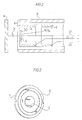
Fig. 2 zeigt eine bevorzugte Art der Anordnung der drei Elektroden S, R und E eines Näherungsschalters gemäß der Erfindung. Man erkennt, daß die Elektrode R, welche zusammen mit der plattenförmigen Sensorelektrode S die Stabilisierungskapazität Cs bildet, als - in der Praxis relativ kurze - zylinderförmige Ringelektrode ausgebildet ist, die unmittelbar hinter der Sensorelektrode S innerhalb des Gehäuses G angeordnet ist, und mit ihrem vorderen - in Fig. 2 linken - die Sensorelektrode S umgibt. In axialer Richtung hinter der Elektrode R ist die Elektrode E angeordnet, welche ebenfalls als zylindrische Ringelektrode ausgebildet ist und zusammen mit der Sensorelektrode S die Koppelkapazität Ck für das Einkoppeln der Prüfimpulse bildet. Die Anschlußleitungen für die Elektroden S, R und E sind in Fig. 2 mit den Bezugszeichen L1, L2 bzw. L3 bezeichnet. Die entsprechenden Leitungen sind in Fig. 1 mit denselben Bezugszeichen bezeichnet, wobei für die zur Basis des Transistors T1 führende Leitung L1 in üblicher Weise eine Abschirmung angedeutet ist.2 shows a preferred type of arrangement of the three electrodes S, R and E of a proximity switch according to the invention. It can be seen that the electrode R, which forms the stabilizing capacitance Cs together with the plate-shaped sensor electrode S, is designed as a - in practice relatively short - cylindrical ring electrode which is arranged directly behind the sensor electrode S within the housing G, and with its front one - In Fig. 2 left - surrounds the sensor electrode S. In the axial direction behind the electrode R, the electrode E is arranged, which is also designed as a cylindrical ring electrode and, together with the sensor electrode S, forms the coupling capacitance Ck for coupling the test pulses. The connecting lines for the electrodes S, R and E are designated in FIG. 2 by the reference symbols L1, L2 and L3. The corresponding lines are designated in FIG. 1 with the same reference symbols, a shield being indicated in the usual way for the line L1 leading to the base of the transistor T1.
In weiterer Ausgestaltung der Erfindung besteht gemäß Fig. 3 der Zeichnung die Möglichkeit, die Sensorelektrode S und die weitere Elektrode E an einem gemeinsamen plattenförmigen Träger T anzubringen. Typischerweise besteht der Träger T aus dem üblichen Leiterplattenmaterial, welches auf seiner einen Seite zunächst mit einer durchgehenden Metallschicht versehen ist, aus der dann durch Ätzen unter Anwendung der üblichen Photoätztechnik die Sensorelektrode S und die weitere Elektrode E herausgearbeitet werden. Wenn die Prüfimpulse direkt an das Gehäuse angelegt werden, dann kann in entsprechender Weise auch die zu der Stabilisierungskapazität Cs gehörende Elektrode R gemeinsam mit der Sensorelektrode S auf einem einzigen Träger T ausgebildet werden.In a further embodiment of the invention, according to FIG. 3 of the drawing, there is the possibility of attaching the sensor electrode S and the further electrode E to a common plate-shaped carrier T. Typically, the carrier T consists of the usual printed circuit board material, which is first provided on one side with a continuous metal layer, from which the sensor electrode S and the further electrode E are then worked out by etching using the customary photoetching technique. If the test pulses are applied directly to the housing, then the electrode R belonging to the stabilizing capacitance Cs can be formed in a corresponding manner together with the sensor electrode S on a single carrier T.
Aus der vorstehenden Beschreibung wird deutlich, daß erfindungsgemäß eine hohe Fehlersicherheit des Näherungsschalters erreichbar ist, da die Überwachung unmittelbar am Schaltereingang bzw. an der Sensorelektrode beginnt, wobei nicht nur die einwandfreie Funktion des Oszillatorverstärkers bzw. des Oszillatortransistors mit überwacht wird, sondern auch noch die einwandfreie Verbindung zwischen der Sensorelektrode und dem Steuereingang des Verstärkers. Weiterhin wird aus der Beschreibung deutlich, daß für die körperliche Realisierung der verschiedenen Elektroden eine Reihe von Möglichkeiten besteht, wobei speziell die konzentrische Elektrodenanordnung auf einer Leiterplatte besonders einfach und preiswert realisiert werden kann.From the above description it is clear that, according to the invention, a high level of error resistance of the proximity switch can be achieved, since the monitoring begins directly at the switch input or at the sensor electrode, not only the proper functioning of the oscillator amplifier or the oscillator transistor being monitored, but also that perfect connection between the sensor electrode and the control input of the amplifier. Furthermore, it is clear from the description that there are a number of options for the physical implementation of the various electrodes, in particular the concentric electrode arrangement on a printed circuit board can be implemented particularly simply and inexpensively.
Claims (8)
Applications Claiming Priority (2)
| Application Number | Priority Date | Filing Date | Title |
|---|---|---|---|
| DE3815698A DE3815698A1 (en) | 1988-05-07 | 1988-05-07 | SELF-TESTING, CAPACITIVE PROXIMITY SWITCH |
| DE3815698 | 1988-05-07 |
Publications (3)
| Publication Number | Publication Date |
|---|---|
| EP0341576A2 true EP0341576A2 (en) | 1989-11-15 |
| EP0341576A3 EP0341576A3 (en) | 1990-12-19 |
| EP0341576B1 EP0341576B1 (en) | 1995-06-28 |
Family
ID=6353920
Family Applications (1)
| Application Number | Title | Priority Date | Filing Date |
|---|---|---|---|
| EP89108068A Expired - Lifetime EP0341576B1 (en) | 1988-05-07 | 1989-05-04 | Self-checking capacitive proximity switch |
Country Status (2)
| Country | Link |
|---|---|
| EP (1) | EP0341576B1 (en) |
| DE (2) | DE3815698A1 (en) |
Cited By (8)
| Publication number | Priority date | Publication date | Assignee | Title |
|---|---|---|---|---|
| EP0515266A1 (en) * | 1991-05-23 | 1992-11-25 | Application Securite Positive Asept S.A. | Proximity detector for aerial power lines |
| EP0899882A1 (en) * | 1997-06-26 | 1999-03-03 | captron electronic gmbh | Circuit arrangement for a capacitive switch |
| DE19812626A1 (en) * | 1998-03-23 | 1999-09-30 | Bayerische Motoren Werke Ag | Capacitive object detection method for vehicles |
| EP0969600A1 (en) * | 1998-07-03 | 2000-01-05 | Siemens Aktiengesellschaft | Proximity switch with integral function testing |
| EP0996228A1 (en) * | 1998-10-22 | 2000-04-26 | Amphitech Société à responsabilité limitée | Touch sensitive switch |
| US6376939B1 (en) | 1999-04-02 | 2002-04-23 | Sumitomo Chemical Company, Limited | Sensor apparatus and safety apparatus for protecting approach to machines |
| DE102013201704A1 (en) * | 2013-02-01 | 2014-08-07 | Di-Soric Gmbh & Co. Kg | Capacitive sensor arrangement and capacitive measuring method with compensation of parasitic capacitances |
| WO2018089897A1 (en) * | 2016-11-14 | 2018-05-17 | Touchsensor Technologies, Llc | Capacitive sensor with self-test feature |
Families Citing this family (9)
| Publication number | Priority date | Publication date | Assignee | Title |
|---|---|---|---|---|
| DE4041550C3 (en) * | 1990-12-22 | 2003-08-28 | Schmersal K A Gmbh & Co | Safety device with at least one non-contact sensor |
| DE19623969B4 (en) * | 1996-06-15 | 2007-04-19 | Werner Turck Gmbh & Co. Kg | proximity switch |
| DE10206968A1 (en) * | 2002-02-19 | 2003-08-21 | Tegralis Gmbh | Method, for detecting operation of door or window handle, requires capacitive sensor with capacitance varied by operation of handle |
| DE10224537B8 (en) * | 2002-05-31 | 2006-01-12 | Fela Hilzinger Gmbh Leiterplattentechnik | Capacitive keyboard device and method for producing such a capacitive keyboard device |
| DE102004003112B4 (en) * | 2004-01-21 | 2005-12-22 | Dieter Peter | Device and method for capacitive measured value acquisition |
| DE102007025947B4 (en) | 2007-06-04 | 2009-02-26 | Fraunhofer-Gesellschaft zur Förderung der angewandten Forschung e.V. | Integrated capacitive sensor |
| DE102008044067A1 (en) * | 2008-11-25 | 2010-05-27 | Huf Hülsbeck & Fürst Gmbh & Co. Kg | Capacitive proximity sensor with a shield electrode and a diagnostic electrode |
| DE102012112248B4 (en) | 2012-12-13 | 2015-05-28 | Fela Holding Gmbh | Capacitive keyboard device with a preferably transparent front panel |
| DE102019112962A1 (en) | 2019-05-16 | 2020-11-19 | Karlsruher Institut für Technologie | Sensor module, system and method for operating the sensor module and system |
Citations (4)
| Publication number | Priority date | Publication date | Assignee | Title |
|---|---|---|---|---|
| DE2739786A1 (en) * | 1977-09-03 | 1979-03-15 | Turck Werner Kg | Capacitive proximity switch with two concentric electrodes - forms capacitor encircled by earthed screen electrode |
| EP0087094A1 (en) * | 1982-02-18 | 1983-08-31 | i f m electronic gmbh | Electronic circuit arrangement comprising a switching device and fault indicator |
| EP0132850A1 (en) * | 1983-07-28 | 1985-02-13 | Gebhard Balluff Fabrik feinmechanischer Erzeugnisse GmbH & Co. | Self-testing proximity switch |
| GB2177216A (en) * | 1985-07-05 | 1987-01-14 | Baumer Electric Ag | Proximity switch |
Family Cites Families (2)
| Publication number | Priority date | Publication date | Assignee | Title |
|---|---|---|---|---|
| DE2744785B2 (en) * | 1977-10-05 | 1981-05-21 | Robert 7995 Neukirch Buck | Electronic proximity switch |
| DE3150212C1 (en) * | 1981-12-18 | 1991-01-24 | Pepperl & Fuchs Gmbh & Co Kg, 6800 Mannheim | Circuit arrangement for a proximity switch |
-
1988
- 1988-05-07 DE DE3815698A patent/DE3815698A1/en not_active Ceased
-
1989
- 1989-05-04 EP EP89108068A patent/EP0341576B1/en not_active Expired - Lifetime
- 1989-05-04 DE DE58909315T patent/DE58909315D1/en not_active Expired - Fee Related
Patent Citations (4)
| Publication number | Priority date | Publication date | Assignee | Title |
|---|---|---|---|---|
| DE2739786A1 (en) * | 1977-09-03 | 1979-03-15 | Turck Werner Kg | Capacitive proximity switch with two concentric electrodes - forms capacitor encircled by earthed screen electrode |
| EP0087094A1 (en) * | 1982-02-18 | 1983-08-31 | i f m electronic gmbh | Electronic circuit arrangement comprising a switching device and fault indicator |
| EP0132850A1 (en) * | 1983-07-28 | 1985-02-13 | Gebhard Balluff Fabrik feinmechanischer Erzeugnisse GmbH & Co. | Self-testing proximity switch |
| GB2177216A (en) * | 1985-07-05 | 1987-01-14 | Baumer Electric Ag | Proximity switch |
Cited By (11)
| Publication number | Priority date | Publication date | Assignee | Title |
|---|---|---|---|---|
| EP0515266A1 (en) * | 1991-05-23 | 1992-11-25 | Application Securite Positive Asept S.A. | Proximity detector for aerial power lines |
| FR2676824A1 (en) * | 1991-05-23 | 1992-11-27 | Asept Applic Securite Positive | PROXIMITY DETECTOR FOR AERIAL ELECTRIC LINES. |
| EP0899882A1 (en) * | 1997-06-26 | 1999-03-03 | captron electronic gmbh | Circuit arrangement for a capacitive switch |
| DE19812626A1 (en) * | 1998-03-23 | 1999-09-30 | Bayerische Motoren Werke Ag | Capacitive object detection method for vehicles |
| EP0969600A1 (en) * | 1998-07-03 | 2000-01-05 | Siemens Aktiengesellschaft | Proximity switch with integral function testing |
| EP0996228A1 (en) * | 1998-10-22 | 2000-04-26 | Amphitech Société à responsabilité limitée | Touch sensitive switch |
| FR2785108A1 (en) * | 1998-10-22 | 2000-04-28 | Amphitech Sarl | SENSITIVE TOUCH CONTACTOR |
| US6376939B1 (en) | 1999-04-02 | 2002-04-23 | Sumitomo Chemical Company, Limited | Sensor apparatus and safety apparatus for protecting approach to machines |
| DE102013201704A1 (en) * | 2013-02-01 | 2014-08-07 | Di-Soric Gmbh & Co. Kg | Capacitive sensor arrangement and capacitive measuring method with compensation of parasitic capacitances |
| EP2763008A3 (en) * | 2013-02-01 | 2017-03-08 | Di-Soric GmbH & Co. KG, Urbach | Capacitative sensor assembly and capacitive measurement method with compensation of parasitic capacities |
| WO2018089897A1 (en) * | 2016-11-14 | 2018-05-17 | Touchsensor Technologies, Llc | Capacitive sensor with self-test feature |
Also Published As
| Publication number | Publication date |
|---|---|
| DE3815698A1 (en) | 1989-11-16 |
| EP0341576A3 (en) | 1990-12-19 |
| EP0341576B1 (en) | 1995-06-28 |
| DE58909315D1 (en) | 1995-08-03 |
Similar Documents
| Publication | Publication Date | Title |
|---|---|---|
| EP0341576B1 (en) | Self-checking capacitive proximity switch | |
| DE3220068C2 (en) | ||
| EP0228019B1 (en) | Proximity switch operating without contact | |
| DE2411810C3 (en) | Device for synchronizing droplet formation with droplet charging in an ink jet pen | |
| EP0213283A1 (en) | Coin testing apparatus | |
| EP0900997A1 (en) | Inductive angle sensor | |
| DE2726648C2 (en) | ||
| DE2448950A1 (en) | DEVICE FOR MEASURING POSITIONAL CHANGES | |
| DE3016821C2 (en) | Electronic proximity switch | |
| DE2904861B2 (en) | Piezoelectric liquid atomizer | |
| DE10143900A1 (en) | Inductive proximity sensor | |
| EP0171121A2 (en) | Data input keyboard with galvanic contacting keys | |
| DE3327188A1 (en) | SELF-TESTING PROXIMITY SWITCH | |
| DE2137893C3 (en) | Proximity signaling device | |
| WO1989008952A1 (en) | Anti-jamming device | |
| DE2448604A1 (en) | ELECTRONIC SWITCHING DEVICE | |
| DE2641744C2 (en) | Color jet recording device | |
| DE3206786A1 (en) | SHAKER DETECTOR FOR A RING LASER GYROSCOPE | |
| DE2140056C3 (en) | Contactless controllable proximity switch | |
| DE2413761A1 (en) | CAPACITIVE PRESSURE TRANSDUCER OR FREQUENCY CONVERTER | |
| DE3034148A1 (en) | MONITORING CIRCUIT, IN PARTICULAR FOR THE TIRE PRESSURE OF MOTOR VEHICLES | |
| DE2647569C3 (en) | Pulse generator with switchable output frequency | |
| DE2452732C3 (en) | Device for determining whether a switch provided as a transducer is in the open or closed state | |
| DE2745650C2 (en) | Proximity switch | |
| DE3612182C2 (en) | RC oscillator |
Legal Events
| Date | Code | Title | Description |
|---|---|---|---|
| PUAI | Public reference made under article 153(3) epc to a published international application that has entered the european phase |
Free format text: ORIGINAL CODE: 0009012 |
|
| AK | Designated contracting states |
Kind code of ref document: A2 Designated state(s): CH DE IT LI |
|
| PUAL | Search report despatched |
Free format text: ORIGINAL CODE: 0009013 |
|
| AK | Designated contracting states |
Kind code of ref document: A3 Designated state(s): CH DE IT LI |
|
| 17P | Request for examination filed |
Effective date: 19910618 |
|
| 17Q | First examination report despatched |
Effective date: 19930527 |
|
| GRAA | (expected) grant |
Free format text: ORIGINAL CODE: 0009210 |
|
| AK | Designated contracting states |
Kind code of ref document: B1 Designated state(s): CH DE IT LI |
|
| ITF | It: translation for a ep patent filed |
Owner name: BARZANO' E ZANARDO MILANO S.P.A. |
|
| REF | Corresponds to: |
Ref document number: 58909315 Country of ref document: DE Date of ref document: 19950803 |
|
| PLBE | No opposition filed within time limit |
Free format text: ORIGINAL CODE: 0009261 |
|
| STAA | Information on the status of an ep patent application or granted ep patent |
Free format text: STATUS: NO OPPOSITION FILED WITHIN TIME LIMIT |
|
| PG25 | Lapsed in a contracting state [announced via postgrant information from national office to epo] |
Ref country code: LI Effective date: 19960531 Ref country code: CH Effective date: 19960531 |
|
| 26N | No opposition filed | ||
| REG | Reference to a national code |
Ref country code: CH Ref legal event code: PL |
|
| PGFP | Annual fee paid to national office [announced via postgrant information from national office to epo] |
Ref country code: DE Payment date: 19980625 Year of fee payment: 10 |
|
| PG25 | Lapsed in a contracting state [announced via postgrant information from national office to epo] |
Ref country code: DE Free format text: LAPSE BECAUSE OF NON-PAYMENT OF DUE FEES Effective date: 20000301 |
|
| PG25 | Lapsed in a contracting state [announced via postgrant information from national office to epo] |
Ref country code: IT Free format text: LAPSE BECAUSE OF NON-PAYMENT OF DUE FEES Effective date: 20050504 |