EP0337463A2 - Emulationssystem, fähig zur Anpassung an Mikrorechner mit verschiedenen On-Chip-Speicherkapazitäten - Google Patents
Emulationssystem, fähig zur Anpassung an Mikrorechner mit verschiedenen On-Chip-Speicherkapazitäten Download PDFInfo
- Publication number
- EP0337463A2 EP0337463A2 EP89106639A EP89106639A EP0337463A2 EP 0337463 A2 EP0337463 A2 EP 0337463A2 EP 89106639 A EP89106639 A EP 89106639A EP 89106639 A EP89106639 A EP 89106639A EP 0337463 A2 EP0337463 A2 EP 0337463A2
- Authority
- EP
- European Patent Office
- Prior art keywords
- chip
- memory
- address
- evaluation chip
- area
- Prior art date
- Legal status (The legal status is an assumption and is not a legal conclusion. Google has not performed a legal analysis and makes no representation as to the accuracy of the status listed.)
- Granted
Links
Images


Classifications
-
- G—PHYSICS
- G06—COMPUTING OR CALCULATING; COUNTING
- G06F—ELECTRIC DIGITAL DATA PROCESSING
- G06F9/00—Arrangements for program control, e.g. control units
- G06F9/06—Arrangements for program control, e.g. control units using stored programs, i.e. using an internal store of processing equipment to receive or retain programs
- G06F9/44—Arrangements for executing specific programs
- G06F9/455—Emulation; Interpretation; Software simulation, e.g. virtualisation or emulation of application or operating system execution engines
- G06F9/45533—Hypervisors; Virtual machine monitors
- G06F9/45537—Provision of facilities of other operating environments, e.g. WINE
Definitions
- the present invention relates to an emulation system for microcomputers.
- emulation systems are indispensable to development of programs for different microcomputers.
- the conventional emulation system are constructed under the assumption that a target microcomputer to be emulated has an on-chip memory area of a fixed capacity, for example 256 bytes, and a memory area exceeding 256 bytes is provided as an external memory. Therefore, if a target microcomputer chip having an on-chip memory area of for example 512 bytes is emulated, a first half of the 512 bytes is accessed as an on-chip memory access, but a second half of the 512 bytes is accessed as an external memory access. In other words, the second half of the 512 bytes cannot be properly emulated as the on-chip memory access.
- Another object of the present invention is to provide an emulation system capable of emulating an access to an on-chip memory of a target microcomputer having even a large memory capacity, with the access speed of the target microcomputer.
- an emulation system which includes an evaluation chip, a program memory and a data memory and is coupled to an external memory, comprising means for discriminating whether or not a space to be accessed by the evaluation chip is within an on-chip area of a target microcomputer and notifying the result of discrimination to the evaluation chip, so that the evaluation chip operates to access the data memory when the space to be accessed by the evaluation chip is within the on-chip area of the target microcomputer and the external memory when the space to be accessed by the evaluation chip is not within the on-chip area of the target microcomputer.
- the size or scale of the on-chip memory area is not set within the evaluation chip, but the discriminating means discriminates whether or not the space to be accessed by the evaluation chip is within the on-chip memory area of the target microcomputer, and the result of discrimination is notified to the evaluation chip.
- This discrimination can be performed, for example, by decoding an address outputted from the evaluation chip. Therefore, the size or scale which should be deemed as the on-chip memory area can be freely set in the discriminating means, and accordingly, the emulation chip can emulate various target memories having different on-chip memory capacities.
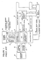
- FIG. 1 there is shown a diagram of one example of the conventional emulation system, which can access to an external memory and is able to emulate a microcomputer having an on-chip memory therein.
- the shown emulation system comprises an evaluation chip 10 which includes therein a central processing unit (called “CPU” hereinafter) 12, an external bus interface 14 and a data memory interface 16.
- the evaluation chip 10 is coupled to a program memory 20 storing a program therein, through a program address bus 22 which is used for supplying a program address from the evaluation chip 10 to the program memory 20 and through a program data bus 24 which is used for supplying a program read from the program memory 20 to the evaluation chip 10.
- the evaluation chip 10 is coupled to a data memory 30 through a memory address bus 32 which is used for supplying a memory address from the evaluation chip 10 to the data memory 20 and through a memory data bus 34 which is used for transferring data between the data memory 30 and the CPU 12 of the evaluation chip 10.
- the evaluation chip 10 generates a memory write signal 36 and a memory read signal 38 to the data memory 30.
- a high order or place address latch 40 which has an input coupled to the memory address bus 32 for temporarily latching a high place portion of an address supplied onto the memory address bus 32.
- This latch 40 is connected to receive a high place address latch enable signal 42 from the evaluation chip 10, and has an output coupled to the data memory 30 for supplying the latched high place address to the data memory 30.
- the evaluation chip 10 is coupled to an external memory 50 through an external address bus 52 which is used for supplying a memory address from the evaluation chip 10 to the external memory 50 and through an external data bus 54 which is used for transferring data between the external memory 50 and the CPU 12 of the evaluation chip 10.
- the evaluation chip 10 generates an external memory write signal 56 and an external memory read signal 58 to the external memory 50.
- the CPU 12 fetches an instruction from the program memory 20 and the result of the instruction decoding indicates that data "96 H " should be written to an address "FE5A H ", since the high place portion of the address is "FE H ", the CPU judges that the data should be written to the on-chip memory area and then starts a necessary write operation.
- FIG. 2 there is illustrated a timing chart of the operation of the emulation system in the case of accessing to the on-chip memory area.
- the CPU 12 outputs the high place address "FE H " to the memory address bus 32, and at the same time, activates the high place address latch enable signal 42, so that the high place address "FE H " is latched to the high place address latch 40 in a state T1 shown in Figure 2.
- the latch 40 supplies the high place address "FE H " to the data memory 30.
- the CPU 12 outputs a lower place address "5A H " to the memory address bus 32, and at the same time, outputs the data "96 H " to the memory data bus 34 and activates the memory write signal 36.
- the data "96 H” is written from the CPU 12 to the address "FE5A H " of the data memory 30 (state T2).
- a read operation can be executed similarly to the above mentioned write operation, except that the memory read signal 38 is activated in place of the memory write signal 36 and the CPU 12 fetches data read out onto the memory data bus 34 from the memory 30.
- the CPU 12 fetches an instruction from the program memory 20 and the result of the instruction decoding indicates that data "96 H " should be written to an address "FD5A H " which does not exist within the on-chip memory area, the CPU judges that the data should be written to a memory area other than the on-chip memory area. In this case, the CPU 12 access through an external bus interface 14 to the memory 50 external to the emulation system. Five system clocks are required for this access.
- Figure 3 is a timing chart illustrating the operation of the conventional emulation system in the case of accessing to the external memory.
- the CPU 12 outputs the high place address "FD H " to the external address bus 52 in a state T1 shown in Figure 3.
- the CPU 12 outputs the lower place address "5A H “ to the external address bus 52, and at the same time, outputs the data "96 H “ to the external data bus 54 and activates the external write signal 56.
- the data "96 H " is written from the CPU 12 to the address "FD5A H " of the memory area other than the on-chip memory area (state T2).
- the state T2 for the external access is composed of four system clocks.
- a read operation can be executed similarly to the above mentioned write operation, except that the external read signal 58 is activated in place of the external write signal 56 and the CPU 12 fetches data read out onto the external data bus 34 from the external.
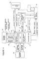
- Figure 4 is a block diagram of a first embodiment of the emulation system in accordance with the present invention.
- Figure 5 is a timing chart illustrating the operation of the emulation system in the case of accessing to the on-chip memory area
- Figure 6 is a timing chart illustrating the operation of the emulation system in the case of accessing to the external memory.
- Figure 7 is a memory map illustrating an on-chip memory area area of 256 bytes
- Figure 8 is a memory map illustrating an on-chip memory area of 512 bytes.
- the first embodiment of the emulation system in accordance with the present invention additionally comprises an area discriminater 60, which is in turn coupled to the memory address bus 32 and connected to receive the high place address latch enable signal 42, and which generates an area designation signal 62 to the evaluation chip 10.
- the area discriminater fetches the high place address on the memory address bus 32, and discriminates whether or not the address to be accessed is within the on-chip memory area.
- the area discriminater 60 activates the ares designation signal 60 so as to notify the CPU 12 that the address to be accessed is within the on-chip memory area. On the other hand, if the address to be accessed is not within the on-chip memory area, the area discriminater 60 does not activate the ares designation signal 60. Since the area discriminater 60 discriminates whether or not the address to be accessed is within the on-chip memory area, it is possible to freely set or designate an address extent assigned to the on-chip memory area. In other words, it is possible to freely determine a first address and a last address of the on-chip memory area. In this embodiment, the CPU 12 requires two system clocks for access to the on-chip memory area but five system clocks for access to memory areas other than the on-chip memory area.
- the CPU 12 fetches an instruction from the program memory 20 and the result of the instruction decoding indicates that data "96 H " should be written to an address "FE5A H ", the CPU 12 performs a necessary write operation in the sequence as shown in Figure 5 which illustrates a timing chart of the operation of the emulation system in the case of accessing to the on-chip memory area.
- the CPU 12 outputs the high place address "FE H " to the memory address bus 32 and the external address bus 52, and at the same time, activates the high place address latch enable signal 42, so that the high place address "FE H " is latched to the high place address latch 40 in a state T1 shown in Figure 2.
- the area discriminater 60 discriminates whether or not the address "FE H " on the memory address bus 32 is within a space assigned to the on-chip memory area. In this case, since the address "FE H " is within the space assigned to the on-chip memory area area, the area discriminater 60 activates the area designation signal 62, and in response to the activated designation signal 62, the CPU 12 judges that the access is directed to the on-chip memory area (state T1).
- the CPU 12 outputs a lower place address "5A H " to the memory address bus 32, and at the same time, outputs the data "96 H “ to the memory data bus 34 and also activates the memory write signal 36.
- the CPU executes the access of two system clocks.
- the data "96 H " is written from the CPU 12 to the address "FE5A H " of the data memory 30 (state T2) as the access to the on-chip memory area.
- a read operation can be executed similarly to the above mentioned write operation, except that the memory read signal 38 is activated in place of the memory write signal 36 and the CPU 12 fetches data read out on the memory data bus 34 from the memory 30.
- the CPU 12 fetches an instruction from the program memory 20 and the result of the instruction decoding indicates that data "96 H " should be written to an address "FD5A H " which does not exist within the on-chip memory area, the CPU 12 starts a necessary write operation in the sequence as shown in Figure 6 which illustrates a timing chart of the operation of the emulation system in the case of accessing to the external memory area.
- the CPU 12 outputs the high place address "FD H " to the memory address bus 32 and the external address bus 52 in a state T1 shown in Figure 6.
- the CPU activates the high place address latch enable signal 42.
- the area discriminater 60 discriminates whether or not the address "FD H " on the memory address bus 32 is within a space assigned to the on-chip memory area. In this case, since the address "FD H " is not within a space assigned to the on-chip memory area, the area discriminater 60 does not activates the area designation signal 62. As a result, the CPU 12 judges that the access is not directed to the on-chip memory area (state T1).
- the CPU 12 outputs the lower place address "5A H " to the external address bus 52, and at the same time, outputs the data "96 H “ to the external data bus 54 and activates the external write signal 56.
- the data "96 H " is written from the CPU 12 through the external bus interface 14 to the address "FD5A H " of the memory area (the external memory 50) other than the on-chip memory area (state T2).
- the state T2 is composed of four system clocks.
- a read operation can be executed similarly to the above mentioned write operation, except that the external read signal 58 is activated in place of the external write signal 56 and the CPU 12 fetches data read out onto the external data bus 34 from the external.
- the CPU 12 fetches an instruction from the program memory 20 and the result of the instruction decoding indicates that data "96 H " should be written to an address "FD5A H ", the CPU starts a necessary write operation in the sequence as mentioned below.
- the CPU 12 outputs the high place address "FD H ", to the memory address bus 32 and the external address bus 52, and at the same time, activates the high place address latch enable signal 42.
- the area discriminater 60 discriminates whether or not the address "FD H " on the memory address bus 32 is within a space assigned to the on-chip memory area.
- the area discriminater 60 activates the area designation signal 62.
- the CPU 12 write the data "96 H " to the address "FD5A H " as the access to the on-chip memory area, similarly to the above mentioned on-chip memory area writing operation in the case that the capacity of the on-chip memory area is set to 256 bytes.
- FIG. 9 there is shown a block diagram of a second embodiment of the emulation system in accordance with the present invention.
- elements similar or corresponding to those shown in Figure 4 are given the same Reference Numerals, and explanation thereof will be omitted.
- the second embodiment shown in Figure 9 additionally includes a second data memory 30A, which is in turn coupled to the memory address bus 32, the memory data bus 34 and the high place address latch 40 and also connected to receive the memory write signal 36 and the memory read signal 38.
- the second data memory 30A is provided for emulating the target microcomputer, similarly to the first data memory 30, but is different from the first data memory 30 in the number of required access cycles.
- the area discriminater 60 generates not only the area designation signal 62 but also a second designation signal 62A. Both of the first and second designation signals 62 and 62A indicate whether or not the address to be accessed is within the on-chip memory area. However, the area designation signal 62 designates the first data memory 30 and the second designation signal 62A indicates the second data memory 30A.
- the area discriminater 60 is set to activate the first area designation signal 62 when the CPU accesses any of the addresses "FE00 H “ to FEFF H " and the second area designation signal 62A when the CPU accesses any of the addresses "FC00 H “ to "FCFF H ".
- the second embodiment can emulate the target microcomputer with the proper numbers of access cycles.
- the evaluation chip (the CPU) does not determine whether or not the access space is within the on-chip memory area.
- the area discriminater receives a high place address of the address which is supplied from the evaluation chip, and discriminates whether or not the space to be accessed by the evaluation chip is within the on-chip memory area. In addition, the area discriminater notifies the result of discrimination to the evaluation chip to cause the evaluation chip to execute an access operation with reference to the result of discrimination. Accordingly, it is possible to emulate various target microcomputers having different on-chip memory area capacities, with respective proper access cycles.
Landscapes
- Engineering & Computer Science (AREA)
- Software Systems (AREA)
- Theoretical Computer Science (AREA)
- Physics & Mathematics (AREA)
- General Engineering & Computer Science (AREA)
- General Physics & Mathematics (AREA)
- Test And Diagnosis Of Digital Computers (AREA)
- Multi Processors (AREA)
- Memory System (AREA)
- Microcomputers (AREA)
Applications Claiming Priority (2)
| Application Number | Priority Date | Filing Date | Title |
|---|---|---|---|
| JP92076/88 | 1988-04-13 | ||
| JP63092076A JPH0724029B2 (ja) | 1988-04-13 | 1988-04-13 | エミュレーション装置 |
Publications (3)
| Publication Number | Publication Date |
|---|---|
| EP0337463A2 true EP0337463A2 (de) | 1989-10-18 |
| EP0337463A3 EP0337463A3 (de) | 1991-08-07 |
| EP0337463B1 EP0337463B1 (de) | 1996-10-09 |
Family
ID=14044361
Family Applications (1)
| Application Number | Title | Priority Date | Filing Date |
|---|---|---|---|
| EP89106639A Expired - Lifetime EP0337463B1 (de) | 1988-04-13 | 1989-04-13 | Emulationssystem, fähig zur Anpassung an Mikrorechner mit verschiedenen On-Chip-Speicherkapazitäten |
Country Status (4)
| Country | Link |
|---|---|
| US (1) | US5168559A (de) |
| EP (1) | EP0337463B1 (de) |
| JP (1) | JPH0724029B2 (de) |
| DE (1) | DE68927306T2 (de) |
Cited By (3)
| Publication number | Priority date | Publication date | Assignee | Title |
|---|---|---|---|---|
| US6785886B1 (en) | 1998-05-15 | 2004-08-31 | Vmware, Inc. | Deferred shadowing of segment descriptors in a virtual machine monitor for a segmented computer architecture |
| US7516453B1 (en) | 1998-10-26 | 2009-04-07 | Vmware, Inc. | Binary translator with precise exception synchronization mechanism |
| US8631066B2 (en) | 1998-09-10 | 2014-01-14 | Vmware, Inc. | Mechanism for providing virtual machines for use by multiple users |
Families Citing this family (11)
| Publication number | Priority date | Publication date | Assignee | Title |
|---|---|---|---|---|
| JPH0476681A (ja) * | 1990-07-13 | 1992-03-11 | Mitsubishi Electric Corp | マイクロコンピュータ |
| JPH04177543A (ja) * | 1990-11-09 | 1992-06-24 | Nec Ic Microcomput Syst Ltd | マイクロコンピュータ |
| JP2856591B2 (ja) * | 1991-06-27 | 1999-02-10 | 三菱電機株式会社 | マイクロコンピュータ、プログラム開発装置およびプログラム開発システム |
| JPH05257710A (ja) * | 1991-08-12 | 1993-10-08 | Advanced Micro Devicds Inc | 内部実行パラメータを与えるためのシステムおよびプロセッサによって実行されるべき命令を検証するための配列 |
| JPH0789340B2 (ja) * | 1992-01-02 | 1995-09-27 | インターナショナル・ビジネス・マシーンズ・コーポレイション | バス間インターフェースにおいてアドレス・ロケーションの判定を行なう方法及び装置 |
| FR2696561B1 (fr) * | 1992-10-02 | 1994-12-23 | Sgs Thomson Microelectronics | Micro-calculateur pouvant fonctionner en mode d'émulation avec des périphériques internes et externes. |
| US5557743A (en) * | 1994-04-05 | 1996-09-17 | Motorola, Inc. | Protection circuit for a microprocessor |
| US5737760A (en) * | 1995-10-06 | 1998-04-07 | Motorola Inc. | Microcontroller with security logic circuit which prevents reading of internal memory by external program |
| JP4312272B2 (ja) * | 1995-10-06 | 2009-08-12 | モトローラ・インコーポレイテッド | 内部メモリへのアクセスを制限するマイクロコントローラ |
| JP3620181B2 (ja) * | 1996-12-05 | 2005-02-16 | 富士通株式会社 | 半導体装置及びリードアクセス方法 |
| CA2251295C (en) * | 1998-01-27 | 2002-08-20 | Sharp Kabushiki Kaisha | Electric vacuum cleaner |
Family Cites Families (6)
| Publication number | Priority date | Publication date | Assignee | Title |
|---|---|---|---|---|
| US3972025A (en) * | 1974-09-04 | 1976-07-27 | Burroughs Corporation | Expanded memory paging for a programmable microprocessor |
| US4450519A (en) * | 1980-11-24 | 1984-05-22 | Texas Instruments Incorporated | Psuedo-microprogramming in microprocessor in single-chip microprocessor with alternate IR loading from internal or external program memories |
| US4434462A (en) * | 1980-11-24 | 1984-02-28 | Texas Instruments Incorporated | Off-chip access for psuedo-microprogramming in microprocessor |
| US4450524A (en) * | 1981-09-23 | 1984-05-22 | Rca Corporation | Single chip microcomputer with external decoder and memory and internal logic for disabling the ROM and relocating the RAM |
| IT1142074B (it) * | 1981-11-24 | 1986-10-08 | Honeywell Inf Systems | Sistema di elaborazione dati con allocazione automatica dell'indirizzo in una memoria modulare |
| US4514805A (en) * | 1982-02-22 | 1985-04-30 | Texas Instruments Incorporated | Interrupt operation in systems emulator mode for microcomputer |
-
1988
- 1988-04-13 JP JP63092076A patent/JPH0724029B2/ja not_active Expired - Fee Related
-
1989
- 1989-04-13 US US07/337,756 patent/US5168559A/en not_active Expired - Lifetime
- 1989-04-13 EP EP89106639A patent/EP0337463B1/de not_active Expired - Lifetime
- 1989-04-13 DE DE68927306T patent/DE68927306T2/de not_active Expired - Fee Related
Cited By (5)
| Publication number | Priority date | Publication date | Assignee | Title |
|---|---|---|---|---|
| US6785886B1 (en) | 1998-05-15 | 2004-08-31 | Vmware, Inc. | Deferred shadowing of segment descriptors in a virtual machine monitor for a segmented computer architecture |
| US8631066B2 (en) | 1998-09-10 | 2014-01-14 | Vmware, Inc. | Mechanism for providing virtual machines for use by multiple users |
| US9323550B2 (en) | 1998-09-10 | 2016-04-26 | Vmware, Inc. | Mechanism for providing virtual machines for use by multiple users |
| US7516453B1 (en) | 1998-10-26 | 2009-04-07 | Vmware, Inc. | Binary translator with precise exception synchronization mechanism |
| US8296551B2 (en) | 1998-10-26 | 2012-10-23 | Vmware, Inc. | Binary translator with precise exception synchronization mechanism |
Also Published As
| Publication number | Publication date |
|---|---|
| EP0337463A3 (de) | 1991-08-07 |
| JPH01263737A (ja) | 1989-10-20 |
| DE68927306D1 (de) | 1996-11-14 |
| EP0337463B1 (de) | 1996-10-09 |
| US5168559A (en) | 1992-12-01 |
| JPH0724029B2 (ja) | 1995-03-15 |
| DE68927306T2 (de) | 1997-05-07 |
Similar Documents
| Publication | Publication Date | Title |
|---|---|---|
| US5664199A (en) | Microcomputer free from control of central processing unit (CPU) for receiving and writing instructions into memory independent of and during execution of CPU | |
| EP1196842B1 (de) | Vorrichtung und verfahren zum kombinieren von mehreren speicherzugrifftransaktionen | |
| US5168559A (en) | Emulation system capable of complying with microcomputers having different on-chip memory capacities | |
| US5784625A (en) | Method and apparatus for effecting a soft reset in a processor device without requiring a dedicated external pin | |
| US5862148A (en) | Microcontroller with improved debug capability for internal memory | |
| US6687811B1 (en) | Processor with trace memory for storing access information on internal bus | |
| US6401197B1 (en) | Microprocessor and multiprocessor system | |
| US6226736B1 (en) | Microprocessor configuration arrangement for selecting an external bus width | |
| US5832251A (en) | Emulation device | |
| US5903912A (en) | Microcontroller configured to convey data corresponding to internal memory accesses externally | |
| EP0757316B1 (de) | Auswahleinheit für externe Geräte in einem Datenprozessor | |
| US6742142B2 (en) | Emulator, a data processing system including an emulator, and method of emulation for testing a system | |
| US5155838A (en) | Computer system with emulation mechanism | |
| US7080191B2 (en) | Method and system for accessing memory devices | |
| US4814977A (en) | Apparatus and method for direct memory to peripheral and peripheral to memory data transfers | |
| KR20030055150A (ko) | 마이크로프로세서 및 마이크로프로세서의 처리 방법 | |
| EP0463352B1 (de) | Schaltungsinnerer Emulatormikroprozessor mit getrenntem Nutzer- und Schaltungsinnerem Emulatorspeicher | |
| US4628450A (en) | Data processing system having a local memory which does not use a directory device with distributed resident programs and a method therefor | |
| EP0795827A1 (de) | Speicheranordnung und Verfahren zum Zugreifen auf die Speicher der Speicheranordnung | |
| EP0117837B1 (de) | Benutzerprogrammierbare Buskonfiguration für Mikrocomputer | |
| CN1004945B (zh) | 地址控制装置 | |
| US6742073B1 (en) | Bus controller technique to control N buses | |
| JPS6255733A (ja) | 制御記憶装置 | |
| EP0328422A2 (de) | Mikrokomputersystem | |
| JPS6320545A (ja) | エミユレ−タのレジスタ読出し装置 |
Legal Events
| Date | Code | Title | Description |
|---|---|---|---|
| PUAI | Public reference made under article 153(3) epc to a published international application that has entered the european phase |
Free format text: ORIGINAL CODE: 0009012 |
|
| 17P | Request for examination filed |
Effective date: 19890413 |
|
| AK | Designated contracting states |
Kind code of ref document: A2 Designated state(s): DE FR GB IT |
|
| PUAL | Search report despatched |
Free format text: ORIGINAL CODE: 0009013 |
|
| AK | Designated contracting states |
Kind code of ref document: A3 Designated state(s): DE FR GB IT |
|
| 17Q | First examination report despatched |
Effective date: 19930601 |
|
| GRAG | Despatch of communication of intention to grant |
Free format text: ORIGINAL CODE: EPIDOS AGRA |
|
| GRAH | Despatch of communication of intention to grant a patent |
Free format text: ORIGINAL CODE: EPIDOS IGRA |
|
| GRAH | Despatch of communication of intention to grant a patent |
Free format text: ORIGINAL CODE: EPIDOS IGRA |
|
| GRAA | (expected) grant |
Free format text: ORIGINAL CODE: 0009210 |
|
| AK | Designated contracting states |
Kind code of ref document: B1 Designated state(s): DE FR GB IT |
|
| REF | Corresponds to: |
Ref document number: 68927306 Country of ref document: DE Date of ref document: 19961114 |
|
| ET | Fr: translation filed | ||
| ITF | It: translation for a ep patent filed | ||
| PLBE | No opposition filed within time limit |
Free format text: ORIGINAL CODE: 0009261 |
|
| STAA | Information on the status of an ep patent application or granted ep patent |
Free format text: STATUS: NO OPPOSITION FILED WITHIN TIME LIMIT |
|
| 26N | No opposition filed | ||
| REG | Reference to a national code |
Ref country code: GB Ref legal event code: IF02 |
|
| REG | Reference to a national code |
Ref country code: GB Ref legal event code: 732E |
|
| REG | Reference to a national code |
Ref country code: FR Ref legal event code: TP |
|
| PGFP | Annual fee paid to national office [announced via postgrant information from national office to epo] |
Ref country code: GB Payment date: 20040407 Year of fee payment: 16 |
|
| PGFP | Annual fee paid to national office [announced via postgrant information from national office to epo] |
Ref country code: FR Payment date: 20040408 Year of fee payment: 16 |
|
| PGFP | Annual fee paid to national office [announced via postgrant information from national office to epo] |
Ref country code: DE Payment date: 20040422 Year of fee payment: 16 |
|
| PG25 | Lapsed in a contracting state [announced via postgrant information from national office to epo] |
Ref country code: IT Free format text: LAPSE BECAUSE OF NON-PAYMENT OF DUE FEES;WARNING: LAPSES OF ITALIAN PATENTS WITH EFFECTIVE DATE BEFORE 2007 MAY HAVE OCCURRED AT ANY TIME BEFORE 2007. THE CORRECT EFFECTIVE DATE MAY BE DIFFERENT FROM THE ONE RECORDED. Effective date: 20050413 Ref country code: GB Free format text: LAPSE BECAUSE OF NON-PAYMENT OF DUE FEES Effective date: 20050413 |
|
| PG25 | Lapsed in a contracting state [announced via postgrant information from national office to epo] |
Ref country code: DE Free format text: LAPSE BECAUSE OF NON-PAYMENT OF DUE FEES Effective date: 20051101 |
|
| GBPC | Gb: european patent ceased through non-payment of renewal fee |
Effective date: 20050413 |
|
| PG25 | Lapsed in a contracting state [announced via postgrant information from national office to epo] |
Ref country code: FR Free format text: LAPSE BECAUSE OF NON-PAYMENT OF DUE FEES Effective date: 20051230 |
|
| REG | Reference to a national code |
Ref country code: FR Ref legal event code: ST Effective date: 20051230 |