EP0336951B1 - Integrated circuit contact fabrication process - Google Patents
Integrated circuit contact fabrication process Download PDFInfo
- Publication number
- EP0336951B1 EP0336951B1 EP88909410A EP88909410A EP0336951B1 EP 0336951 B1 EP0336951 B1 EP 0336951B1 EP 88909410 A EP88909410 A EP 88909410A EP 88909410 A EP88909410 A EP 88909410A EP 0336951 B1 EP0336951 B1 EP 0336951B1
- Authority
- EP
- European Patent Office
- Prior art keywords
- layer
- electrode layer
- refractory metal
- dielectric
- process according
- Prior art date
- Legal status (The legal status is an assumption and is not a legal conclusion. Google has not performed a legal analysis and makes no representation as to the accuracy of the status listed.)
- Expired - Lifetime
Links
Images




Classifications
-
- H—ELECTRICITY
- H10—SEMICONDUCTOR DEVICES; ELECTRIC SOLID-STATE DEVICES NOT OTHERWISE PROVIDED FOR
- H10D—INORGANIC ELECTRIC SEMICONDUCTOR DEVICES
- H10D44/00—Charge transfer devices
- H10D44/01—Manufacture or treatment
- H10D44/041—Manufacture or treatment having insulated gates
-
- H—ELECTRICITY
- H10—SEMICONDUCTOR DEVICES; ELECTRIC SOLID-STATE DEVICES NOT OTHERWISE PROVIDED FOR
- H10W—GENERIC PACKAGES, INTERCONNECTIONS, CONNECTORS OR OTHER CONSTRUCTIONAL DETAILS OF DEVICES COVERED BY CLASS H10
- H10W20/00—Interconnections in chips, wafers or substrates
- H10W20/01—Manufacture or treatment
- H10W20/031—Manufacture or treatment of conductive parts of the interconnections
- H10W20/064—Manufacture or treatment of conductive parts of the interconnections by modifying the conductivity of conductive parts, e.g. by alloying
- H10W20/066—Manufacture or treatment of conductive parts of the interconnections by modifying the conductivity of conductive parts, e.g. by alloying by forming silicides of refractory metals
-
- H—ELECTRICITY
- H10—SEMICONDUCTOR DEVICES; ELECTRIC SOLID-STATE DEVICES NOT OTHERWISE PROVIDED FOR
- H10W—GENERIC PACKAGES, INTERCONNECTIONS, CONNECTORS OR OTHER CONSTRUCTIONAL DETAILS OF DEVICES COVERED BY CLASS H10
- H10W20/00—Interconnections in chips, wafers or substrates
- H10W20/01—Manufacture or treatment
- H10W20/071—Manufacture or treatment of dielectric parts thereof
- H10W20/092—Manufacture or treatment of dielectric parts thereof by smoothing the dielectric parts
Definitions
- This invention relates to integrated circuit contact fabrication processes of the kind including the steps of: forming over an active region of a semiconductor substrate a first patterned electrode layer and an overlying first dielectric layer; forming in the active region and on said first dielectric layer a second electrode layer overlying at least an edge of said first electrode layer, to create a nonplanar step in the region of overlap with said first electrode layer; and forming a refractory metal based layer on said second electrode layer, said second electrode layer being patterned to retain the nonplanar step.
- FIG. l A process for integrated circuit contact fabrication is known from US-A-4,403,394 and is illustrated in Fig. l of the present drawings.
- the prior art represents a portion of a DRAM cell formed in a lightly doped p-type monocrystalline substrate l, having an n+ conductively doped region 2 on one side of the active region and a doped polycrystalline silicon layer 3 (poly I) situated at the other side.
- the active region is bordered on the sides by field oxides 4.
- Poly I layer 3 is one electrode of a capacitor, which is selectively coupled to conductive region 2 upon the enablement of the field effect transistor formed by secondly deposited polysilicon gate electrode 6 (poly II) through a channel between region 2 and the substrate proximate electrode 3.
- An oxide dielectric 7 covers electrode 6. Connections between the poly II electrode layer 6 and subsequent metalization layers are made by contacts using metal 8, formed in known manner by masking and then etching openings through dielectric 7, depositing of a metal layer, and patterning the metalization.
- the known process has the disadvantage that the concluding contour is far from planar, and that the extent of overlapping between poly I capacitor electrode 3 and poly II gate electrode 6 must be significant to ensure that alignment tolerances do not result in a contact cut down to the level of the poly I layer by a misalignment of the contact cut mask over the edge of poly II layer.
- a relatively large contact area between metal 8 and poly II electrode 6 is also required to minimize the effects of contact resistance on the conduction of charge to poly II electrode 6.
- the known process also has a disadvantage that the contact masking and etching steps are costly, and furthermore the area of the underlying polysilicon layer must be relatively large to compensate for alignment errors which are introduced by the successive masking operations.
- an integrated circuit contact fabrication process of the kind specified in the opening paragraph of this description, characterized by the steps of: planarizing the structure with second dielectric to selectively expose the surface of the refractory metal based layer; and forming a patterned metalization layer over the second dielectric to make contact with the exposed surface of the refractory metal based layer.
- an integrated circuit contact fabrication process has the advantage of providing a self-aligned contact structure and the further advantages of not requiring masking or etching to form contact openings in a dielectric layer, reducing the polysilicon area allocation for mask alignment tolerances, minimizing metal step coverage problems, providing low ohmic resistance contact connections, and providing a degree of planarization for subsequent metalization layers.
- the use of a contact fabrication process according to the invention reduces the "footprint" or area of the contact from the metalization layer to the second polysilicon gate electrode, and thereby measurably reduces undesired capacitive coupling between the gate electrode of the access transistor and the storage capacitor electrode.
- Fig. l is a cross-sectional schematic of a DRAM fabricated according to the prior art.
- Figs. 2 and 3 illustrate by way of schematic cross sections two embodiments of DRAM cells fabricated according to the present invention.
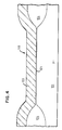
- FIGs. 4-9 schematically illustrate in the cross section representative stages in the fabrication sequence which concludes as the embodiment depicted in Fig. 2.
- FIG. 2 of the drawings A structure fabricated according to the present invention is depicted in Fig. 2 of the drawings. The substantial planarity of the structures is immediately evident. Similarly visible is the minimal overlap between the poly I capacitor electrode 123 and the poly II gate electrode structures 111/112, namely in region 113.
- the compositely formed gate electrode comprising poly II layer III and a selectively deposited refractory metal layers 112, provides a comparatively low resistance electrode structure. Note also that the contact between the poly II electrode and metalization 109, through intermediate dielectric, is self-aligned with relation to the edge of poly I electrode 123 by the nonplanar step at location 114.
- shunting refractory metal layer 112 minimizes contact resistance effects which might otherwise arise with a misalignment of the first metalization layer, such as that at 116, where direct metal-to-metal ensures acceptably low ohmic connection.
- FIG. 3 An alternative process according to the invention results in a structure schematically depicted in Fig. 3, wherein references denoting elements corresponding to those of Fig. 1 commence with the digit "2".
- the concluding structure has a shunting refractory metal layer 212 over the upper surface alone of poly II layer 211.
- Fabrication of the structure in Fig. 3 is believed to be somewhat easier, in that selective deposition of tungsten is not required. However, this variant requires the etching of successive tungsten and polysilicon layers during the formation of the electrode 211/212 pattern.
- Fig. 4 lightly doped p-type monocrystalline silicon substrate 101 is processed to create field oxide regions 104, and thereby define an active region 119 situated medially.
- the active region is thereafter covered by a thin oxide layer 121, preferably formed to a thickness of approximately 20 nanometers by thermal oxidation of the substrate 101, and a conductively doped polycrystalline silicon layer 122, poly I, deposited by known techniques to a thickness of approximately 500 nanometers.
- Poly I layer 122 and oxide 121 are then patterned by standard photoresist masking and etching techniques to create the structure depicted in Fig. 5, a capacitor electrode 123 electrically isolated from substrate 101 by an oxide dielectric 124.
- the patterned poly I layer 123 is then subjected to an oxidation operation suitable to form directly or in a sequence of multiple steps a dielectric suitable to isolate electrode 123 from any succeeding layers of conductive polysilicon.
- the thickness of the oxide dielectric immediately over substrate 101, designated as 126 in Fig. 6, is nominally 20 nanometers, while the dielectric layer 127 surrounding capacitor electrode 123 is nominally at least 70 nanometers.
- the difference in thickness is primarily attributable to the accentuated oxidation rate of doped polysilicon 123 over lightly doped monocrystalline silicon 101. The result is consistent with a preference for having a relatively thin gate oxide dielectric 126 while providing a relatively thicker interelectrode oxide dielectric 127.
- oxide regions 126 and 127 are covered in the next step of fabrication by a layer of doped polycrystalline silicon 128, poly II, which is in normal manner conformally deposited to the same nominal depth of approximately 500 nanometers as the Poly I layer 122.
- a feature of this deposition is the creation of step 129 in the contour of poly II layer 128, above the edge of poly I electrode layer 123.
- Step 129 is attributable to the difference in height between oxide layer 126 on one side and the combination of poly I layer 123 and somewhat thicker oxide layer 127 on the other side, whereby the step 129 is defined between first and second portions of the layer 128 which and respectively coplanar with, and overlying, the first electrode layer 123.
- the preferred embodiment includes masking and etching to retain a segment, electrode 111, of the poly II layer 128 over channel region 132, with a small elevated segment overlying poly I electrode 123 at location 133.
- the preferred practice of the invention next involves a selective deposition of a refractory metal layer 112, such as tungsten to a nominal thickness of 100 nanometers, onto any exposed silicon surface. Tungsten is preferred for its low resistance and high temperature capabilities. Nevertheless, other refractory metals or silicides thereof are also suitable shunting layers. The objective is to create low resistance shunting layers over the doped but relatively higher resistance polysilicon electrode 111.
- Fig. 7 is next subjected to an ion implantation using phosphorus or the like to form n+ doped region 102.
- Polysilicon layers 111 and 123 serve as implant masks to create the alignment between the edge of the poly II and tungsten gate electrode 111/112 and the doped region 102.
- Relatively thin gate oxide 126 does not materially impede the implant.
- a slight variation of the preferred embodiment involves the performance of the implant which produces doped region 102 prior to the selective deposition of refractory metal layer 112.
- the poly I and poly II layers 123 and 111 would serve as self-align masks, and if so desired, could receive their impurity dose during such implant in lieu of being in situ doped during deposition.
- the desirability of doing so for poly I electrode 123 is materially less, in that this would reduce the differential oxidation rate used to create a thicker oxide layer 127 over that of 126, and could create an undoped region of poly I electrode 123 immediately under the edge of the poly II layer at 133.
- the structure of Fig. 7 is preferably covered by approximately 1,000 nanometers of chemical vapor deposited (CVD) or plasma CVD oxide 136.
- CVD chemical vapor deposited
- plasma CVD oxide 136 The importance of having a high temperature refractory metal layer 112 becomes acutely evident with the use of plasma deposition.
- substrate 101 is covered with a relatively viscous planarization layer 137.
- Layer 137 is preferably a dielectric such as doped spin-on-glass (SOG) or polyimide, deposited in an amount and manner to form a relatively planar surface 138 over substrate 101.
- planar character of surface 138 is then transferred down and into dielectric layer 136 by an isotropic etch of the composite structure using etchants which remove polyimide/SOG and dielectric 136 at substantially equal rates.
- etchants which remove polyimide/SOG and dielectric 136 at substantially equal rates.
- a representative technique for such etching is described in US-A-4,604,l62.
- the l:l etch is continued until the surface of metal 112 is exposed. See Fig. 9. End point detection for the etch can be related to the presence of metal 112 in the etch residuals.
- the poly I electrode 123 remains dielectrically isolated and substantially decoupled from overlying poly II/refractory metal electrode 111/112 by the presence of relatively thick oxide layer 127.
- Upper surface 139 of the substrate is substantially planar, and would likely have even greater planarity if the field oxide regions 104 were replaced with trench structures. Note that the exposed surface of metal 112 is aligned with the poly II electrode 111 and the edge of the poly I electrode 123, obviating the need for contact masking, etching and dimensional compensation.
- the low resistance of the metal-to-metal contact provides greater latitude in misalignment, yet provides a highly conductive shunt over the full extent of the poly II gate electrode.
Landscapes
- Semiconductor Memories (AREA)
- Internal Circuitry In Semiconductor Integrated Circuit Devices (AREA)
- Electrodes Of Semiconductors (AREA)
Abstract
Description
- This invention relates to integrated circuit contact fabrication processes of the kind including the steps of: forming over an active region of a semiconductor substrate a first patterned electrode layer and an overlying first dielectric layer; forming in the active region and on said first dielectric layer a second electrode layer overlying at least an edge of said first electrode layer, to create a nonplanar step in the region of overlap with said first electrode layer; and forming a refractory metal based layer on said second electrode layer, said second electrode layer being patterned to retain the nonplanar step.
- A process for integrated circuit contact fabrication is known from US-A-4,403,394 and is illustrated in Fig. l of the present drawings. As depicted in Fig. l, the prior art represents a portion of a DRAM cell formed in a lightly doped p-type monocrystalline substrate l, having an n+ conductively doped
region 2 on one side of the active region and a doped polycrystalline silicon layer 3 (poly I) situated at the other side. The active region is bordered on the sides byfield oxides 4. Poly I layer 3 is one electrode of a capacitor, which is selectively coupled toconductive region 2 upon the enablement of the field effect transistor formed by secondly deposited polysilicon gate electrode 6 (poly II) through a channel betweenregion 2 and the substrate proximate electrode 3. An oxide dielectric 7 coverselectrode 6. Connections between the poly IIelectrode layer 6 and subsequent metalization layers are made bycontacts using metal 8, formed in known manner by masking and then etching openings through dielectric 7, depositing of a metal layer, and patterning the metalization. The known process has the disadvantage that the concluding contour is far from planar, and that the extent of overlapping between poly I capacitor electrode 3 and poly IIgate electrode 6 must be significant to ensure that alignment tolerances do not result in a contact cut down to the level of the poly I layer by a misalignment of the contact cut mask over the edge of poly II layer. A relatively large contact area betweenmetal 8 and poly IIelectrode 6 is also required to minimize the effects of contact resistance on the conduction of charge to poly IIelectrode 6. - The known process also has a disadvantage that the contact masking and etching steps are costly, and furthermore the area of the underlying polysilicon layer must be relatively large to compensate for alignment errors which are introduced by the successive masking operations.
- From US-A-4,566,175, there is known a process for forming an access transistor for a one-transistor dynamic RAM cell wherein the gate of the transistor includes a layer of polysilicon and an overlying layer of molybdenum silicide.
- It is an object of the present invention to provide an integrated circuit contact fabrication process of the kind specified, wherein the aforementioned disadvantages are alleviated.
- Therefore, according to the present invention, there is provided an integrated circuit contact fabrication process of the kind specified in the opening paragraph of this description, characterized by the steps of: planarizing the structure with second dielectric to selectively expose the surface of the refractory metal based layer; and forming a patterned metalization layer over the second dielectric to make contact with the exposed surface of the refractory metal based layer.
- Thus it will be appreciated that an integrated circuit contact fabrication process according to the present invention has the advantage of providing a self-aligned contact structure and the further advantages of not requiring masking or etching to form contact openings in a dielectric layer, reducing the polysilicon area allocation for mask alignment tolerances, minimizing metal step coverage problems, providing low ohmic resistance contact connections, and providing a degree of planarization for subsequent metalization layers.
- In the context of connecting to a DRAM cell field effect access transistor gate electrode, the use of a contact fabrication process according to the invention reduces the "footprint" or area of the contact from the metalization layer to the second polysilicon gate electrode, and thereby measurably reduces undesired capacitive coupling between the gate electrode of the access transistor and the storage capacitor electrode.
- Embodiment of the present invention will now be described by way of example, with reference to the accompanying drawings, in which:-
- Fig. l is a cross-sectional schematic of a DRAM fabricated according to the prior art.
- Figs. 2 and 3 illustrate by way of schematic cross sections two embodiments of DRAM cells fabricated according to the present invention.
- Figs. 4-9 schematically illustrate in the cross section representative stages in the fabrication sequence which concludes as the embodiment depicted in Fig. 2.
- A structure fabricated according to the present invention is depicted in Fig. 2 of the drawings. The substantial planarity of the structures is immediately evident. Similarly visible is the minimal overlap between the poly I
capacitor electrode 123 and the poly IIgate electrode structures 111/112, namely inregion 113. The compositely formed gate electrode, comprising poly II layer III and a selectively depositedrefractory metal layers 112, provides a comparatively low resistance electrode structure. Note also that the contact between the poly II electrode andmetalization 109, through intermediate dielectric, is self-aligned with relation to the edge ofpoly I electrode 123 by the nonplanar step atlocation 114. The presence of shuntingrefractory metal layer 112 minimizes contact resistance effects which might otherwise arise with a misalignment of the first metalization layer, such as that at 116, where direct metal-to-metal ensures acceptably low ohmic connection. - An alternative process according to the invention results in a structure schematically depicted in Fig. 3, wherein references denoting elements corresponding to those of Fig. 1 commence with the digit "2". The concluding structure has a shunting
refractory metal layer 212 over the upper surface alone of poly IIlayer 211. Fabrication of the structure in Fig. 3 is believed to be somewhat easier, in that selective deposition of tungsten is not required. However, this variant requires the etching of successive tungsten and polysilicon layers during the formation of theelectrode 211/212 pattern. - Practice of the invention according to the preferred embodiment begins with the structure schematically depicted in Fig. 4, where lightly doped p-type
monocrystalline silicon substrate 101 is processed to createfield oxide regions 104, and thereby define anactive region 119 situated medially. The active region is thereafter covered by athin oxide layer 121, preferably formed to a thickness of approximately 20 nanometers by thermal oxidation of thesubstrate 101, and a conductively dopedpolycrystalline silicon layer 122, poly I, deposited by known techniques to a thickness of approximately 500 nanometers. Poly Ilayer 122 andoxide 121 are then patterned by standard photoresist masking and etching techniques to create the structure depicted in Fig. 5, acapacitor electrode 123 electrically isolated fromsubstrate 101 by an oxide dielectric 124. The patterned poly Ilayer 123 is then subjected to an oxidation operation suitable to form directly or in a sequence of multiple steps a dielectric suitable to isolateelectrode 123 from any succeeding layers of conductive polysilicon. The thickness of the oxide dielectric immediately oversubstrate 101, designated as 126 in Fig. 6, is nominally 20 nanometers, while thedielectric layer 127 surroundingcapacitor electrode 123 is nominally at least 70 nanometers. The difference in thickness is primarily attributable to the accentuated oxidation rate of dopedpolysilicon 123 over lightly dopedmonocrystalline silicon 101. The result is consistent with a preference for having a relatively thin gate oxide dielectric 126 while providing a relatively thicker interelectrode oxide dielectric 127. - As shown in Fig. 6,
oxide regions polycrystalline silicon 128, poly II, which is in normal manner conformally deposited to the same nominal depth of approximately 500 nanometers as the Poly Ilayer 122. A feature of this deposition is the creation ofstep 129 in the contour of poly IIlayer 128, above the edge of poly Ielectrode layer 123.Step 129 is attributable to the difference in height betweenoxide layer 126 on one side and the combination of poly Ilayer 123 and somewhatthicker oxide layer 127 on the other side, whereby thestep 129 is defined between first and second portions of thelayer 128 which and respectively coplanar with, and overlying, thefirst electrode layer 123. - In progressing to the structure depicted in Fig. 7, the preferred embodiment includes masking and etching to retain a segment,
electrode 111, of the poly IIlayer 128 overchannel region 132, with a small elevated segment overlyingpoly I electrode 123 atlocation 133. The preferred practice of the invention next involves a selective deposition of arefractory metal layer 112, such as tungsten to a nominal thickness of 100 nanometers, onto any exposed silicon surface. Tungsten is preferred for its low resistance and high temperature capabilities. Nevertheless, other refractory metals or silicides thereof are also suitable shunting layers. The objective is to create low resistance shunting layers over the doped but relatively higherresistance polysilicon electrode 111. - In keeping with a preferred practice of the invention and progressing towards the structure depicted in Fig. 8, the structure in Fig. 7 is next subjected to an ion implantation using phosphorus or the like to form n⁺ doped
region 102.Polysilicon layers tungsten gate electrode 111/112 and thedoped region 102. Relativelythin gate oxide 126 does not materially impede the implant. - A slight variation of the preferred embodiment involves the performance of the implant which produces
doped region 102 prior to the selective deposition ofrefractory metal layer 112. Again the poly I and poly IIlayers poly I electrode 123 is materially less, in that this would reduce the differential oxidation rate used to create athicker oxide layer 127 over that of 126, and could create an undoped region ofpoly I electrode 123 immediately under the edge of the poly II layer at 133. - Following the implant to form doped
region 102 and any desired implant annealing operations, the structure of Fig. 7 is preferably covered by approximately 1,000 nanometers of chemical vapor deposited (CVD) orplasma CVD oxide 136. The importance of having a high temperaturerefractory metal layer 112 becomes acutely evident with the use of plasma deposition. As is illustrated in Fig. 8, following the relatively conformal deposition ofoxide layer 136,substrate 101 is covered with a relativelyviscous planarization layer 137.Layer 137 is preferably a dielectric such as doped spin-on-glass (SOG) or polyimide, deposited in an amount and manner to form a relativelyplanar surface 138 oversubstrate 101. The planar character ofsurface 138 is then transferred down and intodielectric layer 136 by an isotropic etch of the composite structure using etchants which remove polyimide/SOG and dielectric 136 at substantially equal rates. A representative technique for such etching is described in US-A-4,604,l62. The l:l etch is continued until the surface ofmetal 112 is exposed. See Fig. 9. End point detection for the etch can be related to the presence ofmetal 112 in the etch residuals. - The attributes of the structure illustrated in Fig. 9 should be recognized. First, the poly I electrode 123 remains dielectrically isolated and substantially decoupled from overlying poly II/
refractory metal electrode 111/112 by the presence of relativelythick oxide layer 127.Upper surface 139 of the substrate is substantially planar, and would likely have even greater planarity if thefield oxide regions 104 were replaced with trench structures. Note that the exposed surface ofmetal 112 is aligned with thepoly II electrode 111 and the edge of the poly I electrode 123, obviating the need for contact masking, etching and dimensional compensation. - The concluding structure in Fig. 2, as well as the alternate embodiment in Fig. 3, also aptly illustrate the inherent direct metal-to-metal contact between
interconnect metalization metal layers 112/212. The low resistance of the metal-to-metal contact provides greater latitude in misalignment, yet provides a highly conductive shunt over the full extent of the poly II gate electrode.
Claims (9)
- l. An integrated circuit contact fabrication process, including the steps of: forming over an active region of a semiconductor substrate (101,201) a first patterned electrode layer (123,223) and an overlying first dielectric layer (127); forming in the active region and on said first dielectric layer (127) a second electrode layer (111,211) overlying at least an edge of said first electrode layer (123, 223), to create a nonplanar step (129) in the region of overlap with said first electrode layer (123,223); and forming a refractory metal based layer (112,212) on said second electrode layer (111,211), said second electrode layer (111,211) being patterned to retain the nonplanar step, characterized by the steps of: planarizing the structure with second dielectric (136,137;236,237) to selectively expose the surface of the refractory metal based layer (112,212); and forming a patterned metalization layer (109,209) over the second dielectric (136,137;236,237) to make contact with the exposed surface of the refractory metal based layer (112,212).
- 2. A process according to claim l; characterized in that said second electrode layer (111) is patterned prior to the formation of said refractory metal based layer (112); and in that said refractory metal based layer (112) is selectively deposited on said second electrode layer (111).
- 3. A process according to claim l, characterized in that said refractory metal based layer (212) is formed prior to the patterning of said second electrode layer (211); and in that patterning of said second electrode layer (211) includes a successive and substantially coextensive etch of said refractory metal based layer (212) and said second electrode layer (211).
- 4. A process according to claim l, characterized in that a first portion of said second electrode layer (111,112;211,212) is formed substantially coplanar with said first electrode layer (123,223) and a second portion of said second electrode layer (111,112;211,212) in formed substantially over said first electrode layer (123,223), defining said step (129) between said first and second portions.
- 5. A process according to claim 4, characterized in that said planarizing step includes: forming successive layers of a conformal dielectric (136,236) and a viscous planarizing dielectric (137,237) to create a substantially planar surface; etching the surface to remove at substantially equal rates exposed conformal and viscous dielectric (136,137;236,237); and terminating the etch upon exposing the refractory metal based layer (112,212).
- 6. A process according to claim 5, characterized in that said second electrode layer (111,211) is conductively doped polycrystalline or amorphous silicon.
- 7. A process according to claim l, characterized in that said refractory metal is tungsten.
- 8. A process according to claim l, characterized in that said refractory metal is a tungsten rich silicide.
- 9. A process according to claim l, characterized in that said first and second electrode layers (123,111;223,211) are formed to approximately the same thickness.
Applications Claiming Priority (2)
| Application Number | Priority Date | Filing Date | Title |
|---|---|---|---|
| US10708687A | 1987-10-08 | 1987-10-08 | |
| US107086 | 1998-06-29 |
Publications (2)
| Publication Number | Publication Date |
|---|---|
| EP0336951A1 EP0336951A1 (en) | 1989-10-18 |
| EP0336951B1 true EP0336951B1 (en) | 1992-09-09 |
Family
ID=22314754
Family Applications (1)
| Application Number | Title | Priority Date | Filing Date |
|---|---|---|---|
| EP88909410A Expired - Lifetime EP0336951B1 (en) | 1987-10-08 | 1988-09-23 | Integrated circuit contact fabrication process |
Country Status (4)
| Country | Link |
|---|---|
| EP (1) | EP0336951B1 (en) |
| JP (1) | JPH02501519A (en) |
| DE (1) | DE3874522T2 (en) |
| WO (1) | WO1989003589A1 (en) |
Family Cites Families (1)
| Publication number | Priority date | Publication date | Assignee | Title |
|---|---|---|---|---|
| IT1186485B (en) * | 1985-12-20 | 1987-11-26 | Sgs Microelettronica Spa | MONOLITHIC INTEGRATED CIRCUIT, IN PARTICULAR OF THE MOS OR CMOS TYPE AND PROCESS FOR THE REALIZATION OF SUCH CIRCUIT |
-
1988
- 1988-09-23 JP JP63508669A patent/JPH02501519A/en active Pending
- 1988-09-23 WO PCT/US1988/003271 patent/WO1989003589A1/en not_active Ceased
- 1988-09-23 EP EP88909410A patent/EP0336951B1/en not_active Expired - Lifetime
- 1988-09-23 DE DE8888909410T patent/DE3874522T2/en not_active Expired - Fee Related
Non-Patent Citations (2)
| Title |
|---|
| EXTENDED ABSTRACTS, vol. 86-2, 19-24 October 1986, (Princeton, NJ, US), C.H.TING et al.: "Spin-on-glass as a planarizing dielectric layer for multilevel metallization", page 529, abstract 352 * |
| JOURNAL OF THE ELECTROCHEMICAL SOCIETY, vol. 130, no. 9, September 1983, (Manchester, New Hampshire, US), R.M.LEVIN et al.: "Oxide isolation for double polysilicon VLSI devices", pages 1894-1897 * |
Also Published As
| Publication number | Publication date |
|---|---|
| EP0336951A1 (en) | 1989-10-18 |
| JPH02501519A (en) | 1990-05-24 |
| DE3874522T2 (en) | 1993-04-22 |
| WO1989003589A1 (en) | 1989-04-20 |
| DE3874522D1 (en) | 1992-10-15 |
Similar Documents
| Publication | Publication Date | Title |
|---|---|---|
| US4327476A (en) | Method of manufacturing semiconductor devices | |
| EP0088922B1 (en) | A method of forming electrodes and wiring strips on a semiconductor device | |
| US5541434A (en) | Semiconductor device incorporating a contact for electrically connecting adjacent portions within the semiconductor device | |
| JP3199717B2 (en) | Semiconductor device and method of manufacturing the same | |
| US5330934A (en) | Method of fabricating a semiconductor device having miniaturized contact electrode and wiring structure | |
| US4453306A (en) | Fabrication of FETs | |
| EP0179407A2 (en) | Method for producing a DMOS semiconductor device | |
| JP3022744B2 (en) | Semiconductor device and manufacturing method thereof | |
| US5969393A (en) | Semiconductor device and method of manufacture of the same | |
| JP3132435B2 (en) | Method for manufacturing semiconductor device | |
| US5930614A (en) | Method for forming MOS device having field shield isolation | |
| EP0996151B1 (en) | Method for fabricating transistors | |
| US5309023A (en) | Contact structure for interconnection in semiconductor devices and manufacturing method thereof | |
| US6953744B2 (en) | Methods of fabricating integrated circuit devices providing improved short prevention | |
| US5913136A (en) | Process for making a transistor with self-aligned source and drain contacts | |
| US5580806A (en) | Method of fabricating a buried contact structure for SRAM | |
| EP0696061B1 (en) | Method of forming a contact in an integrated circuit | |
| KR940011101B1 (en) | High Performance Trench Capacitors for DRAM Cells | |
| US5731240A (en) | Manufacturing method for semiconductor depositing device | |
| US5744835A (en) | MOS semiconductor device with mask layers | |
| US6297093B1 (en) | Method of making an electrically programmable memory cell | |
| KR20000073342A (en) | Method for fabricating semiconductor device | |
| JPH02143456A (en) | Manufacture of lamination type memory cell | |
| US6136633A (en) | Trench-free buried contact for locos isolation | |
| WO1989003589A1 (en) | Integrated circuit contact fabrication process |
Legal Events
| Date | Code | Title | Description |
|---|---|---|---|
| PUAI | Public reference made under article 153(3) epc to a published international application that has entered the european phase |
Free format text: ORIGINAL CODE: 0009012 |
|
| AK | Designated contracting states |
Kind code of ref document: A1 Designated state(s): DE GB NL |
|
| 17P | Request for examination filed |
Effective date: 19891017 |
|
| 17Q | First examination report despatched |
Effective date: 19910503 |
|
| GRAA | (expected) grant |
Free format text: ORIGINAL CODE: 0009210 |
|
| RAP1 | Party data changed (applicant data changed or rights of an application transferred) |
Owner name: NCR INTERNATIONAL INC. |
|
| AK | Designated contracting states |
Kind code of ref document: B1 Designated state(s): DE GB NL |
|
| REF | Corresponds to: |
Ref document number: 3874522 Country of ref document: DE Date of ref document: 19921015 |
|
| PLBE | No opposition filed within time limit |
Free format text: ORIGINAL CODE: 0009261 |
|
| STAA | Information on the status of an ep patent application or granted ep patent |
Free format text: STATUS: NO OPPOSITION FILED WITHIN TIME LIMIT |
|
| 26N | No opposition filed | ||
| NLT1 | Nl: modifications of names registered in virtue of documents presented to the patent office pursuant to art. 16 a, paragraph 1 |
Owner name: AT&T GLOBAL INFORMATION SOLUTIONS INTERNATIONAL IN |
|
| REG | Reference to a national code |
Ref country code: GB Ref legal event code: 732E |
|
| REG | Reference to a national code |
Ref country code: GB Ref legal event code: 732E |
|
| NLS | Nl: assignments of ep-patents |
Owner name: AT&T GLOBAL INFORMATION SOLUTIONS INTERNATIONAL IN |
|
| NLS | Nl: assignments of ep-patents |
Owner name: AT&T GLOBAL INFORMATION SOLUTIONS INTERNATIONAL IN |
|
| NLT1 | Nl: modifications of names registered in virtue of documents presented to the patent office pursuant to art. 16 a, paragraph 1 |
Owner name: NCR INTERNATIONAL, INC;HYUNDAI ELECTRONICS AMERICA |
|
| NLT1 | Nl: modifications of names registered in virtue of documents presented to the patent office pursuant to art. 16 a, paragraph 1 |
Owner name: NCR INTERNATIONAL, INC;HYUNDAI ELECTRONICS AMERICA |
|
| REG | Reference to a national code |
Ref country code: GB Ref legal event code: IF02 |
|
| NLS | Nl: assignments of ep-patents |
Owner name: NCR INTERNATIONAL, INC Owner name: HYNIX SEMICONDUCTOR INC. Owner name: HYUNDAI ELECTRONICS AMERICA |
|
| NLT1 | Nl: modifications of names registered in virtue of documents presented to the patent office pursuant to art. 16 a, paragraph 1 |
Owner name: NCR INTERNATIONAL, INC Owner name: HYNIX SEMICONDUCTOR AMERICA INC. |
|
| REG | Reference to a national code |
Ref country code: GB Ref legal event code: 732E |
|
| PGFP | Annual fee paid to national office [announced via postgrant information from national office to epo] |
Ref country code: NL Payment date: 20050904 Year of fee payment: 18 |
|
| PGFP | Annual fee paid to national office [announced via postgrant information from national office to epo] |
Ref country code: DE Payment date: 20050915 Year of fee payment: 18 |
|
| PGFP | Annual fee paid to national office [announced via postgrant information from national office to epo] |
Ref country code: GB Payment date: 20050921 Year of fee payment: 18 |
|
| NLS | Nl: assignments of ep-patents |
Owner name: MAGNACHIP SEMICONDUCTOR LTD. Effective date: 20060913 Owner name: NCR INTERNATIONAL, INC Effective date: 20060913 |
|
| PG25 | Lapsed in a contracting state [announced via postgrant information from national office to epo] |
Ref country code: NL Free format text: LAPSE BECAUSE OF NON-PAYMENT OF DUE FEES Effective date: 20070401 |
|
| PG25 | Lapsed in a contracting state [announced via postgrant information from national office to epo] |
Ref country code: DE Free format text: LAPSE BECAUSE OF NON-PAYMENT OF DUE FEES Effective date: 20070403 |
|
| GBPC | Gb: european patent ceased through non-payment of renewal fee |
Effective date: 20060923 |
|
| NLV4 | Nl: lapsed or anulled due to non-payment of the annual fee |
Effective date: 20070401 |
|
| PG25 | Lapsed in a contracting state [announced via postgrant information from national office to epo] |
Ref country code: GB Free format text: LAPSE BECAUSE OF NON-PAYMENT OF DUE FEES Effective date: 20060923 |